
Lecture
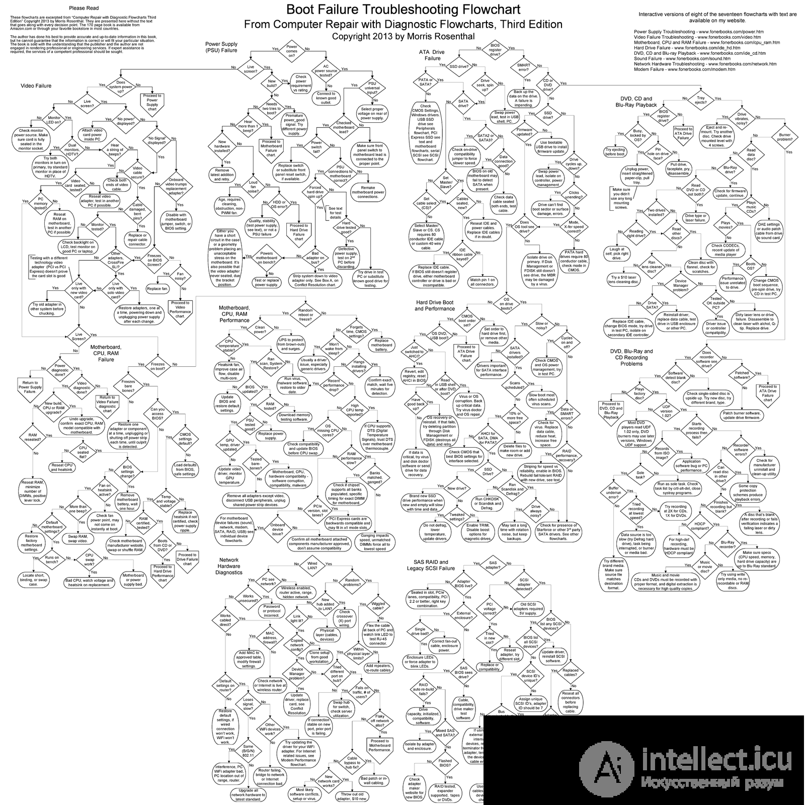
It should be understood that there is no ready-made solution for diagnosing and troubleshooting a laptop, since each model has its own peculiarities, however there are certain regularities arising from the fact that every laptop consists of typical parts. see fig. 1.
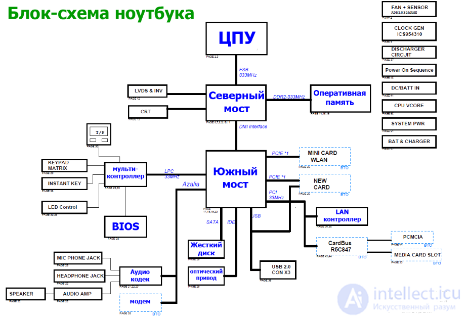
Most electrical schematics have, on their first pages, a block diagram that provides information about all the components of the board in summary form.
It contains a lot of information:
- CPU socket.
- PCH or northbridge
- southbridge.
- BIOS (you can also see, on the board, one or two BIOS chips are used).
- the name of the main components.
- in some schematics, there is also a block page information.
The main components of the motherboard:
One way or another, in different implementation variants (in one package or in different ones, on one board or on different ones)
these units are present in any laptop.
Provided these parts on the motherboard are functional and present, the laptop can start,
but for the laptop to work normally, the following are also required:
a hard drive, a matrix (display), a keyboard, and preferably a mouse or touchpad, a LAN controller.
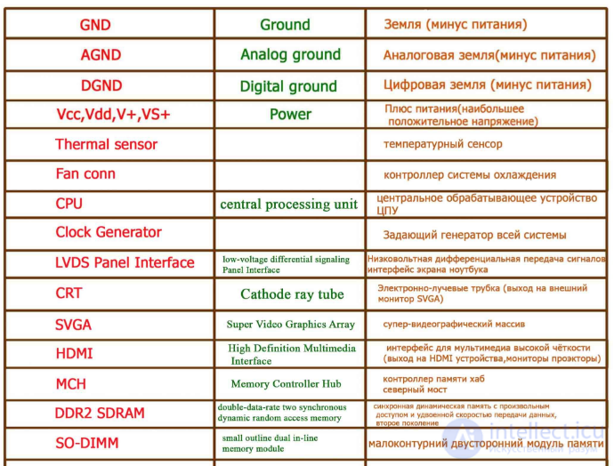
Signal names go far back into the past when there were transistors, also the origin of the signals is words from English
GND-ground,
CORE-core.
VCC, VEE, VDD, VSS
Power rail designations stem from the field of transistor circuit analysis, where a circuit with a transistor and resistors connected to it is usually considered. The voltage (relative to ground) at the collector, emitter, and base is denoted VC, VE, and VB.
The resistors connected to the transistor terminals are denoted RC, RE, and RB.
The voltage at the far (from the transistor) terminals of the resistors is often denoted VCC, VEE, and VBB. In practice, for example for an NPN transistor connected in a common-emitter configuration, VCC corresponds to the plus, and VEE to the minus of the power supply. Accordingly, for PNP transistors it will be the opposite.
Similar reasoning for N-type field-effect transistors and common-source circuits explains the designations VDD and VSS (D — drain; S — source): VDD — plus, VSS — minus. As written above, Vcc and Vee are used for circuits with bipolar transistors (VCC - plus, VEE — minus), and Vdd and Vss for circuits with field-effect transistors (VDD - plus, VSS — minus). This designation is not entirely correct, since chips consist of complementary pairs of transistors. For example, in CMOS chips, the plus is connected to the P-FET sources, and the minus to the N-FET sources. Nevertheless, this is the traditional established designation for power rails regardless of the conductivity type of the transistors used.
For circuits with dual-polarity power supply, VCC and VDD can be interpreted as the highest positive voltage, and VEE and VSS as the most negative voltage in the circuit relative to ground.
Ground can be of different types, for example, signal ground, chassis connection, earth ground.
Some designations:
The operation of all the laptop's units is ensured by the power subsystem.
This is a separate, quite complex part of the overall circuit in terms of organization. It is usually organized around a set of
so-called PWM controllers, providing the necessary power supply voltage level for the main and less critical chips.
If a computer regularly hangs or «doesn't like» a certain user, this does not indicate the latter's mystical abilities, but rather that they are generating excess static charge. The best way to get rid of this is to properly ground the power cord, as well as the network and modem cables.
Radio interference (radio frequency interference) can occur near powerful radio transmitters or cellular base stations. It manifests as nonspecific freezes, which are eliminated if the laptop is moved to another location. Shielded cables can help, which, incidentally, can be made by yourself – it is enough to put a ferrite ring core on the cable.
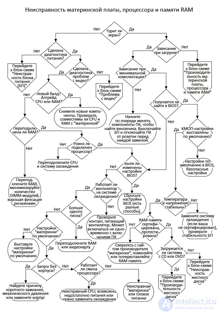
But there is a more unfortunate situation – Windows / Linux / MacOS does not boot. Let's try to fix it. At OS startup, hold F8 for a while, until the additional Windows / Linux / MacOS / BIOS boot options menu appears. You can move around using the arrow keys or the mouse, depending on the OS. Of the modes presented (if we are using Windows) we only need three:
1. Enable VGA mode – the operating system boots using the default settings for the graphics card. This mode helps when an incompatible video driver is installed, when a game does not replace the standard driver with one optimized for it and, after a freeze, does not perform the reverse replacement.
2. Loading the last known good configuration (in Windows Vista, to do this you first need to enter Safe Mode and select «System Restore») – the operating system boots using the registry data and drivers saved during the last successful shutdown. All changes made since the last boot will be lost. This option does not fix problems caused by damaged or missing drivers or files, but only allows the OS to be restored in case of problems caused by viruses or an incorrectly configured driver. If the graphical interface no longer loads, use the command line: C: \%systemroot%system32/restore/ rstrui.exe.
3. Safe Mode – the operating system boots using only the files necessary to start the main components of Windows, moreover with default settings. For example, a «universal» driver is used for the mouse, which will not support anything except the right/left button. If the boot fails – hold down the Esc key while this mode is loading, this will prevent non-Microsoft drivers from being loaded. If you managed to boot and the cause of the malfunction is known – fix it. If not – try to remember whether you installed any new programs or drivers in the previous session, or changed any settings. If the problem is with drivers and the new driver turned out to be worse than the old one – you need to revert everything back. Select the device in Device Manager, go to the Driver tab, click Roll Back and follow the instructions. If this does not help, keep searching for the problem.
The simplest option – check the system disk for errors (see the section «Maintaining laptop operability» for this), and check the files with an antivirus, preferably with updated signature databases and set to scan all files (scanning in safe mode is much more effective than in normal mode). Oddly enough, 96% of problems are solved exactly this way. But you'll have to work harder with the remaining 5%.
In the folder C: WindowsSystem there is a utility sfc.exe. It checks the integrity of system files and, if it finds damage, reinstalls them. This is an excellent tool when there are suspicions that the computer is infected (with a worm, trojan), and the antivirus is silent. However, most activation cracks, as well as manual editing of system files, lead to «unauthorized access» to files from sfc.exe's point of view. So you should keep a clear list of the files that sfc.exe has returned to a «normal» state.
So, if «cleaning» did not help, check the list of hardware in Device Manager , there should be no components with a question mark or exclamation mark. No, the computer can still work this way, but its stability and performance will be low. If for some reason it does not work, most likely these devices are not needed – disable them via BIOS, and if that does not work or you are afraid of doing something wrong, then do it via Device Manager (although this is not entirely correct and may not solve the problem, since the OS sees these «incorrect» devices, even though it does not use them).
Now let's move from software manipulations to hardware ones. If Windows cannot load its kernel (the files hal.dll or ntdll.dll), then most likely the problem is either a virus, or the RAM is malfunctioning. With constant freezes, it is worth cleaning the laptop of dust – let me remind you that dust is not only a good thermal insulator, but can also conduct electricity (small, of course, but quite sufficient for something to glitch due to induced interference). Enter the BIOS and reset the settings to the default ones (in the EXIT section there is usually a special item).
If nothing works – then you need to reinstall the OS. Only you need to make a backup copy of the drivers already in the system (all at once or individually). After all, some drivers are simply not publicly available.
Remember that it is better not to throw away a desktop PC, even if it is outdated. Computer hardware is mortal, like everything in this sublunary world, so an old PC will come in handy if, during a repair, you need to go online and search for information, download new drivers. And if something stops working, remember one of Murphy's laws more often: «If nothing works, finally read the instructions». Right after purchase, you should at least figure out the purpose of the additional buttons on the case. After all, there is nothing more annoying than discovering unused functionality a year or two later. If nothing helped – reinstall the OS, take it to a repair shop, or call a computer specialist to your home – the choice is yours.
Diagnosing a laptop fault is a complex topic and everyone has their own approach to solving this problem. In this article we want to share our experience of detecting motherboard faults. Of course, it is not possible to fully cover all the nuances and problems that arise when testing boards in a single article. Therefore, we will present the material in condensed form, so that the diagnostic principle is understandable.
There are many reasons for a laptop's inoperability. Therefore, let's consider the most difficult cases, in which standard operations, such as block replacement of components, do not help and everything comes down to the inoperability of the motherboard.
The problem, due to which the motherboard does not work, may be hidden at the stage before or after the execution of the BIOS instructions.
In this article we will look at problems that occur before BIOS execution.
As an example we will take the A6F laptop.
In order to figure out why the board shows no signs of life, we first need to understand the power distribution scheme and the startup sequence (Power On Sequence).
The startup sequence is a schematic representation of the board's startup process, from the moment voltages are applied to the board until the processor is ready to execute BIOS tasks.
The entire startup process is divided into 14 stages, at each of which you can see what is happening with the board, and if the board does not start, then by checking step by step 1-14, you can determine at which stage the problem occurred and eliminate it.
This is what the startup sequence of the A6F laptop looks like.
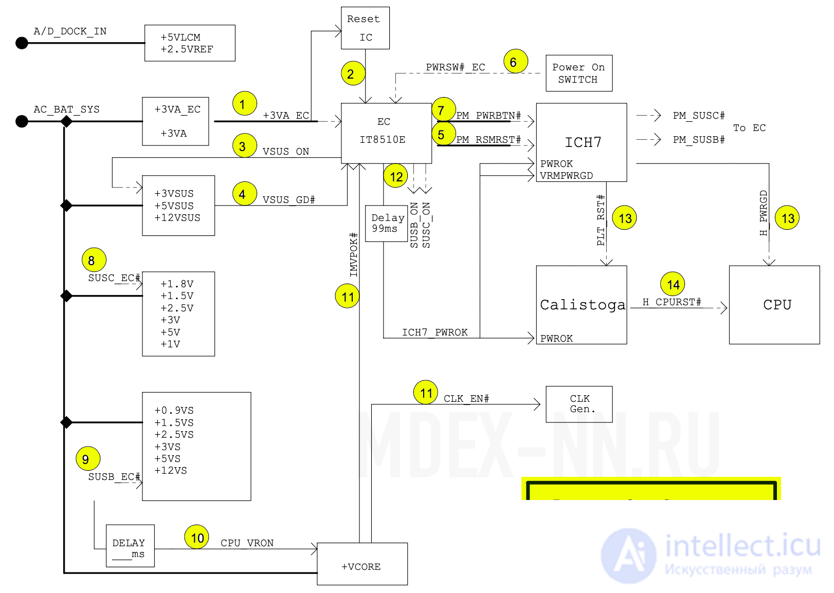
Let's go through the startup sequence step by step and look at the typical problems at each stage of startup.
As we can see, the entire process is divided into 14 stages, but before stage 1 is executed there is one more stage no less important for diagnostics. It is responsible for supplying input voltages to the board. Let's conditionally designate this stage as «0-1».
0-1 Input voltages (voltages from the AD_DOCK_IN and AC_BAT_SYS power sources)
Absence of input voltages is a common problem. This happens due to poor-quality power supplies or due to overload caused by high consumption of any of the components using external power.
The input voltage (19V) travels a distance with checkpoints and does not always reach the finish line. This distance can be represented in a simplified block diagram:

In more detail, the section of the circuit (Connector – Pmosfet) looks as follows:
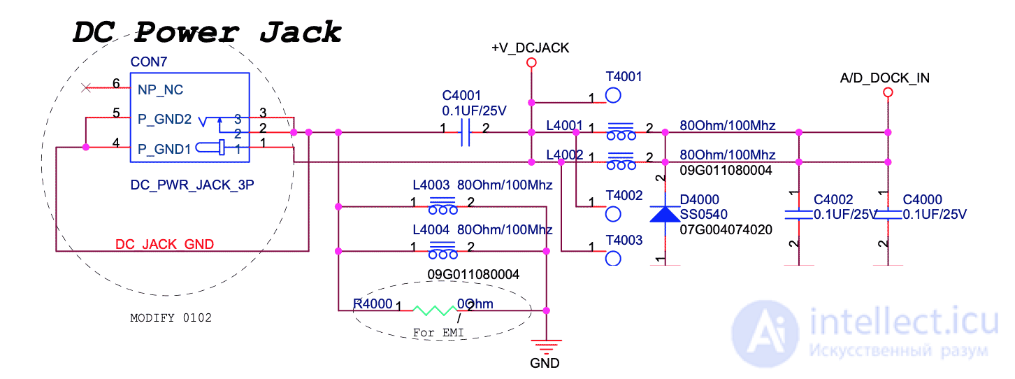
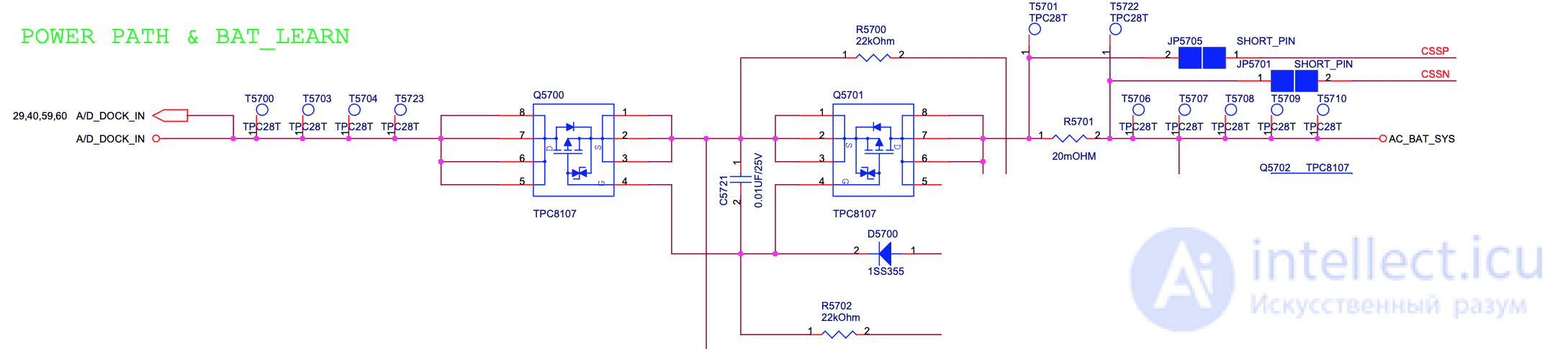
It is necessary to rule out a short circuit (SC) on AC_BAT_SYS (19V). Most often a short circuit ends no further than the power transistors in circuits requiring high power (processor power, video card) or on ceramic capacitors. Otherwise it is necessary to check everything that AC_BAT_SYS touches.
If there is no short circuit, we pay attention to the charge controller and the P-MOS transistors, which act as a kind of «swing bridge» between the power supply and the battery. The charge controller performs the function of switching the input voltages. To understand the operating process, let's refer to the datasheet, in which we are interested in the minimum operating conditions of the charge controller:
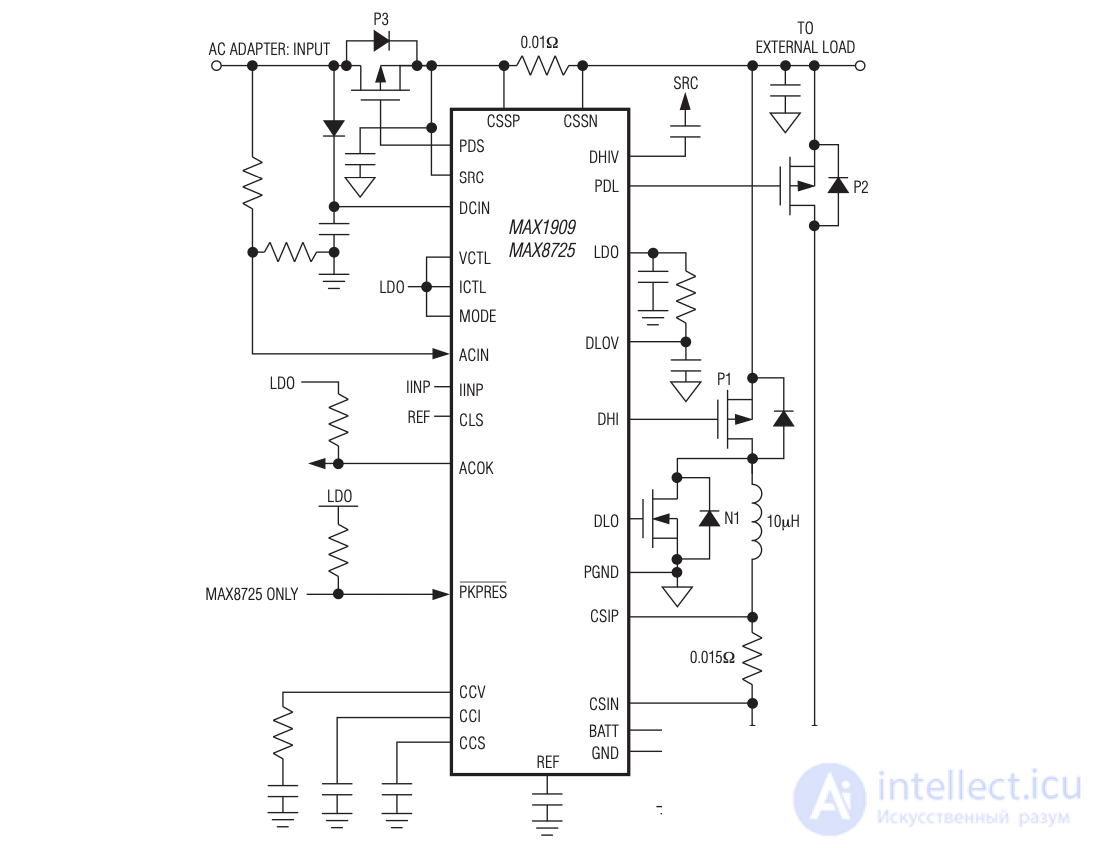
As can be seen from the diagram, the MAX8725 controller controls transistors P3 and P2. Thereby switching the PSU and battery power sources.
P3 is responsible for the power supply, P2 – for the battery. It is necessary to check the functionality of these transistors.
Let's look at the operating principle of the controller:
In the absence of main power, the controller automatically closes transistor P3 (control signal PDS), thereby blocking the power supply's access to the motherboard, and opens transistor P2 (control signal PDL). In this case the board can only operate from the battery. If we connect the power supply, the controller must cut off battery power by closing P2 and opening P3, providing power from the external power supply and charging the battery.
When diagnosing the input voltage from the mains, we do not use the battery and check only the PDS signal. In normal mode it should be pulled to ground, thereby opening the P-MOS and passing 19V to the board. If the controller does not properly control transistor P3, then it is necessary to check whether the controller itself is powered.
Then we check the main signals DCIN, ACIN, ACOK, PDS. If the signals are absent, then we replace the controller and, just in case, the P-mos transistors.
If during diagnostics no problems with input voltages were found, or they were eliminated, but the board still does not work, then we move on to the next stage.
1-2 EC controller power.
Embedded Controller – designed to control the mobile platform (the laptop motherboard), both at the level of turning it on and off, and for processing ACPI events. The tasks of the EC controller include servicing the battery: selecting its charging mode, monitoring discharge. As a rule, the keyboard controller is also implemented using the EC controller.
This chip is also often called SMC (System Management Controller) or MIO (Multi Input Output)
The chip is unique in that it has a large number of General Purpose Input/Output (GPIO) pins, which are programmed specifically for a particular platform. The program controlling this controller is most often stored together with the BIOS or on a separate FLASH chip.
Returning to diagnostics, let's look at the startup sequence, item 1. At this stage we are interested in the +3VA_EC voltage. It is the main power for the EC controller and the BIOS chip.
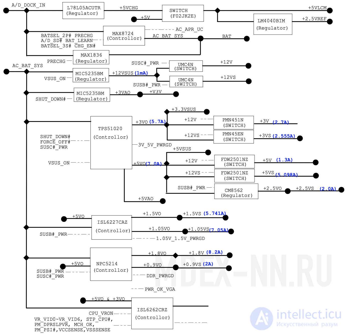
Judging by the power distribution scheme, this voltage is generated by the MIC5236YM linear regulator:
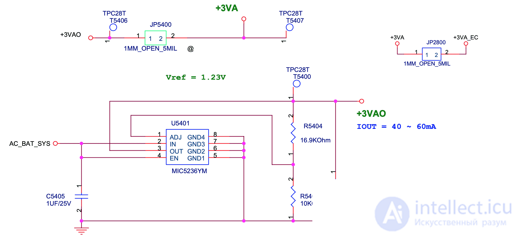
Thanks to the presence of the AC_BAT_SYS signal, which we discussed earlier, the chip must output the +3VAO voltage, which via diagnostic jumpers is converted into +3VA and +3VA_EC.
+3VA and +3VA_EC power the Embedded controller and BIOS, at which point the main board logic starts running, which is executed inside the EC controller. If these voltages are absent, then we figure out why.
Reasons for the absence of +3VA and +3VA_EC:
1) A short circuit inside components (EC, BIOS, etc.) that are powered from these voltages.
2) Damage to the linear regulator or its surrounding components.
Having dealt with +3VA and +3VA_EC, we move on to the next stage.
3 Standby voltages (+3VSUS, +5VSUS, +12VSUS).
After the EC has been powered and has read its firmware, the controller issues an enabling signal VSUS_ON to supply the standby voltages (see item 3 of the startup sequence). This signal goes to the switching power system headed by the TPS51020 chip:
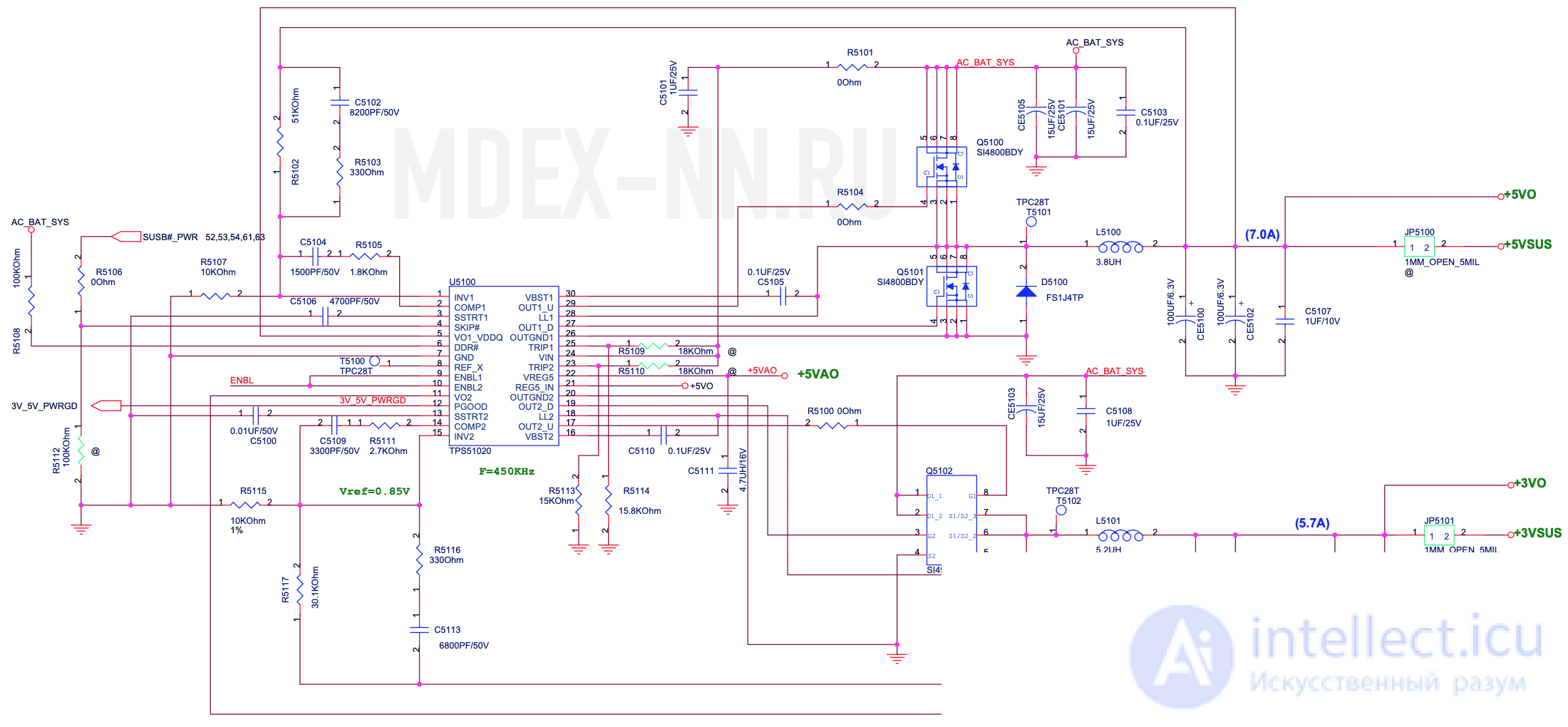
As can be seen in the diagram, we are interested in the voltages marked in green on the diagram: +5VO, +5VSUS, +3VO, +3VSUS.
In order for these voltages to appear on the board, the chip must be powered by 19V (AC_BAT_SYS) and enabling signals ENBL1 and ENBL2 must be present at pins 9, 10.

The enabling signals on the A6F platform are formed from the FORCE_OFF# and VSUS_ON signals.
First of all, attention should be paid to VSUS_ON, which is issued by the EC controller, and the FORCE_OFF# signal will be discussed later.
Absence of the VSUS_ON signal indicates that either the firmware (stored in the BIOS) is damaged, or the EC controller itself.
If the ENBL voltage is present on the board and TPS51020 is powered, then TPS51020 should generate +5VO, +5VSUS, +3VO, +3VSUS. We check them with a multimeter at the corresponding test points.
If the +5VO, +3VO voltages are not generated, we check these lines for a short circuit or reduced resistance.
If a short circuit is found, we break the circuit and determine which component is causing it.
If there is no short circuit, or after it has been eliminated, we check the voltages again, and if they are still absent, we replace the controller itself along with the transistors it controls.
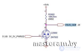
4 VSUS_GD# signal
At this stage the standby voltage controller informs the EC controller that the standby power is normal.
There should not be any problems, except that the intermediate transistor between the EC and TPS51020 has failed.
5 RSMRST# signal
RSMRST# – A resume and reset signal output. At this stage the EC controller issues a signal that the system is ready to power on. This signal passes directly between the EC and the south bridge. If it is absent, the cause could be the controller itself, the south bridge, or the EC firmware.
The simplest thing is to first reflash the BIOS, where the EC firmware is stored.
If there is no result, we desolder and lift pin 105 of the EC corresponding to the RSMRST# signal, and check the signal output at the EC controller. If the signal still does not come out, then we replace the controller.
If the signal comes out but does not reach the south bridge, then we check the south bridge and the real-time clock crystal; in the worst case the south bridge itself will need to be replaced.
6 Power button (PWRSW#_EC signal)
At this stage it is necessary to check the passage of the signal from the power button to the EC controller. To do this, we measure the voltage on the button and check its functionality; if after pressing the voltage does not drop, then the problem is in the button. It is also possible to short this signal to ground and check power-on.
7 Power-on signal (PM_PWRBTN# signal)
After the signal from the power button reaches the EC, the EC in turn passes this signal in the form of PM_PWRBTN# to the south bridge.
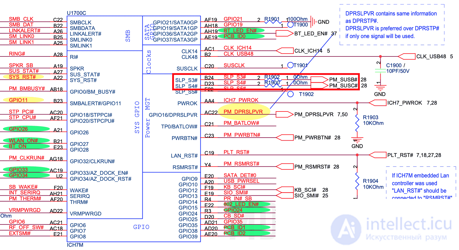
If the south bridge successfully receives it, then the next stage is issuing a response in the form of two signals PM_SUSC#, PM_SUSB#, which in turn are the south bridge's permission for the EC controller to turn on the main board voltages.
If the south bridge does not react to the PM_PWRBTN# signal in any way, then the problem lies within it.
8-9 Main voltages
As already mentioned earlier, the EC controller processes ACPI events.
But how exactly? In the previous item it was mentioned that the south bridge sends two signals to the EC: PM_SUSC#, PM_SUSB#. These signals are also called SLP_S3# and SLP_S4#; this is marked with a red block in the following diagram:
Let's take a closer look at the ACPI states:
A.C.P.I.
– S0–Working Status
– S1–POS(Power on Suspend)
– S3–STR(Suspend to RAM), Memory Working
– S4–STD(Suspend to Disk), H.D.D. Working
– S5–Soft Off
So, the state of these signals is responsible for the ACPI power state on the motherboard:
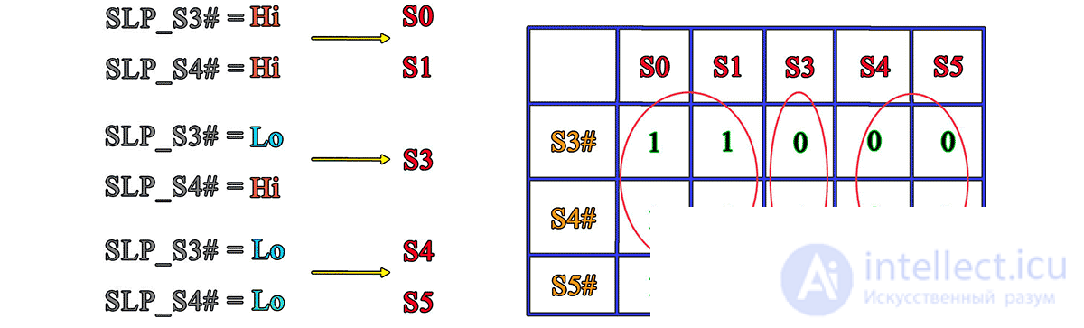
We will consider the case when both signals SLP_S3# and SLP_S4#, and accordingly the signals SUSC_EC#, SUSB_EC#, are in the HI state. That is, the motherboard is in S0 mode (fully working, all voltages present).
As can be seen from the startup sequence, when the SUSC_EC#, SUSB_EC# signals appear, the following voltages should appear on the board:
SUSC_EC# is responsible for the voltages: +1.8V, +1.5V, +2.5V, +3V, +5V, +1V;
SUSB_EC# is responsible for the voltages: +0.9VS, +1.5VS, +2.5VS, +3VS, +5VS, +12VS
If even one of these voltages is missing, the board will not start, so we check each power system, starting from +1.8V and ending with +12VS.
The SUSC_EC#, SUSB_EC# signals go both to the ENABLE inputs of individual switching power systems (for example, 1.8V DUAL – memory power supply), and to entire voltage cascades, converting previously existing standby voltages into the main ones:
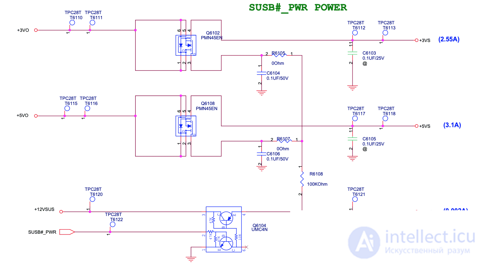
10 CPU power
We check the enable signal VRON, which, with a certain delay, arrives at the CPU power controller immediately after the SUSC_EC#, SUSB_EC# signals are issued. Next, voltage should appear on the CPU; if this did not happen, we investigate the power controller and its surrounding circuitry. There are quite a few reasons for the CPU power system to malfunction. The main one is failure of the controller itself. It is necessary to check the minimum operating conditions, for which the controller's datasheet and the schematic itself will be helpful.
11 Turning on the clock generator
After the CPU voltage appears on the board, the controller should issue 2 signals: IMVPOK# (Intel Mobile Voltage Positioning – OK) and CLK_EN#. The IMVPOK# signal notifies the EC that the CPU power is normal, and the CLK_EN# signal enables clock generation for the main logic units. To check the operability of the ICS954310 clocker, it is necessary to measure the frequency on at least one of the pins where the clock frequency is lowest, or one that your oscilloscope can catch. Let's choose pin 12 of the ICS954310 for this, which is responsible for outputting FSLA/USB_48MHz. If there is no generation, then we check the minimum operating conditions for the ICS954310. These are a 14MHz crystal and 3VS and 3VS_CLK power.
12 Final power-ready signal (PWROK).
If this signal is present, and the EC logic is functional, this means that all voltages on the board should be enabled.
13 PLT_RST#, H_PWRGD
PLT_RST# – the reset signal for the north bridge, H_PWRGD informs the processor that the north bridge power is normal.
If problems arise with these signals, we check the operability of the north and south bridges.
Checking bridges is a topic deserving a separate article. But in brief, it can be said that it is necessary to check the resistances along all power lines of these bridges, and if there is a deviation from the norm, the bridges need to be replaced. Also, a normal diode continuity check of the signal lines can identify a faulty bridge, but because these complex chips are soldered using BGA technology, it is practically impossible to reach the pins. These pins do not always come out to elements that are easy to reach with a tester probe. Therefore, there is a more convenient way to reach the pins – auxiliary diagnostic boards, which are inserted into connectors that go directly to the bridge pins. For example, a diagnostic board for checking the north bridge and memory channels.
14 Final stage of the startup sequence
H_CPURST# – reset signal issued by the north bridge to the CPU.
After the sequence completes, execution of the BIOS instructions begins.

Comments