
Lecture
Solid-state drive (SSD) is a non-mechanical, non-volatile computer storage device based on memory chips, serving as an alternative to the HDD. In addition to memory chips, an SSD contains a control controller. The most common type of solid-state drive uses NAND-type flash memory to store data, although variants exist in which the drive is built on DRAM memory equipped with an additional power source — a battery.
Solid-state drives are currently used both in portable devices (laptops, netbooks, tablets) and in desktop computers to boost performance. As of 2016, the highest-performing drives were M.2-format SSDs with an NVMe interface, which, with a suitable connection, could reach read/write speeds of up to 3800 megabytes per second.
Compared to traditional hard disk drives (HDDs), solid-state drives are smaller and lighter, are silent, and are many times more resistant to damage (for example, from being dropped), and offer much higher speeds for random operations. At the same time, they cost several times more per gigabyte and have lower durability (write endurance).
Flash memory is a type of semiconductor technology based on electrically reprogrammable memory (EEPROM). The same term is used in electronic circuit design to refer to technologically finished solutions for read-only memory devices in the form of chips based on this semiconductor technology. In everyday usage, the term has come to be applied to a broad class of solid-state data storage devices.
Thanks to its compactness, low cost, mechanical durability, large capacity, speed, and low power consumption, flash memory is widely used in digital portable devices and storage media. A serious drawback of this technology is the limited endurance of the media, as well as sensitivity to electrostatic discharge.
The predecessors of flash memory technology can be considered to be ultraviolet-erasable programmable read-only memory (EPROM) and electrically erasable programmable read-only memory (EEPROM). These devices also had an array of floating-gate transistors, in which electron injection into the floating gate ("writing") was achieved by creating a high electric field strength in a thin dielectric. However, the layout area of the components in the array increased sharply if a reverse-polarity field was required to remove electrons from the floating gate ("erasing"). This is why two classes of devices emerged: in one case, erase circuitry was sacrificed to obtain high-density, write-once memory, while in the other case, a fully functional device with much lower capacity was made.
Accordingly, engineers focused their efforts on solving the problem of packing density for erase circuits. Their efforts were successful — the invention by Toshiba engineer Fujio Masuoka (舛岡富士雄) in 1984. The name "flash" was also coined at Toshiba — by Shoji Ariizumi, to whom the process of erasing memory contents reminded him of a photographic flash. Masuoka presented his development in 1984 at the IEEE International Electron Devices Meeting (IEDM), held in San Francisco.
In 1988, Intel released the first commercial NOR-type flash chip.
NAND-type flash memory was announced by Toshiba in 1989 at the International Solid-State Circuits Conference.
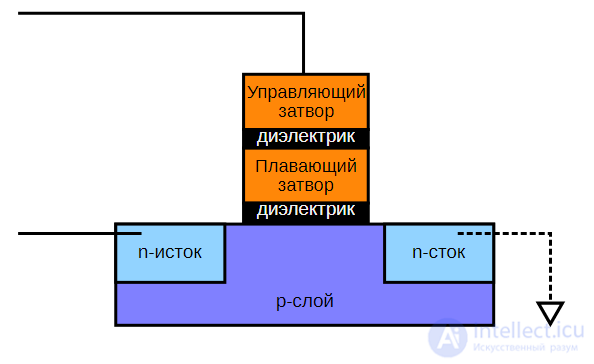
The main component in flash memory is the floating-gate transistor, a type of MOSFET. Its distinguishing feature is that it has an additional gate (floating), located between the control gate and the p-layer. The floating gate is isolated, and the negative charge stored in it will remain there for a long time.
A distinction is made between devices in which the elementary cell stores one bit of information and those that store several bits. In single-bit cells, only two charge levels are distinguished on the floating gate. Such cells are called single-level cells (SLC). In multi-bit cells, more charge levels are distinguished; these are called multi-level cells (MLC). MLC devices are cheaper and have higher capacity than SLC devices, but have longer access times and roughly an order of magnitude fewer maximum rewrite cycles.
MLC usually refers to memory with 4 charge levels (2 bits) per cell. Memory that is cheaper per unit of capacity, with 8 levels (3 bits), is called TLC (Triple Level Cell) or 3-bit MLC (as Samsung calls it). There are also devices with 16 levels per cell (4 bits), QLC (quad-level cell). In August 2018, Samsung Electronics announced the start of mass production of SSDs using QLC V-NAND memory.
By 2016, multi-level memory dominated the market. Nevertheless, SLC products, despite their much lower capacity, continue to be developed and manufactured for particularly critical applications.
A natural extension of the MLC cell concept was the idea of storing an analog signal in a cell. Such analog flash chips found their greatest application in playing back relatively short audio clips in cheap, mass-produced products. Such chips can be used in simple toys, sound greeting cards, answering machines, and so on.
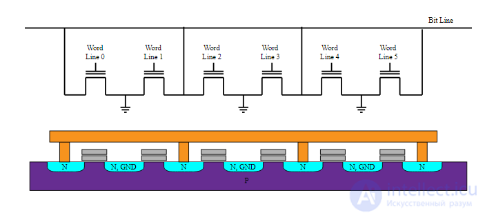
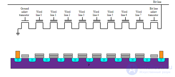
Flash memory types differ in the method used to connect cells into an array.
The NOR design uses a classic two-dimensional matrix of conductors, with one cell placed at each intersection of rows and columns. Here, the row conductor was connected to the transistor's drain, and the column conductor to the second gate. The source was connected to a common substrate shared by all cells.
The NAND design is a three-dimensional array. It is based on the same matrix as NOR, but instead of a single transistor at each intersection, a column of series-connected cells is placed. This design results in many gate circuits at a single intersection. The packing density can be sharply increased (since only one gate conductor reaches each cell in a column), but the algorithm for accessing cells for reading and writing becomes noticeably more complex. Also, two MOSFETs are installed on each line: a bit line select transistor, located between the column of cells and the bit line, and a ground select transistor, located before the ground.
NOR technology allows fast access to each individual cell, but the cell area is large. NAND, on the other hand, has a small cell area but relatively long access times to a large group of cells at once. Accordingly, their application areas differ: NOR is used as direct program memory for microprocessors and for storing small amounts of auxiliary data.
The names NOR and NAND arose by association between the circuit used to connect cells into an array and the circuit design of CMOS logic — NOR and NAND gates.
NAND is most often used for USB flash drives, memory cards, and SSDs, while NOR is used in embedded systems.
Other ways of combining cells into an array existed but did not become widespread.
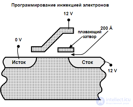
Fig. Programming flash memory
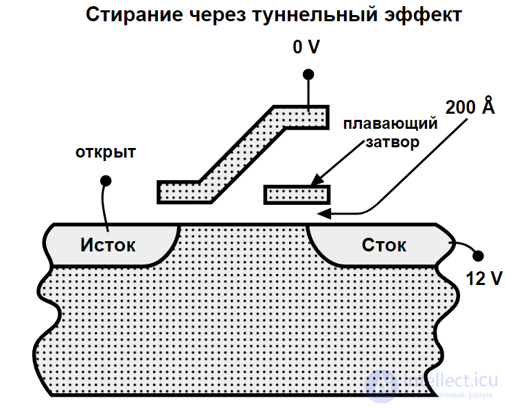
Fig. Erasing flash memory
To read, a positive voltage is applied to the control gate. If there is no charge in the floating gate, the transistor will begin conducting current. Otherwise, no current arises between the source and drain. For MLC cells, several measurements must be taken.
To read a specific memory cell, an intermediate voltage must be applied to its control gate (sufficient for the transistor to conduct only if there is no charge in the floating gate). The remaining cells on the line must be given a minimum voltage to prevent them from conducting. If the cell of interest has no charge, current will flow between the bit line and ground.
In this arrangement, an intermediate voltage is likewise applied to the control gate of a specific cell. The remaining control gates on the line are given an elevated voltage to ensure they conduct current. Thus, current will flow between ground and the line if the cell of interest has no charge.
To write, charges must reach the floating gate, but it is isolated by an oxide layer. The tunneling effect can be used to transfer charges. To erase a charge, a large positive voltage must be applied to the control gate: the negative charge will leave the floating gate via the tunneling effect. Conversely, to charge the floating gate, a large negative voltage must be applied.
Writing can also be implemented using hot-carrier injection. When current flows between the source and drain at an elevated voltage, electrons can overcome the oxide layer and remain in the floating gate. This requires a positive charge to be present on the control gate, which creates the potential needed for injection.
In MLC, different voltages and application times are used to write different values.
Each write operation causes minor damage to the oxide layer, so the number of writes is limited, which directly affects the reliability of an SSD.
Writing in NOR and NAND layouts consists of two stages: first, all transistors on the line are set to 1 (no charge), then the required cells are set to 0.
In the first stage, cells are cleared using the tunneling effect: a strong voltage is applied to all control gates. To set a specific cell to 0, hot-carrier injection is used. A large voltage is applied to the bit line. A second important condition for this effect is the presence of positive charges on the control gate. Positive voltage is applied only to certain transistors; negative voltage is applied to the rest. In this way, zero is written only into the cells of interest.
The first stage in NAND is similar to NOR. To set a zero in a cell, the tunneling effect is used, unlike in NOR. A large negative voltage is applied to the control gates of interest.

NAND circuit design turned out to be convenient for building a vertical arrangement of a cell block on a chip. Conducting and insulating layers are deposited layer by layer on the chip, forming the gate conductors and the gates themselves. Then, a large number of holes are formed through the full depth of these layers. The structure of field-effect transistors — insulators and floating gates — is applied to the walls of the holes. In this way, a column of ring-shaped field-effect transistors with floating gates is formed.
This vertical structure proved very successful and provided a qualitative leap in flash memory density. Some companies market this technology under their own trademarks, such as V-NAND and BiCS. The number of layers has increased as the technology developed: by 2016, the number of layers in some products reached 64, in 2018 production of 96-layer memory was mastered, and in 2019 Samsung announced mass production of 136-layer chips.
To save space, a single flash memory chip may package several semiconductor wafers (dies), up to 16 of them.
Writing and reading cells differ in power consumption: flash memory devices draw a large current during writing to generate high voltages, whereas the energy cost of reading is relatively small.
Erasing, writing, and reading flash memory always occurs in relatively large blocks of varying sizes, with the erase block size always larger than the write block size, and the write block size never smaller than the read block size. This is, in fact, the characteristic feature that distinguishes flash memory from classic EEPROM memory.
As a consequence, all flash memory chips have a clearly defined hierarchical structure. Memory is divided into blocks, blocks consist of sectors, and sectors consist of pages. The depth of this hierarchy and the size of its elements can vary depending on the intended purpose of a particular chip.
For example, a NAND chip may have an erase block size of hundreds of kilobytes, with a write/read page size of 4 kilobytes. For NOR chips, the erase block size ranges from units to hundreds of kilobytes, the write sector size is up to hundreds of bytes, and the read page size is units to tens of bytes.
Erase speed varies from units to hundreds of milliseconds depending on the size of the block being erased. Write speed is tens to hundreds of microseconds.
Typically, read speed for NOR chips is rated in tens of nanoseconds. For NAND chips, read speed is tens of microseconds.
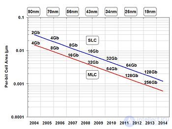
Because of its highly regular structure and high demand for large capacities, the manufacturing process for NAND flash memory shrinks more quickly than for the less regular DRAM memory and the nearly irregular logic (ASIC). Intense competition among several leading manufacturers only accelerates this process[24]. Under the variant of Moore's law applicable to logic chips, the number of transistors per unit area doubles every three years, whereas NAND flash has shown a doubling every two years. In 2012, a 19 nm process was mastered by the joint venture of Toshiba and SanDisk[25]. In November 2012[26], Samsung also began production using a 19 nm process (actively using the marketing phrase "10nm-class" to denote some process in the 10-19 nm range)[27][28][29][30].
| ITRS or company | 2010 | 2011 | 2012 | 2013 | 2014 | 2015* | 2016* |
|---|---|---|---|---|---|---|---|
| ITRS Flash Roadmap 2011[25] | 32 nm | 22 nm | 20 nm | 18 nm | 16 nm | ||
| ITRS Flash Roadmap 2013[31][32] | 17 nm | 15 nm | 14 nm | ||||
| Samsung[25][32] Samsung 3D NAND (CTF)[32] |
35-32 nm | 27 nm | 21 nm (MLC, TLC) | 19 nm | 19-16 nm V-NAND (24L) |
12 nm V-NAND (32L) |
12 nm |
| Micron, Intel[25][32] | 34-25 nm | 25 nm | 20 nm (MLC + HKMG) | 20 nm (TLC) | 16 nm | 12 nm 3D-NAND |
3D-NAND Gen2 |
| Toshiba, Sandisk[25][32] | 43-32 nm | 24 nm | 19 nm (MLC, TLC) | A-19 nm | 15 nm | 3D NAND BiCS | 3D NAND BiCS |
| SK Hynix[25][32] | 46-35 nm | 26 nm | 20 nm (MLC) | 20 nm | 16 nm | 3D V1 | 12 nm |
Shrinking the manufacturing process made it possible to rapidly increase the capacity of NAND flash memory chips. In 2000, flash memory using a 180 nm process had a data capacity of 512 Mbit per die; by 2005, this was 2 Gbit at 90 nm. There was then a transition to MLC, and by 2008 chips had a capacity of 8 Gbit (65 nm)[33]. In 2010, about 25-35% of chips had a capacity of 16 Gbit, and 55% had 32 Gbit[34]. In 2012-2014, dies with a capacity of 64 Gbit were widely used in new products, and the introduction of 128-Gbit modules began (10% at the start of 2014), manufactured using 24-19 nm processes[33][34].
As the manufacturing process shrinks and approaches the physical limits of current fabrication technologies, particularly photolithography, further increases in data density may be achieved by moving to a greater number of bits per cell (for example, transitioning from 2-bit MLC to 3-bit TLC), by replacing FG cell technology with CTF technology, or by transitioning to a three-dimensional cell arrangement on the wafer (3D NAND, V-NAND; although this increases the process step size). For example, around 2011-2012, all manufacturers introduced air gaps between control lines, which allowed scaling to continue beyond 24-26 nm[35][36], and starting in 2013-2014 Samsung began mass production of 24- and 32-layer 3D NAND[37] based on CTF technology, including in a variant with 3-bit (TLC) cells[39]. The decrease in endurance (erase cycle life) that appears as the process shrinks, along with an increase in the bit error rate, has required the use of more sophisticated error-correction mechanisms and reductions in guaranteed write volumes and warranty periods. However, despite the measures taken, it is likely that further scaling of NAND memory will become economically unjustifiable or physically impossible. Many possible replacements for flash memory technology are being researched, including FeRAM, MRAM, PMC, PCM, ReRAM, and so on.
The drive to reach the maximum possible capacity for NAND devices has led to the "standardization of defects" — the right to manufacture and sell chips with a certain percentage of defective cells and without any guarantee against new "bad blocks" appearing during operation. To minimize data loss, each memory page is equipped with a small additional block in which a checksum is recorded, along with information for recovering from single-bit errors, information about faulty elements on that page, and the number of writes to that page.
The complexity of the read algorithms and the acceptability of having a certain number of defective cells have forced developers to equip NAND memory chips with a specific command interface. This means that a special command must first be issued to transfer the specified memory page into a special buffer inside the chip, then the completion of this operation must be awaited, the buffer read out, the data integrity checked, and, if necessary, an attempt made to recover it.
A weak point of flash memory is the number of rewrite cycles per page. The situation is made worse by the fact that standard file systems — that is, standard file management systems for widely used file systems — often write data to the same location repeatedly. The file system's root directory is often updated, so the first sectors of memory will use up their allotted cycles much sooner. Load balancing (wear leveling) can substantially extend the memory's service life.
To simplify the use of NAND-type flash memory chips, they are used together with special chips — NAND controllers. These controllers must handle all the routine work of managing NAND memory: interface and protocol conversion, address virtualization (to bypass faulty cells), data verification and recovery during reads, handling the different sizes of erase and write blocks (write amplification), managing periodic refreshing of stored blocks, and evenly distributing the load across sectors during writing (wear leveling).
However, evenly distributing wear is not mandatory, so the cheapest products may, for the sake of cost savings, be equipped with the simplest controllers. Such flash memory cards and USB drives will quickly fail under frequent rewriting. When very frequent data writes to flash drives are required, it is preferable to use more expensive products with more durable memory (MLC instead of TLC, SLC instead of MLC) and high-quality controllers.
Expensive NAND controllers may also be tasked with "accelerating" flash memory chips by distributing the data of a single file across several chips. This significantly reduces file write and read times.
In embedded applications, flash memory is often connected directly to the device — without a controller. In this case, the controller's tasks must be performed by a software NAND driver within the operating system. To avoid doing redundant work to evenly distribute writes across pages, such media are typically used with special file systems: JFFS2 and YAFFS for Linux, among others.
There are two main ways flash memory is used: as a portable storage medium and as storage for the software ("firmware") of digital devices. These two applications are often combined in a single device.
Storing firmware in flash memory allows easy firmware updates for devices during operation.
NOR flash is best suited for devices with relatively small-capacity non-volatile memory that require fast access at random addresses and a guarantee of no faulty elements:
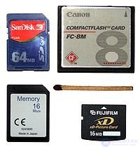
Where record-breaking storage capacities are required, NAND flash has no competition. NAND chips have shown steady growth in capacity, and by 2012 NAND held the record for an 8-die package with a capacity of 128 gigabytes (i.e., each die had a capacity of 16 gigabytes, or 128 gigabits)[49].
NAND flash memory is used primarily in all kinds of portable data storage media and devices that require large storage capacity for operation. These are mainly USB flash drives and memory cards of all types, as well as mobile devices such as phones, cameras, and media players.
NAND-type flash memory has made it possible to miniaturize and reduce the cost of computing platforms based on standard operating systems with advanced software. These have come to be embedded in a wide range of consumer devices: cell phones and televisions, network routers and access points, media players and game consoles, digital photo frames and navigation devices.
The high read speed makes NAND memory attractive for caching hard drives. Here, the operating system stores frequently used data on a relatively small solid-state device, while general-purpose data is written to a large-capacity disk drive[50]. It is also possible to combine a 4-8 GB flash buffer with a magnetic disk in a single device — a solid-state hybrid drive (SSHD).
Thanks to its high speed, capacity, and compact size, NAND memory is actively displacing other types of storage media. Floppy disks and floppy drives disappeared first[51], and the popularity of magnetic tape drives declined. Magnetic media have been almost entirely displaced from mobile and media applications.
Low-level interfaces
Standardization of packages, interfaces, command sets, and chip identification for NAND-type flash memory chips is handled by the Open NAND Flash Interface (ONFI) organization. The first standard was the ONFI version 1.0 specification[52], released on December 28, 2006, followed by ONFI V2.0, V2.1, V2.2, V2.3, and V3.0 (2011)[53]. The ONFI group is supported by Intel, Micron Technology, Hynix, and Numonyx.[54]
Samsung and Toshiba are developing their own alternative to ONFI, the Toggle Mode DDR standard. The first revision was released in 2009, the second in 2010.[53]
High-level interfaces
In addition to the standardization of the memory chips themselves, there is specific formalization of access to long-term memory from common digital interfaces. For example, the Non-Volatile Memory Host Controller Interface group handles the standardization of solid-state drive design for the PCI Express interface.
Standing apart are integrated memory-and-controller solutions in the form of chips — for example, embedded eMMC memory, which is widely used and employs an electrical interface similar to MMC but implemented as a single chip.[55] Development of this interface is handled by JEDEC.
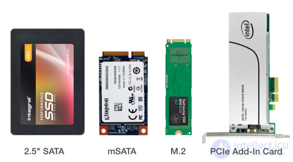
As I already mentioned at the beginning of the article, the market currently offers a huge number of different solid-state drives. The first thing that catches the eye is the variety of form factors. When choosing an SSD for your system, you may come across the following formats:
The SSD's connection interface directly affects its speed. More on this in the next section.
The maximum data transfer speed of a solid-state drive is limited by the type of connection.
Consumer-segment SSDs use connections via the SATA and PCI-Express interfaces:
Next, I would like to make a small digression and dwell in more detail on the M.2 standard and the NVMe protocol mentioned above.
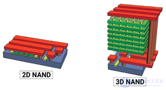
NAND flash is the main and most expensive component of a solid-state drive. Let's highlight three main types of memory used in modern SSDs:
Since 3D NAND is the most common type of memory in solid-state drives, let's take a closer look at its types and operating principle.
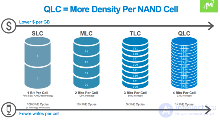
Density difference between types of 3D NAND memory. Source: Micron
The type of 3D NAND memory used in a drive directly affects its efficiency and durability. Currently, you can encounter the following types of 3D NAND memory in solid-state drives:
The most important difference between the various types of 3D NAND memory is their durability. To understand what causes this difference, let's look at the operating principle of 3D NAND memory.
NAND memory consists of floating-gate transistor cells that retain a charged state in the absence of a power source. Floating gates contain electrons, and the charged state is represented by the binary digit 0, while the discharged state is represented by 1. The binary bit 0 represents data stored in NAND memory.
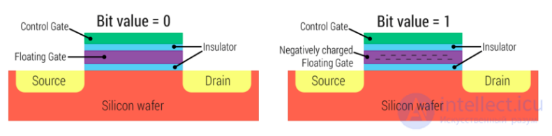
Operating principle of NAND memory
Cells are arranged in a grid known as a block. A single row within a block is called a page and supports sizes of 2K, 4K, 8K, and 16K. Each block contains 128-256 pages, so its approximate size ranges from 256KB to 4MB.
3D NAND memory of the SLC type stores 1 bit of information, MLC stores 2 bits, and TLC stores 3 bits. This arrangement looks as follows.
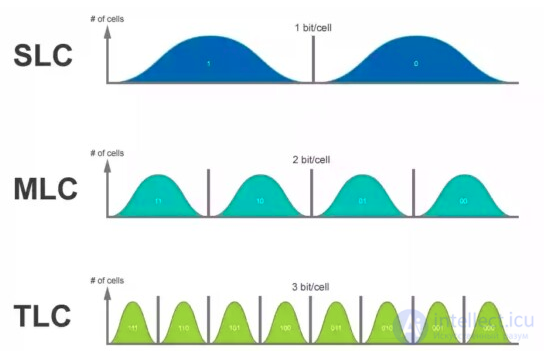
Density of the most common types of 3D NAND memory
Flash memory stores information by trapping electrons in cells. The charge assigned to a cell determines the presence of data. The process of electrons entering and exiting has a negative effect on the cell's structure, and some electrons get "stuck." These electrons create a negative charge, reducing the voltage range available for representing data. The smaller this range becomes, the harder it is for solid-state drives to perform writes and verify their accuracy.
The accumulation of electrons is particularly destructive at higher bit densities. MLC memory has to distinguish between four possible values within a shrinking voltage window, but TLC memory has to track twice as many values, and QLC four times as many. As a result, memory with a denser layout "burns out" faster, thereby having a shorter lifespan.
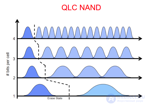
Continuing the write cycle eventually causes cells to become unreliable. These cells are subsequently removed and replaced with flash memory drawn from the drive's "spare area." This reserve of new flash memory area ensures that the solid-state drive retains its user-available storage capacity, even if the failure of individual cells takes part of the memory out of service. Eventually this reserve is also depleted, and the drive begins to fail.
When examining memory types in more detail, one cannot fail to mention a relatively recent development by Intel Corporation — 3D XPoint memory and Intel Optane drives based on it.
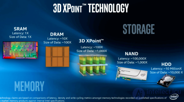
Intel and Micron began joint work on 3D XPoint memory in 2012. Previously, Intel and Micron had already collaborated on developing other types of non-volatile memory. The 3D XPoint architecture uses chalcogenide materials both for the selector and for storing data in memory cells. The technology is not based on electrons and uses changes in the electrical resistance of materials.
Unlike NAND memory, 3D XPoint has no binding of write operations to pages or erase operations to blocks. Furthermore, there is no need to delete data before a write operation. This allows for ultra-low latency and high read-write performance. And since operations with electrons are not used in 3D XPoint memory, its endurance is also very high.
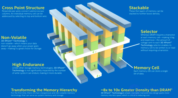
Structural layout of 3D XPoint memory. Source: Intel
Individual memory cells in XPoint are addressed using a selector, and no transistor is required to access them (unlike in NAND technology), which allows reducing the cell area and increasing their placement density on the die.
Intel releases devices based on 3D XPoint memory under the Optane brand, while Micron does so under the QuantX brand.
Consumer Intel Optane drives are divided into 3 main product lines:
If you compare the price per 1GB of 3D NAND memory and 1GB of 3D XPoint memory (based on drive prices), the latter is 3-4 times more expensive. However, the price difference is offset by high endurance and incredibly low access latency.
It's also worth noting that not all processors and chipsets support Intel Optane technology. To use this type of solid-state drive, you'll need an 8th generation processor or newer, and a motherboard with a 200 series chipset or newer.
With that, we can conclude this long digression on memory operating principles and return to explaining how individual components work. Next up is the memory controller.
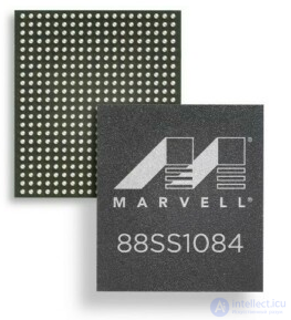
Every SSD includes a controller that connects the NAND memory components to your system. The controller is an embedded processor that executes firmware code and is one of the most important elements for the performance of a solid-state drive.
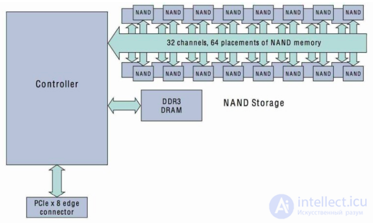
Diagram of memory controller operation
Let's look at some of the functions the memory controller is responsible for:
Controllers are created both by memory and solid-state drive manufacturers (Intel, Samsung, Toshiba, etc.) and by third-party companies (Marvell, SandForce, SiliconMotion, Phison). The controllers themselves, like the SSDs they are installed in, are divided into categories depending on the device's purpose. The most expensive and advanced models are installed in enterprise-segment drives, while basic ones go into budget consumer solutions.
The main consumer characteristics of an SSD that directly define its speed and operating efficiency are:
When listing the specifications of solid-state drives, you may come across mentions of support for TRIM and NCQ functions. Briefly, they work as follows:
SSD flash memory is built from blocks, which in turn consist of pages. Data is written to individual pages within blocks, and it is impossible to update data by simply overwriting the old data. Moreover, only an entire block can be erased at once!
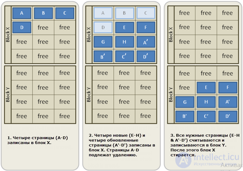
Therefore, the needed data is first moved from the pages of one block to another, and only then is the entire block erased along with the remaining unneeded data, thereby freeing it up for new writes. This process is called garbage collection.
TRIM is an operating system capability that marks unneeded data in a special way. This means the controller doesn't need to move it by writing it to other blocks. This increases write speed and, most importantly, significantly reduces the number of rewrite cycles.
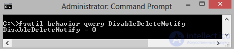
In modern versions of Windows this function is enabled (verified with the command above), but that doesn't necessarily mean it's actually working.
A solid-state drive's endurance directly depends on the number of rewrite cycles for its memory blocks. If data is regularly written to the same block, it will die quickly, thereby reducing the disk's capacity. Therefore, the controller's job is to evenly distribute data across all the SSD's blocks.
Obviously, garbage collection and wear leveling lead to an increase in the actual amount of data written to a solid-state drive (write amplification). Unlike with an HDD, this amount is much greater than what the programs and the system dictate.
There is no fixed multiplier, since the increase in volume depends on a number of factors, including the type of data being written.
Sequential writing (for example, copying files) does not lead to a significant increase in volume, since it's possible to fill blocks evenly. Random writing (for example, OS operation) involves much more active movement of data between the blocks of the solid-state drive.
Either way, the controller is tasked with efficiently distributing data across the disk, ensuring the maximum service life for all memory blocks.
Right now my main system drive is a Kingston Hyper-X 3K. "Hyper-X" is just a marketing name for the lineup, but "3K" reveals one of the drive's main technical characteristics — its endurance in terms of the amount of data written.
3K, or 3,000, is the number of rewrite cycles that the Intel 25nm MLC NAND flash memory underlying this drive can withstand. The Kingston Hyper-X model without the "3K" suffix is also based on 25nm memory, but withstands 5,000 cycles.
Let's calculate this using the example of a hypothetical 120GB drive that has 12GB written to it per day (this is quite a lot, as you'll see below). Let's assume that, under your workload, the controller increases the write volume by a factor of 10, which is also taken with a large margin.
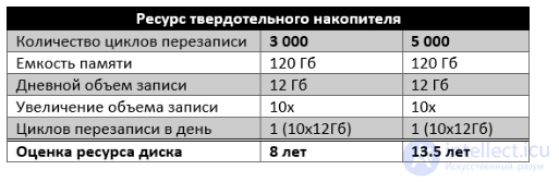
Under this scenario, you go through one rewrite cycle per day. Dividing the number of cycles by 365, we get 8.219 years for 3,000 cycles, and 13.698 years for 5,000 cycles (rounded values in the table). After that, theoretically, your data should remain intact for another 12 months, but it's possible this would only be true for reading.
Changing the charge is accompanied by the accumulation of irreversible changes in the structure, and therefore the number of writes for a flash memory cell is limited. Typical numbers of erase-write cycles range from tens or hundreds of thousands down to a thousand or less, depending on the type of memory and the manufacturing process. The guaranteed endurance is significantly lower when storing several bits per cell (MLC and TLC) and when using process nodes in the "30nm" class and more modern ones.
One reason for degradation is the impossibility of individually controlling the floating-gate charge in each cell. The fact is that writing and erasing are performed on many cells simultaneously — this is an inherent property of flash memory technology. The write circuitry monitors the sufficiency of charge injection based on a reference cell or an average value. Gradually, the charge of individual cells becomes misaligned, and at some point goes beyond the acceptable limits that the write circuitry can compensate for through injection and that the read device can interpret correctly. It's clear that the degree of cell uniformity affects endurance. One consequence of this is that as semiconductor technology's feature sizes shrink, it becomes increasingly difficult to create identical elements, so the issue of write endurance becomes more and more acute.
Another reason is the mutual diffusion of atoms between the insulating and conducting regions of the semiconductor structure, accelerated by the electric field gradient in the well region and periodic electrical breakdowns of the insulator during writing and erasing. This leads to blurring of boundaries and degradation of the insulator's quality, reducing charge retention time.
Initially, in the 2000s, for 56nm memory, this erase endurance was up to 10 thousand cycles for MLC devices and up to 100 thousand cycles for SLC devices, but as process nodes shrank, the guaranteed number of erase cycles decreased. For 34nm memory (early 2010s), regular 2-bit MLC guaranteed on the order of 3,000-5,000 cycles, and SLC up to 50,000. In 2013, some models guaranteed on the order of a few thousand cycles for MLC and less than a thousand (a few hundred) for TLC before the onset of degradation
| Memory Type | Endurance | Example Products |
|---|---|---|
| SLC NOR | 100,000 .. 1,000,000 | Numonyx M58BW, Spansion S29CD016J |
| MLC NOR | 100,000 | Numonyx J3 flash |
| SLC NAND | 100,000 | Samsung OneNAND KFW4G16Q2M |
| MLC NAND | 1000 .. 10,000 | Samsung K9G8G08U0M |
| TLC NAND | 1000 | Samsung SSD 840 |
| 3D MLC NAND | 6000 .. 40,000 | Samsung SSD 850 PRO, Samsung SSD 845DC PRO |
| 3D TLC NAND | 1000 .. 3000 | Samsung SSD 850 EVO, Samsung SSD 845DC EVO, Crucial MX300 |
Research is underway on an experimental technology for restoring flash memory cells by locally heating the gate insulator to 800°C for a few milliseconds.
The well's insulation is not ideal, and the charge gradually changes. The charge retention period claimed by most manufacturers for consumer products does not exceed 10-20 years, although the warranty on the media is given for no more than 5 years. At the same time, MLC memory has shorter retention periods than SLC.
Specific external conditions, such as elevated temperatures or radiation exposure (gamma radiation and high-energy particles), can catastrophically shorten the data retention period.
In modern NAND chips, reading can cause data corruption on neighboring pages within a block. Performing a large number (hundreds of thousands or more) of read operations without rewriting can accelerate the occurrence of errors.
Let's run a check on whether drives that have used up their manufacturer-rated endurance can reliably retain data while powered off.
Two weeks in a powered-off state had absolutely no effect whatsoever on the integrity of the information recorded on the SSDs. All of the tested drives were able to read both the information written immediately before being powered off and the files that had been stored on them since the very beginning of our endurance test. No failures or checksum discrepancies were recorded.
According to Dell, how long data is retained on SSDs disconnected from power depends heavily on the number of program/erase (P/E) cycles completed and on the type of flash memory, and in the worst cases it may be as short as 3-6 months
However, we still cannot say that two weeks without a power connection had absolutely no effect on the drives. In two of the six models, the extended idle period caused some changes in the flash memory array, which was reflected in the S.M.A.R.T. telemetry.
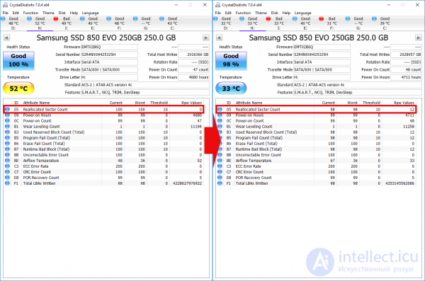
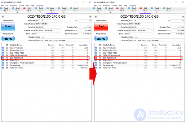
In other words, "aging" processes continue in SSDs even when they are powered off. However, no catastrophic changes occur as a result. The test showed that a relatively long idle period for SSDs that have long since used up their entire rated endurance does not cause them to fail or lose stored data.
But in reality, no one expected anything different. The test was conducted only because some time ago a strange belief began spreading that solid-state drives in a powered-off state very quickly lose their ability to reliably retain data. Moreover, many tech-adjacent sites seriously contributed to spreading this misconception, repeating — and sometimes still stubbornly relishing — the claim that SSDs disconnected from power can lose recorded data within just a few days.
In reality, this problem has been blown out of proportion almost from nothing. Of course, the process of charge leaking out of flash memory cells when a drive is disconnected from power does occur, but it happens much more slowly, and there is no way data could be lost within a matter of days.
As confirmation, one can refer to the specifications of JEDEC — a committee that includes all the leading semiconductor manufacturers and that develops unified standards for products in the microelectronics industry. These standards are, on the one hand, mandatory for manufacturers, and on the other hand, serve as a benchmark for customers, since they describe the main consumer-relevant qualities of devices produced by the industry.
Actually, the source of the panic that arose regarding data retention on powered-off SSDs was a table "taken out of context" from one of this committee's presentations, which listed "retention periods" for data on powered-off drives depending on ambient temperature.
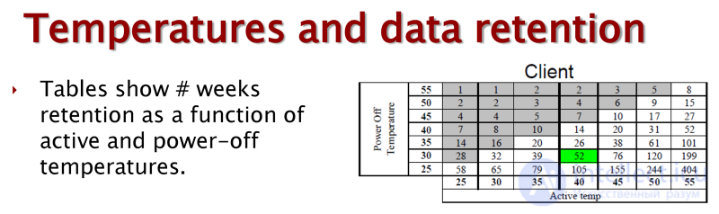
Minimum data retention periods for a powered-off SSD (in weeks)
NAND memory, whose operating principle involves holding electrons in a floating gate, does indeed gradually lose its stored charge while at rest (without periodic refreshing). And sooner or later this can result in the contents of a cell being misinterpreted and data being lost. Our understanding of how and how quickly the charge-leakage process occurs is very well defined and backed by numerous experiments. Accumulated data shows that one of the main factors affecting the stability of NAND cells is their degree of wear. Therefore, a solid-state drive's ability to retain information while powered off depends heavily on what stage of its lifecycle it is at. The numbers given in the table above describe the situation for drives that have used up their rated endurance, not for new ones — and that changes almost everything.
In other words, if we're talking about a new SSD, data on it can be retained for years while powered off (within a normal temperature range). Only when we're talking about a drive that has already used up the endurance set by the manufacturer do the "retention periods" specified in the specification start to take on any real meaning. That is, 52 weeks (a year) is the minimum period of time during which, per specification, a regular consumer drive must retain data while powered off after it has already used up its entire specified endurance. But in reality, the information will most likely be able to survive on a powered-off SSD much longer: as we've seen, manufacturers state rewrite endurance with a large safety margin. And the situation with retention periods is most likely much the same.
If we dig further into the JEDEC specifications, we can find yet another confirmation that even after significantly exceeding the stated rewrite limit, drives are not prone to rapid loss of the information recorded on them. While the minimum retention period for consumer SSDs is set at one year (at a temperature of 30 degrees), for server models — which are usually based on exactly the same flash memory — this time interval is narrowed to 3 months (at a temperature of 40 degrees).
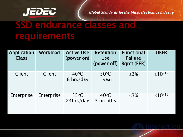
The difference is due to the fact that consumer and server SSDs are assumed to experience workloads of differing intensity. The declared endurance of consumer drives is usually several tens or hundreds of terabytes of rewrites. SSDs belonging to the server class, on the other hand, have a declared reliability that is an order of magnitude higher, reaching units or even tens of petabytes of rewrites. From this it follows that even after writing an amount of data to a regular SSD that significantly exceeds its rated endurance, it will not lose the ability to retain that data while powered off for at least several months — by analogy with the server model.
That's precisely why our two-week check of data integrity in a powered-off state did not reveal any problems. After rewriting hundreds of terabytes, modern SSDs are simply obligated to retain data for much longer than a couple of weeks. And it's quite clear that manufacturers do comply with JEDEC specifications in this regard.
With that, we consider the question of data retention on a powered-off SSD closed. It's clear that testing rewrite endurance is a far more practically important and meaningful experiment, one that can tell us much more about the endurance of modern solid-state drives. Moreover, our testing methodology also checks whether files stored on the SSD at the very beginning of the experiment can still be read correctly.
Nevertheless, we consider it our duty to remind readers that NAND-memory drives are still not intended for archival storage of information. Magnetic storage media — hard drives and tape drives — appear to be a more suitable choice for that purpose. An SSD, on the other hand, is a fast storage medium, aimed primarily at working with "hot" data.
Unfortunately, manufacturers are partly to blame for the fact that some users don't use the full potential of their devices. In official data, a drive's endurance rating may be listed for only some models, tucked away in an obscure corner of the documentation, or missing altogether.
On the other hand, mean time between failures (MTBF) is always present. It might be 1 or 2 million hours, but who cares about that?
This is exactly how uninformative things were with my first solid-state drives, the Kingston V100 — 64 and 128GB. In 2010, these were typical SSDs for ordinary consumers — not the fastest, and relatively inexpensive.
However, the company's website back then had this phrase (the page is gone now).
Recommended workloads for the SSDNow series M, V+ and V is up to 20GB writes per day for three years. For the «E» Series we recommend writes up to 900GB per day for the 32GB and 1.8TB per day for the 64GB SSD.

The endurance of the 64GB drive amounts to 20GB per day over three years, i.e. about 22TB. Note that for the higher-end series it is significantly higher.
That was a long time ago, and those drives have already been discontinued. In the successor series, the Kingston V200 and V300, with the same three-year warranty, it's now clearly stated:
продолжение следует...
Часть 1 Types of SSD Solid-State Drives, Their Parameters, NAND/NOR and SLC/MLC/QLC, Write Endurance, Reliability
Часть 2 How Much Data Gets Written to the Drive - Types

Comments