
Lecture
Shunt — a device that allows electric current (or magnetic flux) to flow around a section of a circuit; it is usually a low-resistance resistor, coil, or conductor.
Shunting — the process of connecting an electrical element in parallel with another element, usually with the aim of reducing the total resistance of the circuit.
First proposed by the American inventor Edward Weston in 1893
Protecting expensive, or hazardous, or non-standardly installed elements of electronic equipment from self-destruction. In the real world there are no two perfectly identical components, even if they come from the same batch — sometimes they need protection even when used together. Subjectively, it seems that the probability of protection tripping at the moment of switching the equipment on/off is higher than during its ongoing operation. For instance, I've seen many exploding capacitors specifically at the moment voltage is applied, and only once an explosion inside a system unit after hours of operation.
Note that there is no such thing as "series shunting" in this article — it discusses how a shunt is connected as part of the overall circuit.
Protecting elements of electronic equipment (distributed electric power networks) by means of shunting is one way of ensuring the safety and reliability of electrical equipment operation. This method is based on using shunts (or bypass) paths to provide an alternative current path and prevent damage to equipment elements when abnormal situations occur.
The basic idea of the method is to create an additional path for the current that bypasses the damaged element. Various components and devices can be used for this, such as fuses, circuit breakers, contactors, and relays. When an abnormal situation occurs, such as a short circuit or overload, the protective elements detect the situation and switch the current onto the alternative path, bypassing the damaged element.
Applying the shunting method makes it possible to prevent serious damage and overloads to equipment elements, which could otherwise reduce the reliability of the system, interrupt the power supply, or even cause a fire. It provides a fast response to abnormal situations and automatic restoration of system operation once the cause of the fault has been eliminated.
It is important to note that the shunting method is one of many methods for protecting electronic equipment elements and can be applied in various combinations with other methods, such as current limiting, isolation, etc., to provide a comprehensive protection system. The specific ways and means of shunting depend on the characteristics and requirements of the particular power supply system.
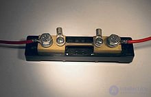
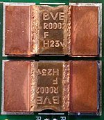
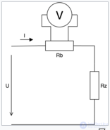
Voltmeter connection diagram
For example, shunts are used to change the upper measurement limit of magnetoelectric ammeters. The required shunt resistance is calculated using the formula:
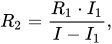
where:
 — shunt resistance, Ohms;
 — ammeter resistance, Ohms;
 — the maximum current that will correspond to full deflection of the instrument's needle, A;
 — the rated maximum current measured by the ammeter without a shunt, A.
If the required measurement limit significantly exceeds the ammeter's rated current, that current in the denominator can be neglected, and the formula then takes the form:
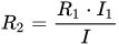 .
.
For example, to measure currents up to 10 A with an ammeter having a resistance of 2000 Ohms and a maximum current of 50 µA, a shunt with the resistance of
 Ohms will be needed.
Using shunts makes it possible to extend the ammeter's reading range (at the cost of degrading the instrument's resolution and sensitivity).
Important notes:
Since circuit simulation programs are not ideally accurate, it is impossible to model the situations described here using them. Moreover, one needs to capture quantities whose duration is measured in microseconds, which is not feasible. Even an environment such as Multisim has caused harm several times already, for example:
Even with such glitches, though, these programs are still needed. They can reveal gross errors precisely in the steady-state operating mode after switch-on: fuses blowing, current and voltage ratings, patterns, and so on. Now let's turn to specific cases of protecting components with shunts, some of which were personally developed.
0. Any shunt is parasitic (with the possible exception of a fuse).
For example, a 0.1 Ohm resistor installed in series with a load takes away from the load exactly the voltage that is measured across it to calculate the circuit current. Hence the rule: for series connection, the shunt's resistance rating is usually small; for parallel connection, it is usually large.
1. Shunting a diode with a resistor — in parallel.
Purpose: preventing high reverse current when several diodes are connected in series.
For example, suppose a diode bridge for 2200V is needed, but only 2D202V diodes rated at 100V are on hand (about 1000 of them at work — they wanted to throw them out, yeah right). So, N diodes are placed in one arm of the diode bridge. Due to physical wear and manufacturing inaccuracies there is a spread in parameters. One of the diodes has a higher internal resistance than the others — its reverse current and reverse voltage will be the highest, as will its forward voltage drop.
If the reverse current exceeds the limit, the diode breaks down, even if the forward voltage limit isn't exceeded. Without a resistor, the reverse currents redistribute onto the remaining diodes — they would all die. With a resistor, the reverse current is redistributed between the resistor and the diode. As a result, the reverse voltage across the diode drops.
Formula for calculating the resistor's resistance: so that 5 times the diode's maximum reverse current flows through it. For example, for the 2D202V at 1mA - 5mA, at a voltage of 10V DC this comes to 0.5kOhm, and at 220V AC it's 15.55kOhm due to the amplitude peak of 311V. A 10-fold maximum reverse current is recommended, though there is no justification for these coefficients. Here, the higher the resistance, the better for the circuit.
Simulation with an alternating voltage showed: if you forget to solder a resistor to one diode, almost the entire forward voltage will drop across that diode, while on the shunted ones it will be around 0.6V.
2. Shunting a capacitor with a resistor — in series.
Purpose:
When a capacitor is about to explode, there is a sharp surge in current: the capacitor's resistance drops, the current rises, the dissipated energy increases, and the resistance drops even further. The electrolyte boils instantly and causes a chemical explosion.
I once made a 1µF/6.3V capacitor explode in practice — this tiny component went off like a medium firecracker and forced me to clean up half the room. Now imagine a 1500µF/500V capacitor exploding — the kind installed in power adapters up to 500V — that's already the equivalent of an explosive device; and if it's Soviet-made, it's a directional one due to the aluminum housing. What's more, it costs 30 dollars (and a 2500µF one costs 60 dollars). At that point it's no longer just about protecting the capacitor, but about preserving your health, your money, the peace of mind of the whole building's neighbors, and the police of the whole district.
So let's not let it explode by installing a current-limiting resistor. The capacitor will then charge for a long time, possibly even seconds (however long it takes for the capacitor to perform its intended function in the circuit) — this needs to be taken into account; this method is not universal.
Since it's impossible to know in advance what current rating the capacitor will have at the moment of explosion, the resistor has to be calculated at the simulation stage. For example, if a smoothing capacitor is installed in a diode bridge, its rating has already been calculated using the formula — meaning the maximum current of the DC source is already known. Connect the maximum permissible load in amps, monitor the voltage ripple across the load, set an acceptable ripple level, and read off the resistor's rating.
Bottom line: instead of a deafening explosion, the capacitor will make a quiet "poof" — it doesn't save it from overvoltage.
3. Shunting a capacitor with a fast-acting fuse — in series (doesn't work!).
Purpose: preventing the capacitor from exploding if the rated voltage is exceeded.
Experiments:
Purpose:
3. Shunting a capacitor with a varistor — in parallel, and a fast-acting fuse — in series.
Purpose: preventing the capacitor from exploding or being destroyed as it approaches its rated voltage.
It simply won't want to explode. The varistor's trip voltage should be a little below the capacitor's rated voltage. The varistor sharply reduces its resistance once it reaches its own limiting voltage, creating what is essentially a short circuit. During the time it takes for the varistor to burn itself out without disconnecting from the circuit, a series-connected fuse of a rating that still allows the capacitor to charge successfully will trip.
Bottom line: no explosion, the capacitor stays intact, the fuse (and, with some probability, the varistor) are destroyed — a trivial price for safety.
4. Shunting a capacitor with a resistor — in parallel.
Purpose: discharging the capacitor so that, after the device is switched off, you don't get an electric shock while working on the device's board.
This is especially relevant for capacitors with a voltage above 42V (above the safe voltage for dry skin per PPB-S regulations). Even at low voltage, the resistor rating comes out to hundreds of kilohms. Recalling past experience: at 3.91V and a resistance of 250kOhm, the capacitor discharged at roughly 0.01V/sec. It's better to charge the capacitor yourself and apply a resistor of a few hundred kilohms. The rating is so high that it has essentially no effect on the circuit's operation, especially if you use megohm values.
5. Shunting a transistor with a diode — in parallel, the diode oriented against the current.
Purpose:
6. Shunting a relay with a diode — in parallel, the diode oriented against the current.
Purpose:
As a result, the relay's release time increases, which can be addressed by installing a resistor in series with the diode. However, as a rule, this delay is so small that it isn't worth paying attention to. The method for calculating the resistor is unknown.
7. Shunting a transistor with a resistor — in series, at the input.
Purpose: equalizing the voltages across parallel-connected transistors at the moment power is applied. An extremely difficult thing to understand — the only things I managed to figure out are:
Absolutely nobody can explain exactly how voltage equalization happens when the transistors turn on with these resistors. Everyone puts on a knowing face and says "just do it this way," but in essence this method remains a pig in a poke that is difficult or impossible to verify by simulation. All that's left is prototyping.
It's also unclear whether such resistors are needed for field-effect transistors, given how extremely fast they turn on (nanoseconds versus microseconds and tenths of a millisecond).
8. Shunting a transistor with a varistor — in parallel.
Purpose: bidirectional protection of the transistor from overvoltage directly during its operation. The varistor doesn't necessarily burn out right away: it can absorb brief voltage spikes without harm to itself, with a response speed of 25ns.
Protecting an electrolytic capacitor with a series diode — to protect against reverse polarity.
Protection from a 10-fold power-supply voltage spike from a choke into the device (after power-off): installing a diode in parallel with the choke, opposite to the supply. At the moment power is switched off, the self-induction EMF, directed in reverse, is fully suppressed by this diode.
I assembled a diode bridge from 32 2D202V diodes (70V/5A), 8 diodes per leg, for use in a 220V DC network. Whether shunted with protective 15.5kOhm resistors in parallel or without them, no difference in performance under load was observed. No excessive difference in diode heating or breakdown was observed either. It's possible this is a coincidence, and the 1986-made diodes happened to come from the same batch, but that seems unlikely. It's also possible the resistors' effect shows up specifically at the peak of the diode bridge's operation — at 5A current — but I don't have that kind of load available for prototyping.
To protect transistors from electromagnetic spikes coming from a relay winding (when switched off), specifically a fast-recovery diode installed in parallel with the relay winding is used. The important parameter of the diode is the maximum reverse recovery time (the diode's ability to accept the next pulse).
(An NPN transistor whose base is connected to GND through a 100kOhm resistor will never pick up interference when the base is disconnected from the positive voltage source. This gets rid of a dangling, unconnected base terminal. The same applies to the other transistors by analogy. 100kOhm is not an optimal value (it's very hard to simulate a random pulsed turn-on of the transistor, but it happened once — and the result was severe overheating of the device).
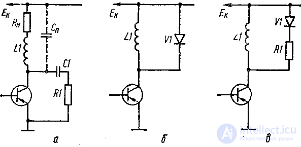
Fig. 2. Circuits for protecting a transistor from overvoltage using: a — a series RC circuit; b — a shunting diode; c — a shunting diode and resistor.
A circuit for protecting transistors from voltage spikes using a shunting diode is shown in Fig. 2,b. In this case, the voltage drop across the inductor equals the forward voltage drop across the diode. The physical meaning of protecting the transistor with a diode is that the energy stored in the inductor is transferred via the diode to the power supply and dissipated in the load's active resistance. To speed up the discharge time, an additional resistor R1 can be connected in series with the diode (Fig. 2,c). Adding resistor R1 also removes high-frequency oscillation of the loop formed by the diode's parasitic capacitance and the inductive load. Instead of R1, a silicon zener diode connected opposite to the shunting diode can also be used (Fig. 3,a). In this case, the maximum voltage across the transistor will be limited to the value UCEmax=Ec+Uz.
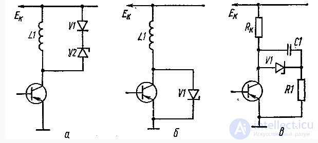
Fig. 3. Circuits for protecting a transistor from overvoltage using: a — a diode and a zener diode; b,c — a zener diode.
To protect amplifiers from random overvoltages as well as from pulsed overloads in circuits with a reactive load, silicon zener diodes are used (Fig. 3,b). In low-frequency amplifiers it's also possible to shunt the collector-emitter section with a diode. In wideband amplifiers, however, this approach can alter the stage's frequency characteristics due to the diode's significant capacitance. The protection circuit used in wideband and other high-frequency amplifiers is shown in Fig. 3,c. The bias is chosen so that it is less than the zener diode's Uz.
Under normal stage operation the zener diode is closed and does not affect the amplifier's frequency response. When the set voltage is exceeded, the zener diode shunts the transistor, protecting it from damage.
To protect the transistor from current overload, the following methods are recommended: installing current-limiting resistors in series with the collector and emitter leads (current should not be limited by installing a resistor in the base circuit); shunting semiconductor devices with a resistor; connecting transistors in parallel. When using the last method, it must be taken into account that semiconductor devices have a spread in resistance, and consequently the current between parallel-connected devices is distributed unevenly. Since the resistance spread depends on temperature and changes over time, reliable operation is achieved either by selecting devices with identical parameters, or by equalizing the devices' currents using small additional resistors connected in series in each device's circuit (Fig. 4). Parallel-connected transistors must be mounted on the same heat sink, taking measures to equalize the temperatures of their cases as much as possible. These temperatures should not differ by more than 1...2°C.
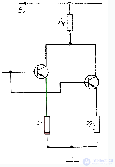
Fig. 4. Circuit for equalizing currents through parallel-connected transistors.
Ensuring the transistor's thermal regime is one of the main tasks when designing radio equipment. Heat-dissipating elements must be designed so that their thermal resistance provides normal heat transfer from the transistor's case to the environment, while the transistor's junction temperature does not exceed the permissible value. When components are freely arranged inside the equipment, it is advisable to use special heat sinks or to mount transistors directly on the device's chassis.
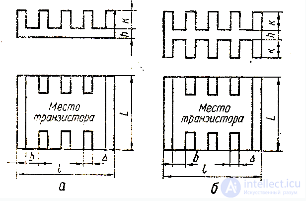
Fig. 5. Finned heat sink; a — single-sided; b — double-sided.
By design, heat sinks are divided into plate-type, single-sided finned, and double-sided finned. The heat-dissipating area can be approximately calculated using the formula
S(cm2)= 1000/(RTj-aσT)
where RTj-a is the required thermal resistance junction-to-ambient, °C/mW; σT is the heat-radiation coefficient from the heat sink to the environment, mW/(cm2 • °C). The coefficient σT is approximately 1.5 mW/(cm2 • °C) and depends on the amount of heat removed from the heat sink via conduction, convection, and radiation. Thermal conductivity increases with the heat sink's area S. Heat removal via convection increases as the temperature difference between the heat sink and the environment grows. Convection improves when the heat sink's plane is positioned vertically. Maximum heat removal via radiation is 0.6 mW/(cm2 • °C). It is recommended to coat the heat sink (radiator) with matte black paint or blacken it by some other means to increase the efficiency of heat removal via radiation.
With densely packed components inside the equipment, or with large dissipated power in the device, using heat sinks located inside the unit or device becomes inefficient. In this case it is advisable to mount powerful transistors directly on the device's housing or on heat sinks that have thermal contact with the external environment.
For efficient heat sink operation, reliable thermal contact with the transistor is required. For this, the surface of the heat sink that contacts the transistor should be flat, smooth, and free of burrs and scratches. A separate hole of minimum diameter should be drilled for each transistor lead. Transistors must be secured to the heat sink using the intended fasteners (bolts, flanges, etc.). To improve thermal contact between the transistor and the heat sink, special heat-conducting pastes or greases are used, for example the KPT-8 silicone thermal paste.
Electrical isolation of the transistor from the heat sink is achieved by installing spacers made of mica, PTFE film tens of micrometers thick, ceramic-metal spacers, or by using heat sinks with deep anodizing. However, one should aim to electrically isolate the heat sink from the device's housing rather than the transistor from the heat sink.
If two or more powerful transistors are connected in parallel, there must be good thermal contact between them so that their thermal regime is uniform and stable. For this, the transistors are mounted on a common heat sink. Otherwise, overheating of one of them will lead to an increase in the power it dissipates due to a decrease in the power dissipated by the others.
METHODS FOR PROTECTING OUTPUT TRANSISTORS FROM OVERVOLTAGE
The need to protect the output transistor from overvoltage arises in a number of specific operating modes of the ignition system. For example, the open secondary-circuit mode is a fault condition, since the amplitude of the primary voltage pulse applied to the "collector-emitter" section of the output transistor increases significantly, which can cause junction breakdown. In addition, the amplitude of the secondary voltage pulse also increases, which can cause insulation breakdown in the ignition transformer's secondary circuit and, consequently, failure of the ignition system. To limit the amplitude of the primary voltage pulse to a level permissible for the output transistor, protection circuits are used, usually built on nonlinear elements — zener diodes and varistors. The simplest one is the circuit shown in Fig. 4.27a.

Fig. 4.27 Ways of connecting a zener diode to protect a transistor from overvoltage:
In this circuit, the protective zener diode VD is connected in parallel with the "collector-emitter" section of transistor VT. The zener diode's breakdown voltage is chosen to be slightly lower than the transistor's maximum permissible Ece. An increase in the primary voltage up to U1 < Uz(VD) does not cause the zener diode to break down. When the primary voltage increases to U1 > Uz, the zener diode breaks down and a current Iz begins to flow through it, limiting the amplitude of the primary voltage pulse to a level permissible for VT. The amplitude of the current pulse through the zener diode is 2-4 A, which requires the use of high-power zener diodes.
a — in parallel with the "collector-emitter" section; b — in parallel with the "base-collector" section.
The development of new power transistors capable of switching large pulse energies (over 200 mJ), together with the desire to reduce the switch's dimensions, made it possible to protect the output transistor by introducing a zener diode in parallel with the "base-collector" section (Fig. 4.27b). This approach reduces the pulse current through the zener diode by a factor of Bstat (Bstat being the output transistor's static current gain).
When the primary voltage increases to U1 > Uz, the zener diode breaks down and current flows into the output transistor's base, partially opening VT for the duration of the overvoltage pulse. The conducting "collector-emitter" section of the transistor shunts the voltage source, thereby limiting the amplitude of the primary pulse to a permissible level.
There are also more complex circuit solutions that allow the pulse current flowing through the zener diode to be reduced even further.
The capacitor connected in parallel with the "collector-emitter" section of the output transistor serves to prevent the transistor from entering avalanche breakdown while it is turning off, and is also an element of the shock oscillatory circuit of excitation, i.e., it determines the magnitude and rate of rise of the secondary voltage developed by the ignition system. Resistor R limits the capacitive current through the transistor's "collector-emitter" section at the moment the latter opens, if the capacitor is charged.
Overvoltage protection: what to choose?
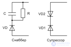
Protection from switching voltage surges in circuits based on thyristors or field-controlled transistors is a routine task in the design of practically any converter. To accomplish this task, there is a range of standard circuits known as snubber circuits. Snubbers, in turn, can consist of passive or active elements, or can combine both (for example, RCD snubbers). Circuits of this kind are well known and require no further discussion. But quite often, when designing snubbers, a number of questions arise regarding component selection.
So, what type of capacitor should you choose? Which is better — a limiter or a varistor? Can
ordinary zener diodes be used instead of specialized limiters? Thus, component-selection questions can significantly affect the resulting snubber circuit, and how, in that case, do you avoid mistakes? Below we will discuss the typical problems with component selection that, as practice shows, most often arise when designing snubber circuits. Snubbers can perform two functions: reducing the rate of voltage rise (C, RC, RCD snubbers) or limiting the amplitude of a voltage spike (snubbers based on suppressors, zener diodes, or varistors). Naturally, the most effective snubbers are those that perform both of these functions. Moreover, snubbers of the second type generally include capacitors in one way or another. The capacitor, in a sense, is the foundation of almost any snubber circuit, and the first question that arises after theoretical calculations is: what type of capacitor should be chosen?
There are two main types of capacitors that, theoretically, can be used in a
snubber: film and ceramic capacitors. Among domestically produced ones, the first group primarily includes the K73 and K78 series; the second group includes the K10 and K15 series. In practice, K78-2 capacitors are considered the most suitable for use as snubbers, but K73-17 is used most often, and ceramic K10-17 or K10-69 capacitors are also frequently used (for relatively low-voltage circuits). There is an opinion that only film capacitors should be used as snubbers, because their parasitic components (especially parasitic inductance and loss tangent) are much smaller than for ceramic capacitors. Comparing the loss tangent: for K78-2 it's 0.001; for K10-69 it's 0.0015; for K73-17 it's 0.008. From this it follows that, apparently, the ceramic capacitor is only slightly worse than the film K78-2 and is even considerably better than the K73-17. If you compare the parasitic inductance of film and ceramic capacitors, there is almost no difference there either: their inductance will range from units to tens of nH and even more, and this parameter is mostly determined by the capacitor's dimensions, lead types, and, ultimately, mounting quality — not by the type.
So it turns out there's no difference? At one time we were tasked with replacing the K73
-17 capacitor with ceramic chip capacitors (a design requirement). As a result, over several years of operation the K73-17 capacitor had zero failures; with ceramic capacitors, there were two failures out of three tests conducted. Hence the conclusion: film capacitors are preferable, but rather not because of
their parameters, but because of their "survivability." Film capacitors are far more resistant to du/dt and di/dt values, to significant pulse currents and overvoltages, and that is precisely why choosing film capacitors is the correct choice.
Of course, in terms of parasitic components too one can say film capacitors are better, but only when talking about specialized capacitors. For example, specialized imported film snubber capacitors have a loss tangent of 0.0001 (an order of magnitude better than K78-2 and almost a hundred times better than K73-17) and their own
inductance of a few nH, but these are specifically special-purpose capacitors. Hence the conclusion: if we're talking about high power (tens of kW and above), then specialized snubber capacitors are unambiguously the choice. If the power is lower but the voltage is relatively high, then general-purpose film capacitors are equally the unambiguous choice; if the power is small and the voltage is low (for example, from experience, at power around a few hundred W and voltage on the order of tens of volts, no problems were observed with snubbers using ceramic capacitors), then ceramic capacitors will suffice. That is, as we can see, the question of capacitor type
is more a matter of reliability; its effectiveness as a snubber, meanwhile, is a matter of calculation and mounting.
A resistor is often (though not necessarily) placed in series with the snubber capacitor. Of course, the resistor's power and rating are calculated, but again, not every
resistor can be used in a snubber circuit. As a rule, the following types of resistors are used: wirewound, metal-film, and carbon. Wirewound resistors are categorically unsuitable for snubber circuits because of their unacceptably high parasitic inductance. Metal-film resistors can be used, although their inductance also leaves something to be desired. The best option is carbon resistors (for example, the C1-4 series). In addition to lower inductance, this type of resistor is favorably distinguished from others by being resistant to pulse currents and overvoltage pulses. That said, using metal-film resistors (the most popular being C2-33) is also acceptable.
As for the diode, if one is used in the snubber circuit, there's probably not much to say, since
it's clear that its breakdown voltage and permissible current must match the circuit, and its reverse recovery time should be as short as possible. Let's move on to the part of the snubber responsible for voltage limiting.
In snubbers, as already mentioned, zener diodes, voltage limiters (suppressors/TVS diodes), and varistors can be installed to limit voltage spikes. What should be chosen, for which circuit, and by what criteria?
The main criteria for choosing a limiting element, besides its breakdown
voltage itself, should be its power and speed. Note that while power can be increased by connecting elements in series, it's not possible to make the speed better than what the manufacturer provides. Of all the limiters presented, the TVS diode (suppressor) has the highest speed.
Suppressor manufacturers claim response speeds on the order of a few ns, and sometimes even less. But that's in test circuits. In practice, even though a suppressor reacts almost instantly, it still takes a relatively long time to fully turn on, and the time from when the voltage reaches the suppressor's breakdown voltage until the pulse voltage begins to drop is usually around 10 ns and depends largely on the pulse current. In circuits with reverse inductive spikes with currents in the hundreds of Amperes, the time to the start of limiting can be tens of ns, and that is exactly why, incidentally, it is recommended to use voltage limiters together with classic snubbers that provide a reduction in du/dt — otherwise the limiting circuit simply doesn't have time to fully engage. In terms of I-V characteristics, the device almost analogous to the TVS diode is the zener diode. But while a zener diode can be selected close to a TVS diode in terms of power (in terms of permissible pulse power), zener diodes are significantly inferior to TVS diodes in terms of speed. Of course, a zener diode can be used as a limiter, but only at rates of no more than a few kV/µs, whereas TVS diodes can handle rates of voltage change an order of magnitude higher. And whereas previously it made sense to use zener diodes in snubber circuits for special-purpose products (since high-voltage TVS diodes with "acceptance 5" quality certification were not
produced), that need has now disappeared, since some manufacturers have started producing "special-purpose" TVS diodes.
Unlike the TVS diode and the zener diode, the varistor is not an active element in the full
sense of the word, being essentially a specialized resistor. The speed of varistors, as claimed, is on the order of a few tens of ns. For comparison, as already noted, the claimed speed of TVS diodes is around a ns. Thus, a varistor is an order of magnitude slower than a TVS diode. This difference is confirmed by a practical case:
in a transistor converter the voltage limiters were heating up significantly, and it was decided to try varistors instead, since the latter can handle relatively higher power. As a result, while the circuit with limiters got hot but operated without failures, the circuit with varistors failed on the very first power-up. However, the author cannot state the real speed of varistors, since he did not have sufficient experience working
with them. Another, no less critical parameter is the maximum permissible pulse power. Here the varistor ranks first, followed by the TVS diode and the zener diode. Moreover, for equal size and weight, the TVS diode significantly outperforms the zener diode. As a result, the application areas for varistors and TVS diodes become clear: varistors are used in circuits with high pulse power but a (relatively) low du/dt value; TVS diodes are the opposite — used in circuits with high du/dt but short-duration pulses. The first type of converter circuits is thyristor-based converters (high power, du/dt measured in hundreds of V/µs); the second type is IGBT- or MOSFET-based converters, since it is precisely the operation of transistors in switching mode that is characterized by short-duration voltage spikes (no more than hundreds of ns; very rarely µs), but with significant du/dt, up to tens of kV/µs. Thus, if it's a thyristor circuit, use varistors; if it's a transistor circuit, use TVS diodes. Zener diodes can also be used, but only in low-voltage transistor circuits with slow rates of voltage change.
For example, BZX55C18 zener diodes installed in the gate circuit of a field-effect transistor perform no worse at all than symmetrical TVS diodes of the 1.5KE18CA type. As a rule, the choice is obvious. Moreover, in the practice of building snubbers, certain "traditions" have already been established, both in terms of circuit design and in terms of component selection. Of course, if you already have some components on hand and it's not possible or is problematic to acquire different components, then you can put together something of your own from what's available. But when designing, it's still better to plan initially for specialized products, and only if that path proves impractical should you resort to general-purpose components. What exactly to choose and for which circuits has been described above.
The content of this article is purely advisory in nature, is based on personal experience, and, of course, is not a cure-all for every problem. Nevertheless, the recommendations given may help a designer with a task such as choosing components for snubber protection circuits.


Comments