
Lecture
The tunnel field-effect transistor (TFET) is an experimental type of transistor. Although its structure closely resembles that of a metal-oxide-semiconductor field-effect transistor (MOSFET), the fundamental switching mechanism is different, which makes this device a promising candidate for low-power electronics. TFETs switch by modulating quantum tunneling through a barrier instead of modulating thermionic emission over a barrier, as in conventional MOSFETs. Because of this, TFETs are not limited by the thermal Maxwell-Boltzmann tail of the carriers, which limits the subthreshold swing of drain current in MOSFETs to about 60 mV/decade of current at room temperature.
Research on TFETs can be traced back to Stutzer, who in 1952 published the first study of a transistor containing the basic elements of a TFET, controlled by a pn-junction. However, the reported control of surface conductivity was not related to tunneling. The first TFET was described in 1965. Joerg Appenzeller and his colleagues at IBM were the first to demonstrate that current oscillations below the MOSFET limit of 60 mV per decade are possible. In 2004, they reported creating a tunnel transistor with a carbon nanotube channel and a subthreshold swing of only 40 mV per decade. Theoretical work has shown that significant energy savings can be achieved by using low-voltage TFETs instead of MOSFETs in logic circuits.
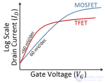
Drain current versus gate voltage for hypothetical TFET and MOSFET devices. A TFET may be able to achieve a higher drain current at low voltages.
In classical MOSFET devices, 60 mV/decade is a fundamental limit on power scaling. The ratio between the on-current and the off-current (particularly the subthreshold leakage, one of the main factors in power consumption) is determined by the relationship between the threshold voltage and the subthreshold slope, for example:

The speed of a transistor is proportional to the on-current: the higher the on-current, the faster the transistor can charge its fan-out (a series capacitive load). For a given transistor speed and maximum allowable subthreshold leakage, the subthreshold slope thus determines a certain minimum threshold voltage. Reducing the threshold voltage is an integral part of the idea of continuous field scaling. Since 2003, the major technology developers have been essentially stuck when it comes to scaling the threshold voltage, and as a result have also been unable to scale the supply voltage (which, for technical reasons, must be at least 3 times the threshold voltage for high-performance devices). As a consequence, processor speed has not advanced as quickly as it did before 2003 (see Beyond CMOS). The emergence of a commercially manufactured TFET device with a slope much lower than 60 mV/decade would allow the industry to continue the scaling trends of the 1990s, when processor frequency doubled every 3 years.
The basic structure of a TFET is similar to that of a MOSFET, except that the source and drain terminals of the TFET are doped with opposite types (see figure). The typical TFET device structure consists of a PIN junction (p-type, intrinsic, n-type), in which the electrostatic potential of the intrinsic region is controlled by the gate terminal.
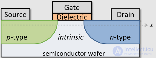
Basic lateral structure of a TFET.
The device operates by applying a gate bias so that electron accumulation occurs in the intrinsic region for an n-type TFET. With sufficient gate bias, band-to-band tunneling (BTBT) occurs, when the conduction band of the intrinsic region aligns with the valence band of the p-region. Electrons from the valence band of the p-type region tunnel into the conduction band of the intrinsic region, and current can flow through the device. As the gate bias is decreased, the bands become misaligned and current can no longer flow.
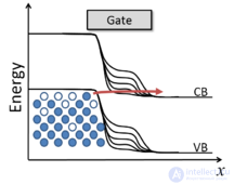
Energy band diagram for the basic lateral TFET structure. The device turns "on" when a sufficient voltage is applied to the gate so that electrons can tunnel from the valence band of the source into the conduction band of the channel.
The group from IBM was the first to demonstrate that current oscillations below the MOSFET limit of 60 mV per decade are possible. In 2004, they reported a tunnel transistor with a carbon nanotube channel and a subthreshold swing of only 40 mV per decade.
By 2010, many TFETs had been fabricated in various material systems, but none had yet been able to demonstrate a steep subthreshold slope at the drive currents required for mainstream applications. At IEDM 2016, a group from Lund University demonstrated a vertical nanowire InAs/GaAsSb/GaSb TFET, which exhibits a subthreshold swing of 48 mV/decade and an on-current of 10.6 µA/µm for an off-current of 1 nA/µm at a supply voltage of 0.3 V, showing the potential to outperform Si MOSFETs at supply voltages below 0.3 V.
Double-gate, thin-body quantum-well-to-quantum-well TFET structures have been proposed to overcome some of the problems associated with the lateral TFET structure, such as the need for ultra-sharp doping profiles; however, such devices may suffer from gate leakage due to large vertical fields in the device structure.
Modeling carried out in 2013 showed that TFET transistors using InAs-GaSb could have a subthreshold swing of 33 mV/decade under ideal conditions.
The use of van der Waals heterostructures for TFET transistors was proposed in 2016.

Comments