
Lecture
In the course of the development of microelectronics (ME), the range of integrated circuits has continuously changed. The main type of integrated circuit today is the semiconductor IC. Classification of integrated circuits. Integrated circuits can be classified according to various criteria; here we will limit ourselves to just one. By manufacturing method, and the resulting structure, two fundamentally different types of integrated circuits are distinguished: semiconductor circuits, and film and hybrid circuits.
As a response to the emergence of microprocessor technology, in 1981 GOST 17021-88 introduced four terms.
Microprocessor - a program-controlled device that carries out and manages the process of digital information processing. This device is manufactured on the basis of one or more LSI circuits.
Microprocessor chip - a chip that performs the function of a microprocessor or part of it. A set of these and other chips, compatible in architecture, design, and electrical parameters, is called a microprocessor set (MPS). By analogy with the base LSI set, the base MPS is called the minimum composition of such a set required to build the main units of a microprocessor or controller.
Recently, alongside the development of general-purpose chips, the creation of complex chips has become widespread, in the development and production organization of which both the customer enterprise and the contractor enterprise take part. The division of work between these enterprises is regulated by GOST 27394-87.
Custom integrated circuit - a chip developed on the basis of standard and/or specially created elements and units according to the customer's functional diagram, and intended for specific electronic equipment.
Semi-custom integrated circuit - a chip developed on the basis of base (including gate-array) dies and intended for use in electronic equipment.
Depending on manufacturing technology, ICs are divided into 4 varieties: semiconductor; film; hybrid; combined
The elements of the electrical circuit of semiconductor ICs are formed in the bulk or on the surface of a semiconductor material (substrate). Active and passive elements are formed by introducing a certain concentration of impurities at various depths of the monocrystalline wafer.
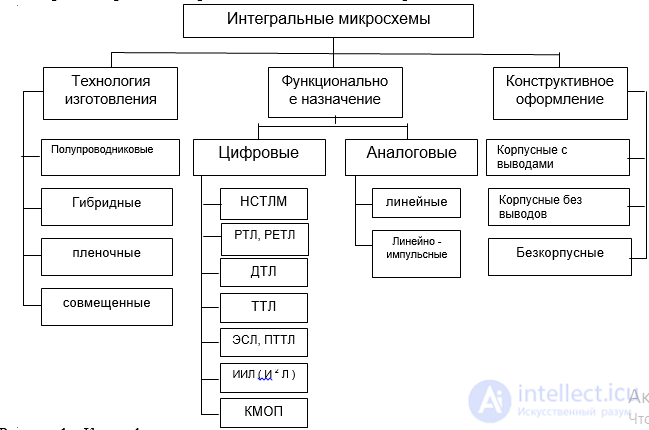
Figure 1 - Classification of integrated circuits
In hybrid ICs, the passive part is made in the form of films deposited on the surface of a dielectric material (substrate), while the active elements, which have their own independent construction, are attached to the surface of the substrate.
Depending on the methods of connecting active chip-scale (uncased) elements, active ICs come with flexible and rigid leads.
A variety of semiconductor ICs are combined ICs.
In combined ICs, the active elements are made inside the semiconductor substrate, while the passive part is made in the form of metal films on its surface.
By functional purpose, ICs can be divided into:
1) digital; 2) analog.
Digital ICs are used in digital computers, discrete automation devices, etc. They include microprocessor circuits, memory circuits, and ICs performing logic functions.
Linear and linear-pulse ICs are used in analog computers and in information conversion devices.
These include various operational amplifiers, comparators, and other circuits.
The classification of digital chips is based on three criteria:
1) the type of logic circuit components on which logic operations are performed on the input variables;
2) the method of connecting semiconductor devices into a logic circuit;
3) the type of connection between logic circuits.
Based on these criteria, logic ICs can be classified as follows:
1) circuits with direct connections on MOS structures - DCTL on MOS (MOS - metal-oxide-semiconductor, or MIS - metal-insulator-semiconductor).
2) circuits with resistor-capacitor connections - RTL; RCTL - circuits whose input logic is implemented using resistor networks. RCTL and RTL are obsolete and are not used in new designs;
3) circuits whose input logic is implemented using diodes - DTL;
4) circuits whose input logic is implemented using a multi-emitter transistor - TTL;
5) circuits with coupled emitters - ECL, or CSL - current-switching logic;
6) injection-integrated logic (I2L) - it is used as the basis for creating high-integration, high-speed chips with low power consumption;
7) circuits based on the joint use of a pair of transistors with channels of different conductivity types, so-called complementary structures (CMOS structures).
In the IC part designation, the design-and-technology implementation is indicated by a digit:
By the nature of the functions performed in electronic equipment, ICs are divided into subgroups (for example, generators, amplifiers, etc.) and types (for example, frequency, phase, voltage converters); the subgroup is designated by corresponding letters (for example, GS - generator (G) of harmonic signals (S), ND - a set (N) of diodes (D))
Chip packages
GOST 17467-88 provides terms relating to IC construction.
Package body - the part of the package without leads.
Lead position - one of several equally spaced lead locations at the point where leads exit the package body, arranged in a circle or in a row, which may or may not be occupied by a lead. Each lead position is designated by a sequential number.
Mounting plane - the plane on which the IC is mounted.
Integrated circuit packages perform a number of basic functions:
-metal-glass (glass or metal base connected to a metal lid by welding, with leads insulated by glass);
-metal-polymer (a substrate with elements and leads is placed in a metal lid, after which it is sealed by filling with a compound);
-metal-ceramic (ceramic base connected to a metal lid by welding or soldering);
-ceramic (ceramic base and lid joined together by soldering);
-plastic (plastic base connected to a plastic lid by molding).
Each type of package is characterized by overall and connection dimensions, the number of leads, and their arrangement relative to the plane of the package base.
Planar IC leads - leads that lie in the plane of the package base. Planar leads are usually rectangular in cross-section.
Pin-type IC leads - leads that are perpendicular to the plane of the package base. Pin-type leads are usually round or rectangular in cross-section.
1 - chip package; 2 - planar lead; 3 - plane of the package base;
4 - pin-type lead; 5 - mounting plane
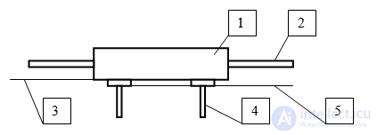
Figure 3 - Schematic representation of a chip package
Microelectronics is a branch of electronics aimed at creating miniature, highly reliable equipment with low power consumption, low cost, and other advantages.
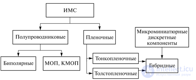
An integrated circuit, or IC for short, is a monolithic product designed to perform the functions of a given stage or an entire system, whose components are interconnected in a specific way and cannot be separated from one another by disassembly operations. There are analog chips, which continuously track and act upon a signal, and digital chips, which discretely convert and process information. Chips are classified by degree of integration, which is equal to the logarithm of the number of parts n placed in a single IC: k = ln n. By manufacturing method, three types of ICs are distinguished: film, semiconductor, and hybrid.
In film ICs, parts and connections are made by producing thin films of small thickness with various properties, formed on a substrate of a non-conductive material. Film chips are divided into two groups: thin-film, with a film thickness of less than 1 micron, and thick-film, with a greater thickness, often on the order of 20 microns. The difference between thin-film and thick-film ICs lies not only in the numerical thickness of the films, but above all in the technology of their deposition.
In semiconductor ICs, parts and connections are formed by special technological methods within a semiconductor crystal. A combined semiconductor IC is one in which some of the parts are made using thin-film technology and another part using semiconductor technology.
In hybrid ICs, abbreviated as HICs, resistors and some other passive components are produced on a dielectric substrate using thin-film technology, while discrete uncased active components are placed nearby on the substrate and connected by wire to contact pads.
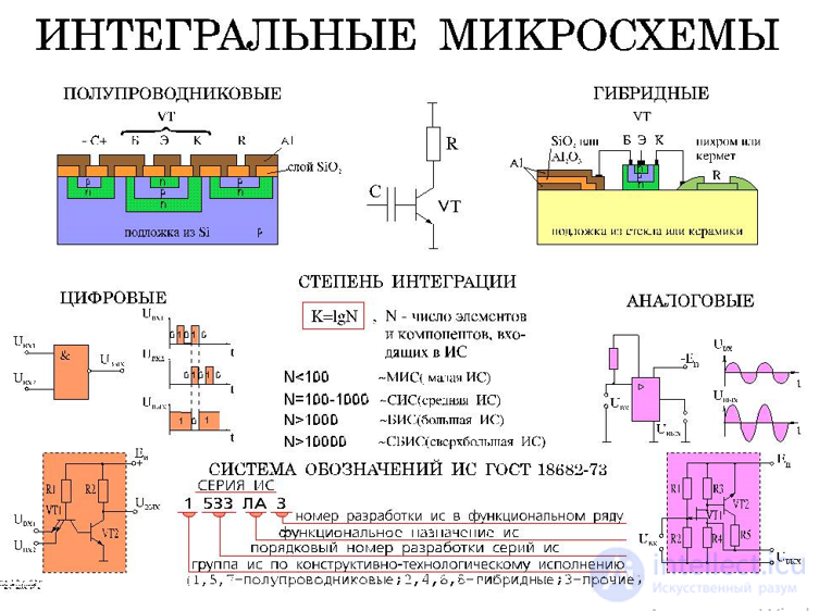
Substrates of semiconductor chips are usually made of p-type monocrystalline silicon. The electron-hole junctions of semiconductor ICs are usually produced by epitaxial growth or by diffusion-planar technology. Planar technology involves creating parts and electrical connections in the substrate within a single plane. Epitaxial growth consists of depositing heated semiconductor material onto certain areas of the substrate surface. Diffusion technology consists of heated gaseous impurities penetrating into designated areas of the substrate. This results in multilayer formations, each layer of which has a specified type of conductivity. Resistors, capacitors, and other passive components of semiconductor ICs have much larger dimensions than active components such as transistors. To minimize size, diodes in semiconductor ICs are preferably replaced with transistors connected as diodes.
A semiconductor IC is a chip whose elements are formed in the near-surface layer of a semiconductor substrate (Fig. 2). These ICs form the basis of modern microelectronics.
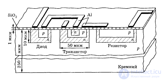
Fig. 2. Structure of elements of a semiconductor IC
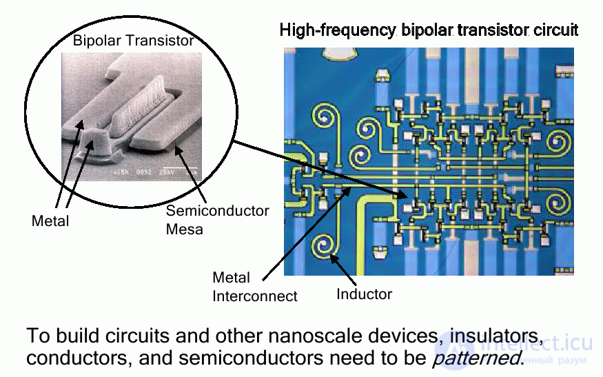
Semiconductor ICs. Currently, the following semiconductor ICs are distinguished: bipolar, MOS (metal-oxide-semiconductor), and BiMOS. The latter is a combination of the first two, combining their positive qualities.
The technology of semiconductor ICs is based on doping a semiconductor (silicon) wafer alternately with donor and
acceptor impurities, as a result of which thin layers with different types of conductivity form beneath the surface, along with p-n junctions at the layer boundaries. Individual layers are used as resistors, and p-n junctions in diode and transistor structures.
Doping of the wafer has to be carried out locally, that is, in separate areas separated by sufficiently large distances.
Local doping is carried out using special masks with openings, through which impurity atoms penetrate the wafer at the
required areas. In the manufacture of semiconductor ICs, the role of the mask is usually played by a film of silicon dioxide SiO2, which covers the surface of the
silicon wafer. In this film, the necessary set of openings of various shapes is etched by special methods, or, as they say,
the necessary pattern (Fig. 4). Openings in masks, in particular in the oxide film, are called windows.
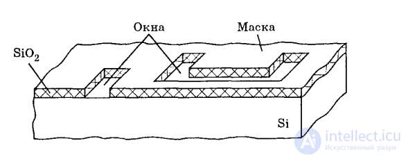
Fig. 4. Oxide mask with windows for local doping
Now let us briefly characterize the constituent parts (elements) of semiconductor ICs. The main element of bipolar ICs is the n-p-n transistor: the entire technological cycle is oriented toward its fabrication. All other elements should, if possible, be fabricated simultaneously with this transistor, without additional technological operations.
The main element of MIS ICs is the MIS transistor. The fabrication of other elements is likewise adapted to the base transistor.
Elements of a bipolar IC must be isolated from one another in one way or another so that they do not interact through the crystal.
Elements of a MOS IC do not require special isolation from one another, since interaction between adjacent MOS transistors does not
take place. This is one of the main advantages of MOS ICs compared to bipolar ones.
A characteristic feature of semiconductor ICs is that inductors, and especially transformers, are absent among their elements. This is because no physical phenomenon equivalent to electromagnetic induction has yet been implemented in a solid body. Therefore, when developing an IC, engineers try to implement the required function without using inductors, which in most cases is possible. If an inductor or transformer is essential in principle, they have to be used as attached (discrete) components. The die sizes of modern semiconductor ICs reach 20x20 mm2. The larger the die area, the more complex, more multi-element an IC can be placed on it. With
the same die area, the number of elements can be increased by reducing their size and the distances between them.
The functional complexity of an IC is usually characterized by the degree of integration, i.e., the number of elements (most often transistors) on the
die. The maximum degree of integration is 106 elements per die. Increasing the degree of integration (and, with it, the complexity of
the functions performed by the IC) is one of the main trends in microelectronics.
To quantitatively assess the degree of integration, a conventional coefficient k = lgN is used. Depending on its value,
integrated circuits are called differently: k  2 (N < 100) - integrated circuit (IC);
2  k
k  3 (N < 1000) - medium-scale integrated circuit (MSI);
3 k
k  5 (N < 105) - large-scale integrated circuit (LSI);
k > 5 (N > 105) - very large-scale integrated circuit (VLSI).
Below are the English designations and their meanings:
IC - Integrated Circuit;
MSI - Medium Scale Integration;
LSI - Large Scale Integration;
VLSI - Very Large Scale Integration.
In addition to the degree of integration, another indicator is used - packing density - the number of elements (most often transistors) per unit die area. This indicator, which mainly characterizes the level of technology, currently reaches
500-1000 elements/mm2.
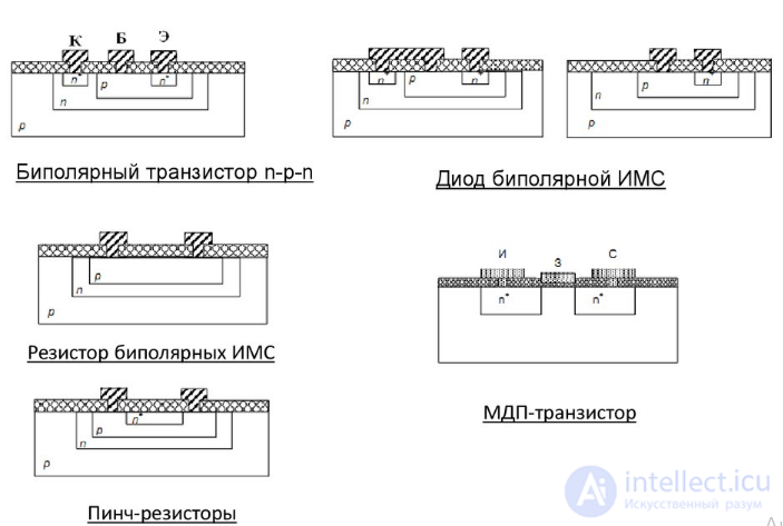
Semiconductor devices (diodes, transistors, field-effect transistors) and semiconductor resistors can be made within a semiconductor crystal. As capacitors with a capacitance of up to 200-400 pF (picofarad, 10^-12) (1 farad equals the capacitance of a capacitor in which a charge of 1 coulomb creates a voltage of 1 volt between its plates), the capacitances of reverse-biased semiconductor diodes are used. The most preferable elements are those that occupy the smallest area on the die - primarily MIS-type field-effect transistors, followed by other semiconductor devices.
Capacitors of larger capacitance and magnetic elements (chokes, transformers) cannot be implemented as part of semiconductor ICs.
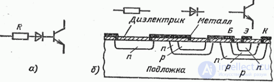
Figure 1. Circuit fragment and its implementation as a semiconductor IC
Resistors of semiconductor integrated circuits are sections of doped semiconductor with two leads. The resistance of such a resistor depends on the resistivity of the semiconductor and the geometric dimensions of the resistor. Resistor resistances usually do not exceed a few kilohms. As higher-resistance resistors, the input resistances of emitter followers are sometimes used, which can reach tens or even hundreds of kilohms. The temperature stability of such resistors is satisfactory over the entire operating range. The deviation of a resistor's resistance from its nominal value is ±20% or more.
Diffused resistors are created in the base or emitter region. They are manufactured simultaneously with the base or emitter region.
The role of capacitors in semiconductor integrated circuits is played by the depletion layers of p-n junctions, reverse-biased by a constant voltage, or by a silicon oxide film. The role of the plates is played by doped semiconductor regions or metal films. The maximum practically achievable capacitance of such capacitors lies within 100-200 pF, and in many chips it is limited to 50 pF, due to the small area of the p-n junctions used (typically 0.05 mm2 or less). The deviation of a capacitor's capacitance from its nominal value is usually ±20%.
The drawback of MIM capacitors and MIS capacitors compared to diffused capacitors is irreversible failure in the event of dielectric breakdown.
As capacitors in integrated circuits, the barrier capacitance of a reverse-biased p-n junction is often used. Such a passive element of an integrated circuit is conveniently formed simultaneously with the formation of transistor structures, or the p-n junctions of transistor structures themselves can be used directly. The barrier capacitance of a p-n junction can be used both to create a fixed-capacitance capacitor and a variable capacitor, which can be controlled by changing the constant bias across the junction.
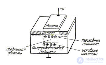
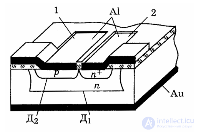
Fig. 7.2 Structural diagram of an integrated capacitor based on a p-n junction.
Diffusion is used to form p-n junctions, so capacitors based on them are called diffused capacitors. The structure of such a capacitor is shown in Fig. 7.2, where the numbers 1 and 2 denote ohmic contacts. The operating principle of diffused capacitors is based on using the barrier capacitance of a reverse-biased p-n junction, where the dielectric is the depletion layer of the p-n junction.
The equivalent circuit of a capacitor based on a collector p-n junction is shown in Fig. 6.3, where C1 is the barrier capacitance of the collector junction, and C2 is the parasitic capacitance of the isolating collector-substrate junction. It has limited application, since the substrate lead is common to the whole IC and is grounded with respect to the AC component of the current. Capacitor C2, however, is an integral part of the integrated circuit, since it is always present when circuit elements are isolated by a
p-n junction. Diodes D1 and D2 form capacitances C1 and C2. R is the resistance characterizing the non-ideality of the dielectric and the presence of bulk resistance in the p-layer.
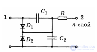
Fig. 7.3 Equivalent circuit of an integrated capacitor based on a p-n junction.
For effective use of the capacitor, i.e., to obtain the maximum signal transfer coefficient through the capacitor to the load, the ratio C1/C2 must be as large as possible. This is achieved with a low reverse bias of the base-collector junction and a high bias voltage of the collector-substrate junction, which allows C1/C2 to be obtained in the range of 3 to 10. The approximate maximum capacitance of a diffused capacitor is about 500 pF. The maximum allowable operating voltage lies in the range from -15 to -25 V.
The resistance R affects the quality factor of the capacitor, which is determined by the relation
 . (7.4)
As the resistance of this or any resistor connected in series with the capacitor increases, its quality factor decreases.
Such a capacitor is polar. Its capacitance changes depending on the value of the applied voltage. The maximum capacitance value occurs when the external bias voltage is zero. The capacitance is determined by the contact potential difference. However, this mode of operation of the capacitor is rarely used in practice.
In semiconductor integrated circuits, either two-layer structures with a single p-n junction, or transistors connected as diodes, are used as diodes
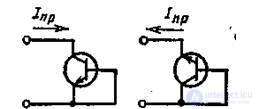
Diode connection of transistors
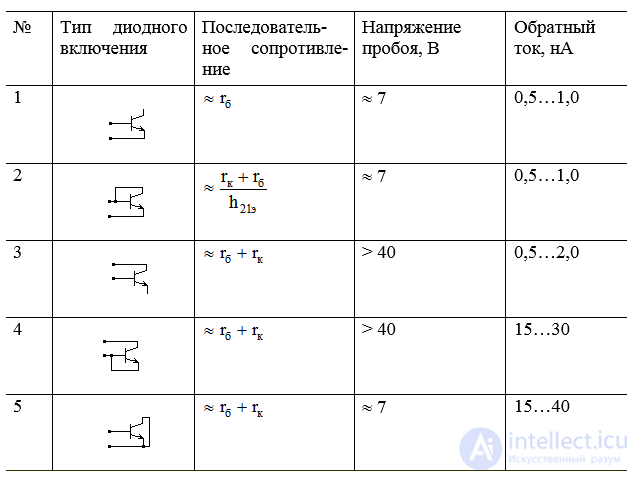
Five possible ways of connecting an integrated transistor to form a diode:
Table 7.1 also gives some parameters of integrated diodes.
Table 7.1
An important parameter characterizing the speed of a transistor is the excess charge storage (recombination) time. To reduce it, the integrated transistor is doped with gold, which has a high diffusion coefficient and penetrates all regions of the transistor (base, emitter, collector). This creates additional recombination centers. As a result, the lifetime of minority carriers in the base decreases, and the current transfer ratios h21e and h21b decrease. To maintain high values of h21e and h21b while reducing the storage time, the base-collector junction is shunted with a Schottky diode. Such transistors are called Schottky-barrier transistors. Unlike a planar transistor, in Schottky-barrier transistors the base contact opening is extended toward the n-type collector region (Fig. 7.10,a). The Schottky diode is formed at the point of contact between the metal and the high-resistance n-type collector region. The Schottky diode turns out to be connected in parallel with the collector junction (Fig. 6.10,b).
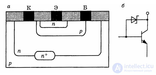
Fig. 7.10 Structural diagram (a) and symbol (b) of a Schottky-barrier transistor.
In cutoff mode and in active mode, the collector potential is higher than the base potential, the Schottky diode is closed, and the transistor operates as an ordinary bipolar transistor. When switching from active mode to saturation, the collector potential becomes lower than the base potential. The Schottky diode opens, and most of the base current flows into the collector through the Schottky diode, bypassing the base region of the transistor. In this case, no excess charge accumulates in the base region, and when the transistor switches from saturation to active or cutoff mode, there is almost no excess charge storage (recombination) process. The excess charge storage time is determined by the electron transit time through the base and, for transistors with a sufficiently thin base of less than 1 micron, does not exceed 1 ns.
The main application area for transistors with a Schottky diode is high-speed digital chips, where the transistors operate in saturation mode. In addition to the storage time, the switching speed of a transistor in pulse mode is strongly affected by the delay, rise, and fall times, which are determined by the barrier capacitances of the junctions and the load capacitance. The use of transistors with a Schottky diode can increase the speed of digital chips by 2 to 5 times.
Digital integrated circuits widely use special transistor structures - multi-emitter transistors - which have no discrete analog. Multi-emitter n-p-n transistors (METs) differ from single-emitter transistors in that several emitter regions (usually 4 to 8) are created in their p-type base region. MET structures are obtained in the same technological process used to manufacture ICs, together with single-emitter integrated transistors. A multi-emitter transistor can be represented as a set of individual n-p-n transistors, the number of which equals the number of emitters (Fig. 6.11,a), and which share a common collector and base.
Under each emitter lies an active region of the base, and between adjacent emitters lies a passive region. Adjacent emitters, together with the passive base region separating them, form a lateral parasitic n-p-n transistor. The role of the collector in the parasitic transistor is played by the emitter to which a negative voltage is applied. To eliminate this parasitic phenomenon, the distance between adjacent emitters of the MET is made greater than the diffusion length of minority carriers in the base.
The MET is connected according to the circuit shown in Fig. 7.11,b. The MET is used to create transistor-transistor logic chips. In integrated circuits, the inverse connection of the MET is often used, in which case the transistor is called a multi-collector transistor (MCT). The multi-collector transistor is used in integrated circuits with injection power supply.
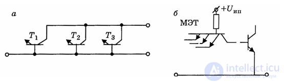
Fig. 7.11 Multi-emitter transistor (a) and its connection diagram (b).
Interconnections in an IC should have a minimum number of crossings and minimum length of conducting traces. If crossings cannot be avoided entirely, they can be implemented by using capacitor plates, forming additional contacts to collector regions of transistors, using diffused jumpers, and finally, by creating an additional insulating layer between crossing conductors;
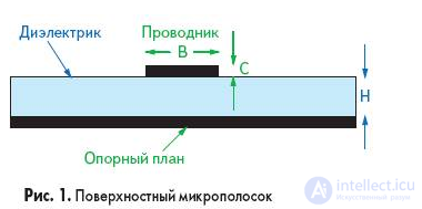
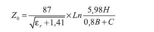
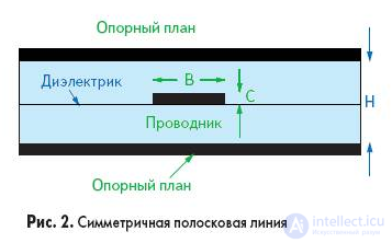
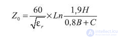
The characteristic impedance depends on the conductor width B, the conductor thickness C, the thickness of the dielectric layer, and the dielectric permittivity of the dielectric E.
A combined IC is a chip in which the active elements are made in the near-surface layer of the semiconductor crystal (as
in a semiconductor IC), while the passive elements are deposited in the form of films on a pre-insulated surface of the same crystal (as in a
film IC).
Combined ICs are advantageous when high nominal values and high stability of resistances and capacitances are required; these requirements are easier to achieve with film elements than with semiconductor ones.
In all types of ICs, interconnection of elements is achieved using thin metal strips deposited or applied onto the
surface of the substrate and making contact where needed with the elements being connected. The process of depositing these interconnecting
strips is called metallization, and the "pattern" of interconnections itself is called metal wiring.
Substrates of film chips, which are made of sapphire, glass-ceramics, ceramics, and other materials, always have a rectangular shape and a thickness of about 0.2 mm to 1 mm. Substrates must not undergo chemical reactions with the film materials, must have a low degree of surface roughness, and must have high electrical resistance. Films are deposited onto the substrate through a stencil called a mask. Making film capacitors, and especially inductors, is not recommended for very significant reasons, although in some cases they cannot be avoided.
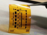
Thick-film contact pads are made, for example, by firing pastes containing aluminum, copper, tantalum, or, in rare cases, gold. To improve the adhesion of metal coatings to the substrate, an intermediate nickel layer, which has better adhesion than other metals, is first formed on it, and only then is the required material deposited on this layer.
Film resistors, which are made by depositing pastes containing nickel, cermets, tantalum, chromium, etc. with a binder onto the substrate, have a rectangular shape. To increase the resistance of the resistor, it is made in the form of numerous interconnected identical elementary sections of L-shaped or U-shaped configuration, which are repeated until the required resistance is obtained, as shown in Fig. 1.
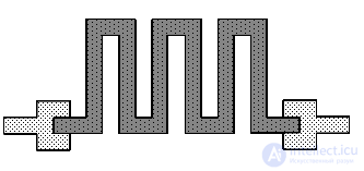
Fig. 1 Film resistor
Usually the resistance of such a film resistor can range from 0.05 kOhm to 50 kOhm, and it is difficult to obtain a much higher or much lower resistance.
Resistors in thin-film ICs are either a strip or a film of a certain configuration, deposited between two contacts on an insulating substrate. Fig. 7.1,a,b show configurations of film resistors.
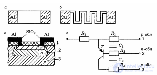
Fig. 7.1. Simplified construction of film resistors (a,b), structural and equivalent circuit.
Film capacitors have a multilayer structure and are generally formed by two electrically conductive films, between which a dielectric film layer is placed. The plates of film capacitors are made from electrically conductive films containing aluminum, tantalum, silver, copper, and similar materials. The dielectric film is usually obtained from various oxides: tantalum oxide, antimony trisulfide, silicon dioxide, germanium monoxide, etc. The capacitance of film capacitors is usually from 10 pF to 20 nF.
Film inductors have a spiral shape, as shown in Fig. 2, and are formed by depositing conductive films onto the surface of the substrate.
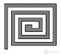
Fig. 2. Film inductor
The inductance of such film coils does not exceed 10 microhenries.
Manufacturing active components by layering films presents great difficulties.
A film IC is a chip whose elements are made in the form of various types of films deposited on the surface of a dielectric substrate (Fig. 3). Depending on the deposition method and the associated film thickness, thin-film ICs (film thickness up to 1-2 microns) and thick-film ICs (film thickness from 10-20 microns and above) are distinguished.
Since no combination of deposited films has yet made it possible to obtain active elements such as transistors, film ICs
contain only passive elements (resistors, capacitors, etc.).
Therefore, the functions performed by purely film ICs are extremely limited. To overcome these limitations, a film IC is supplemented with active components (individual transistors or ICs), placing them on the same substrate and connecting them to the film elements. This results in an IC called a hybrid IC.
Usually, purely passive parts, such as fixed resistors, are created on the dielectric substrate of a hybrid IC (HIC). Active discrete components designed for use in HICs are uncased, and to protect them from harmful environmental effects, they are coated with drops of varnish or compound. Active components are transported in special containers. Contact pads created on the HIC substrate are needed to provide interconnections between film parts, as well as for connecting thin wires that make electrical contacts between the thin-film and external discrete components. The active components connected to the contact pads are made with either rigid or flexible leads. Parts with rigid leads are most convenient for automatic assembly of HICs, but developing such products involves certain difficulties. Capacitors with a capacitance greater than 20 nF and inductors are usually not made on the HIC substrate, but are used as attached (discrete) components. In large HICs - abbreviated LHICs - uncased semiconductor chips are used as external parts. The components of an HIC are connected to the package leads by soldering, microwelding, etc.
Hybrid ICs. Film ICs, and hence hybrid ICs, are divided into thick-film and thin-film types depending on the manufacturing technology.
Thick-film HICs (let us denote them TkHIC) are manufactured quite simply. Pastes of various compositions are applied onto a dielectric substrate plate. Conductive pastes provide interconnections between elements, capacitor plates, and leads to the package pins; resistive pastes provide resistors; dielectric pastes provide insulation between capacitor plates and overall protection of the surface of the finished HIC.
Each layer must have its own configuration, its own pattern. Therefore, when making each layer, the paste is applied through its own mask - a stencil - with openings in the places where the paste of that layer should go. After this, the attached components are glued on and their
leads are connected to the contact pads.
Thin-film HICs (let us denote them TnHIC) are manufactured using more complex technology than TkHICs. Classical thin-film technology is characterized by films being deposited onto the substrate from the gas phase. After growing each successive film, the chemical composition of the gas is changed, thereby changing the electrophysical properties of the next film. In this way, conductive, resistive, and dielectric layers are obtained in turn. The configuration (pattern) of each layer
is determined either by a stencil, as in the case of TkHICs, or by a mask, similar to the oxide mask in semiconductor ICs (Fig. 4).
Attached elements in TnHICs, as in TkHICs, are glued onto the surface of the finished film part of the circuit and connected to the corresponding contact pads of the elements. The degree of integration of an HIC cannot be assessed in the same way as for semiconductor ICs. Nevertheless, there is a term "large HIC"
(or LHIC), which means that the attached components in the HIC are not individual transistors but entire semiconductor ICs.
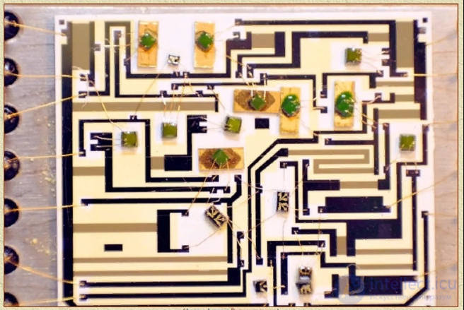
K816UD2V operational amplifier
A hybrid IC (or HIC) is a chip that represents a combination of film passive elements and active
components located on a common dielectric substrate. The discrete components included in a hybrid IC are called
attached components, emphasizing their separateness from the main technological cycle used to produce the film part of the circuit.
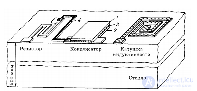
Fig. 3. Structure of elements of a film IC: 1 - upper plate; 2 - lower plate; 3 - dielectric; 4 - connecting metal strip
Another type of "mixed" IC, combining semiconductor and film integrated elements, is called a combined IC.

Comments