
Lecture
Transistor-transistor logic (TTL) is a class of digital logic integrated circuits built on bipolar transistors and resistors. The name transistor-transistor arose because transistors are used both to perform logic functions (such as AND, OR) and to amplify the output signal (unlike resistor-transistor logic and diode-transistor logic).
The simplest basic TTL element performs the logical NAND operation. It essentially repeats the structure of DTL chips while, through the use of a multi-emitter transistor, combining the properties of a diode and a transistor amplifier, which increases speed, reduces power consumption, and improves the chip manufacturing process.
TTL became widely used in computers, electronic musical instruments, and also in measurement and control instrumentation and automation equipment. Because of its widespread use, the input and output circuits of electronic equipment are often made electrically compatible with TTL. The maximum voltage in TTL circuits can reach 24 V, but this leads to a high level of parasitic signal. A sufficiently low level of parasitic signal while maintaining adequate efficiency is achieved at a voltage of 5 V, which is why this value became part of the TTL technical standard.
TTL became popular among electronic system designers after Texas Instruments introduced the 7400 series of integrated circuits in 1965. This series became an industry standard, but TTL chips are also produced by other companies. Moreover, Texas Instruments was not the first to begin producing TTL chips — Sylvania and Transitron had started somewhat earlier. Nevertheless, it was Texas Instruments' 74 series that became the industry standard, largely due to the company's large production capacity and its efforts to promote the 74 series. Since Texas Instruments' bipolar 74-series ICs became the most widespread, they are functionally and parametrically replicated by other manufacturers' products (Advanced Micro Devices, Fairchild's 90/9N/9L/9H/9S series, Harris, Intel, Intersil, Motorola, National, and so on).
The importance of TTL lies in the fact that TTL chips proved to be more suitable for mass production while also outperforming previously produced series of chips (resistor-transistor logic and diode-transistor logic) in their parameters.
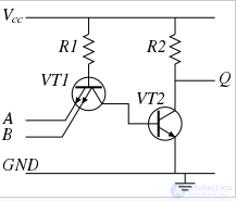
Operating principle of TTL with a simple inverter:
Bipolar transistors can operate in the following modes: cutoff, saturation, normal active, and reverse active. In the reverse active mode, the emitter junction is closed while the collector junction is open. In the reverse active mode, the transistor's current gain is significantly lower than in normal mode, due to the asymmetry in the design of the base-collector and base-emitter junctions — in particular, due to differences in their areas and the doping levels of the collector and emitter semiconductor layers (for more on the operating modes of a bipolar transistor, see Bipolar Transistor).
When the potential at any emitter of the multi-emitter transistor VT1 is zero, it operates in normal saturation mode, since current from resistor R1 flows into the base, so the potential at the collector of VT1 and the base of VT2 is close to zero (Vbe1 = (A|B=0) + 0.7V ≱ Vbc1 + Vbe2, as described in this article in English), which puts VT2 into cutoff mode. Therefore, the potential at the collector of VT2 is close to the supply voltage Vcc — the element's output is logic 1. In this state, a change in the potential of another emitter does not change the state of the element. Through the emitter (input) connected to "ground," a current I = (Vcc — 0.7)/R1 flows to ground, where 0.7 V is the voltage drop across the forward-biased emitter junction of VT1.
If all emitters are disconnected, or a logic 1 voltage (more than 2.4 V) is applied to them, then current from resistor R1 flows through the forward-biased collector junction of VT1 into the base of VT2, I = (Vcc — 1.4)/R1, where 1.4 V is the sum of the voltage drops across the forward-biased emitter junction of VT2 and the forward-biased collector junction of VT1. In this case VT2 enters saturation, and its collector potential becomes close to zero (logic 0).
Thus, the output will be logic 0 only if all inputs are at logic 1, which corresponds to the NAND logic function.
TTL has increased speed compared to DTL logic, even if the transistors used have equal speed. This is because, when the output transitions from logic zero to logic 1, the transistor comes out of saturation, and the minority carriers accumulated in the base of VT2 not only recombine spontaneously but also drain into the collector of the saturated VT1 (whose potential, as mentioned earlier, is close to zero). The typical delay per element in early TTL chip series is about 22 ns.
Some chips in each TTL series are manufactured without the R2 resistor, with the collector of VT2 brought out to the output — the so-called "open-collector" elements. A group of such outputs can be electrically connected together and fitted with a single external resistor, the other end of which is connected to Vcc, thereby implementing the "AND" logic function — such a connection is sometimes called a "wired AND." On circuit diagrams, an additional symbol is used in the schematic designation of open-collector elements.
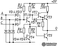
TTL logic (like TTLS) is a direct descendant of DTL and uses the same operating principle. The input TTL transistor (unlike a conventional one) has several emitters, usually from 2 to 8. These emitters act as input diodes (by comparison with DTL). Compared to the assembly of discrete diodes used in DTL circuits, a multi-emitter transistor takes up less chip area and provides higher speed. It should be noted that in TTLS chips, starting with the 74LS series, instead of a multi-emitter transistor an assembly of Schottky diodes is used (74LS series), or PNP transistors combined with Schottky diodes (74AS, 74ALS series), so that in effect there has been a return to DTL. The name TTL is rightfully carried only by the 74, 74H, 74L, and 74S series, which contain a multi-emitter transistor. All later series do not contain a multi-emitter transistor, are in fact DTL, and bear the name TTLS (Schottky TTL) only "by tradition," being in fact a development of DTL.
Transistor-transistor logic with Schottky diodes (TTLS)
TTLS uses Schottky diodes, in which the Schottky barrier prevents the transistor from entering saturation mode, so that the diffusion capacitance is small, switching delays are small, and speed is high. Such a combination (a bipolar transistor with a Schottky diode in the base-collector circuit) is considered a separate component — a Schottky transistor — and has its own designation on circuit diagrams.
TTLS logic differs from TTL in that it has Schottky diodes in the base-collector circuits, which prevents the transistor from saturating, as well as clamping Schottky diodes at the inputs (rarely at the outputs) to suppress pulse interference arising from reflections in long transmission lines (a line is considered "long" when the signal propagation time along it exceeds the duration of its edge; for the fastest TTLS chips a line becomes "long" starting at a length of a few centimeters).
The typical propagation delay (Tpd) and power consumption (Pd) values for each series are given in parentheses, taken from Texas Instruments' document SDAA010.PDF, except for 74F, for which the data is taken from Fairchild's AN-661.
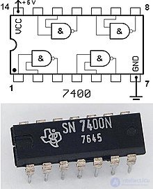
The "74" series prefix denotes the commercial variant of the chips, while "54" denotes the industrial or military variant, with an extended temperature range of −55 °C...+125 °C. The package type is usually indicated by the last letter in the designation; for example, for Texas Instruments, a plastic DIP package is coded with the letter N (SN7400N).
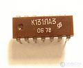
K131LA3, made at the "Elektronpribor" plant, Fryazino
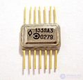
133LA3, military version, made at the "Planeta" plant, Veliky Novgorod
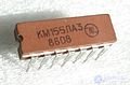
KM155LA3, made at the "Integral" plant, Minsk
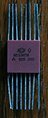
I533KP11, made at the "Svetlana" plant, St. Petersburg
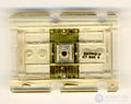
B533TM2 in a chip carrier, made at the "Mezon" plant, Chisinau
During TTL operation, fairly strong current spikes are observed (especially at the output), which can create parasitic interference on the power supply lines, leading to malfunctions of the TTL elements themselves. To combat this phenomenon, the following rules should be followed:
Not all available inputs of a TTL element are always used in a given circuit. If the logic of operation requires a zero signal at the input, the unused inputs are connected to the common wire.
TTLS uses Schottky transistors, in which the Schottky barrier prevents the transistor from entering saturation mode, so that diffusion capacitance is minimal, switching delays are small, and speed is high.
TTLS logic differs from TTL in that it has Schottky diodes in the base-collector circuits, preventing transistor saturation, as well as clamping Schottky diodes at the inputs (rarely at the outputs) to suppress pulse interference arising from reflection in long transmission lines (a line is considered "long" when the signal propagation time along it exceeds the duration of its edge; for fast TTLS chips a line becomes "long" starting at a length of a few centimeters).
TTL devices consume significantly more power than equivalent CMOS devices at rest, but power consumption does not increase with clock frequency as quickly as it does for CMOS devices. Compared to modern ECL circuits, TTL consumes less power and has simpler design rules, but is significantly slower. Designers can combine ECL and TTL devices in a single system to achieve the best overall performance and cost, but level-shifting devices are required between the two logic families. TTL is less susceptible to damage from electrostatic discharge than early CMOS devices.
Because of the output structure of TTL devices, the output impedance is asymmetric between the high and low states, making them unsuitable for driving transmission lines. This drawback is usually overcome by buffering the outputs with dedicated line-driver devices when signals must be transmitted over cables. ECL, thanks to its symmetric, low-impedance output structure, does not have this drawback.
The TTL "totem-pole" output structure often has brief overlap, when both the upper and lower transistors conduct current, resulting in a significant current pulse drawn from the power supply. These pulses can combine unpredictably across multiple integrated circuit packages, reducing noise margin and degrading performance. TTL systems typically have a decoupling capacitor for every one or two IC packages, so that the current pulse from one TTL chip does not instantaneously pull down the supply voltage for another.
Some manufacturers now supply CMOS logic equivalents with TTL-compatible input and output levels, usually with part numbers similar to the equivalent TTL components and with the same pinouts. For example, the 74HCT00 series provides many drop-in replacements for bipolar 7400-series parts, but uses CMOS technology.
Successive generations of technology produced compatible parts with improved power consumption or switching speed, or both. Although vendors uniformly marketed these various product lines as Schottky TTL, some of the underlying circuits, such as those used in the LS family, could more properly be regarded as DTL.
Variants and successors of the main TTL family, which has a typical gate propagation delay of 10 ns and power dissipation of 10 mW per gate, giving a power-delay product (PDP), or switching energy, of about 100 pJ, include:
Most manufacturers offer commercial and extended temperature ranges: for example, Texas Instruments' 7400-series parts are rated for a range of 0 to 70 °C, while 5400-series devices are rated for the military-specification temperature range of −55 to +125 °C.
Special quality levels and high-reliability parts are available for military and aerospace applications.
Radiation-hardened devices (such as those in the SNJ54 series) are offered for space applications.
Before the advent of VLSI devices, TTL integrated circuits were the standard method for building minicomputer and mainframe processors — for example, the DEC VAX and the Data General Eclipse — as well as for equipment such as numerical control of machine tools, printers, and video terminals. As microprocessors became more capable, TTL devices became important for "glue logic" applications, such as fast bus drivers on a motherboard that link together functional blocks implemented in VLSI elements.
Originally designed for processing digital logic-level signals, a TTL inverter can be used as an analog amplifier. Connecting a resistor between the output and the input biases the TTL element as a negative-feedback amplifier. Such amplifiers can be useful for converting analog signals into the digital domain, but would not normally be used where analog amplification is the primary goal. TTL inverters can also be used in crystal oscillators, where their analog amplification capability is significant.
A TTL gate can unintentionally act as an analog amplifier if the input is connected to a slowly changing input signal that crosses the undefined region from 0.8 V to 2 V. The output can become unstable when the input is within this range. Such a slowly changing input signal can also cause excessive power dissipation in the output circuit. If such an analog input must be used, there are specialized TTL components with Schmitt-trigger inputs that reliably convert the analog input into a digital value, effectively acting as a single-bit analog-to-digital converter.

Comments