
Lecture
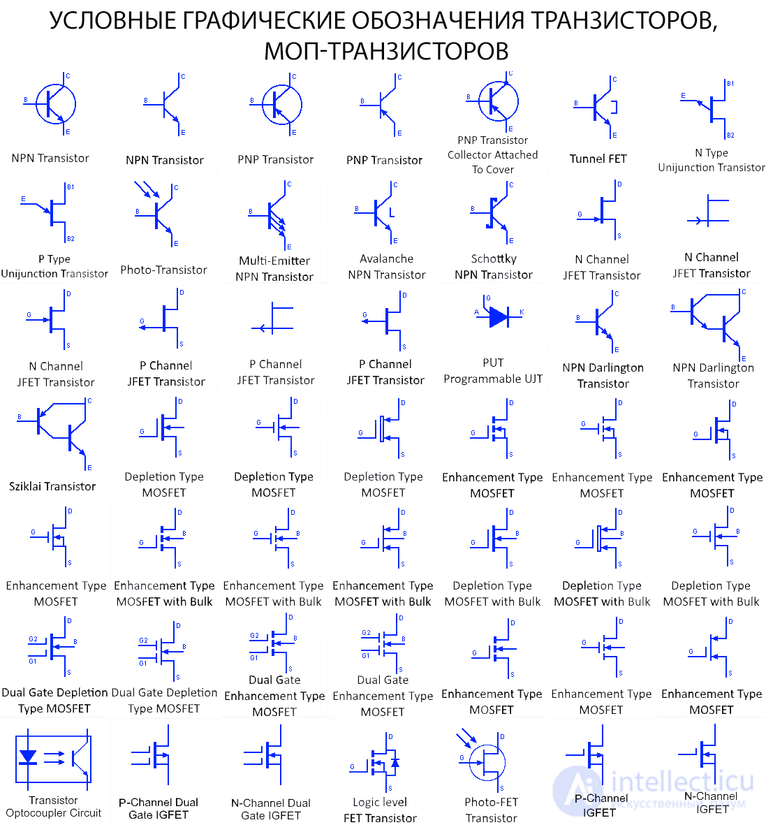
Schematic symbols for transistors and MOSFETs vary depending on their type. Here are the basic symbols:
Bipolar transistor (NPN):
Bipolar transistor (PNP):
N-channel MOSFET:
P-channel MOSFET:
These symbols make it easy to identify transistors in circuit diagrams and understand how they function.
NPN bipolar transistor
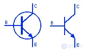
NPN-type bipolar junction transistor (BJT), consisting of 3 layers of semiconductor material. A P-type semiconductor material is located between two N-type materials. It is a current-controlled device used for switching or amplification. The current entering through the base terminal is amplified into the current flowing through the collector.
PNP BJT transistor
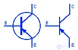
This symbol represents a PNP BJT transistor. It consists of an N-type semiconductor material sandwiched between two P-type materials. The PNP transistor amplifies when its base is negative relative to the collector and emitter. In other words, it amplifies the current flowing out of its base terminal.
Tunnel field-effect transistor

TFET, or tunnel field-effect transistor, is a type of MOSFET whose structure is similar to that of a traditional MOSFET, but whose switching mechanism differs. It uses the phenomenon of quantum tunneling, which makes it an ideal candidate for low-power electronics.
N-type unijunction transistor

Unijunction transistors consist of a lightly doped base with a heavily doped emitter, creating only a single junction. They are also called "double-base diodes." The potential at the emitter relative to the base controls the current through the base. N-type unijunction transistors consist of a lightly doped P-type base (B1 and B2) with a heavily doped N-type emitter (E). They are mainly used for triggering thyristors.
P-type unijunction transistor

This is a P-type unijunction transistor, made from a bar of lightly doped N-type material with a heavily doped P-type section near base 2. Its operation is similar to that of an N-type UJT, but the voltage polarities are reversed,
Phototransistor
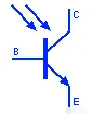
A phototransistor is a light-dependent transistor that converts light energy into an electric current between the collector and emitter. It works similarly to a photodiode, but is more sensitive due to its additional gain. They are used in light-sensitive applications.
Multi-emitter NPN transistor
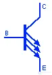
This is a special type of BJT (bipolar junction transistor) that has multiple emitters. The emitters are independent of one another, and the current through each emitter depends on its individual voltage relative to the transistor's base. They are mainly used in TTL (transistor-transistor logic) NAND gates.
Avalanche NPN transistor
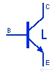
This is a type of BJT specifically designed to operate in the avalanche breakdown region, where the phenomenon of negative differential resistance occurs. At this point, an increase in voltage leads to a decrease in current. Thus, an avalanche transistor has the ability to switch large currents very quickly.
NPN Schottky transistor

It consists of a Schottky diode and a transistor. The Schottky diode is connected between the base and collector. It keeps the transistor from saturating by shunting the excess current. It aids fast switching due to the time delay in removing accumulated charge in saturation mode.
N-channel JFET transistor
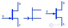
JFETs, or junction field-effect transistors, are unipolar transistors because current flows due to a single type of carrier. JFETs are voltage-controlled, meaning current flows under the influence of the voltage at the gate terminal. The voltage increases or decreases the depletion region that controls the current. An N-channel JFET has an N-type channel between the source and drain, while the gate is made of P-type material.
P-channel JFET transistor
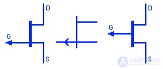
This symbol represents a P-channel JFET (indicated by an arrow pointing outward). A P-channel JFET consists of a P-type channel formed between the drain and source, while the gate is made of N-type material. A P-channel JFET is turned off by maintaining a positive gate-source voltage.
Programmable unijunction transistor (PUT)

A PUT, or programmable UJT, is a four-layer PN device, like thyristors, but it functions as a UJT when programmed with two external resistors. It has an anode, a cathode, and a gate terminal. The voltage at the gate terminal turns the PUT on and off when it crosses the cutoff level.
NPN Darlington transistor pair
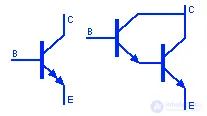
This is a special type of transistor made by connecting the emitter of one BJT to the base of another BJT to increase current gain and sensitivity. It can be made from NPN or PNP transistors connected in this configuration. The overall gain of a Darlington transistor is the product of the gains of the individual BJTs, and the base-emitter voltage drop is twice as large.
Sziklai transistor pair
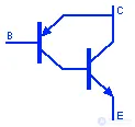
A Sziklai transistor is made from a combination of two NPN and PNP transistors in a Darlington pair. The main advantage of this Sziklai pair is that it turns on at 0.7 V, while the overall gain remains the same as in a Darlington pair.
Depletion-type MOSFET
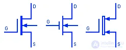
A MOSFET, or metal-oxide semiconductor FET, is another type of field-effect transistor whose gate is completely insulated from the current channel, which is why it is also called an IGFET (insulated-gate FET). It is a voltage-controlled current device. A depletion-type MOSFET is normally on at zero gate-source voltage. It is turned off by applying a positive or negative gate-source voltage for a P-channel or N-channel MOSFET, respectively.
Enhancement-type MOSFET
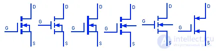
Enhancement-type MOSFETs typically do not conduct current when the gate-source voltage is zero. They turn on when a positive gate-source voltage is applied for the N-channel and a negative gate-source voltage for the P-channel. Enhancement-type MOSFETs resemble normally open switches, whereas depletion-type resembles normally closed switches.
Enhancement-type MOSFET with bulk terminal
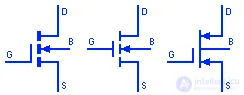
This type of enhancement MOSFET has four terminals. The additional terminal is known as the bulk or body terminal. It is neither an input nor an output terminal, but is used to ground the substrate. It is usually internally connected to the source terminal, so it is omitted from the symbol to show a clearer diagram with less cumbersome wiring.
Depletion-type MOSFET with bulk terminal
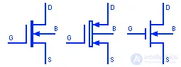
This depletion-type MOSFET has an additional separate terminal for the bulk or body. It is shorted to the MOSFET's source terminal for operation. It grounds the substrate.
Dual-gate depletion MOSFET
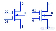
A dual-gate MOSFET is a special type of MOSFET that incorporates two separate gates in series. The gates control the gain more precisely. For example, the gain of the signal at gate 1 can be controlled by varying the signal at gate 2, thereby providing automatic control for signals of varying magnitude.
Dual-gate enhancement-type MOSFET
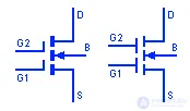
This is a dual-gate enhancement-type MOSFET. It works the same way as a depletion-type MOSFET, but the only difference is that the depletion type is normally conducting, while the enhancement type is normally non-conducting when the gate-source voltage is zero.
Logic-level FET transistor

Logic-level FET transistors are designed for use in digital logic systems. They are used to switch large loads when used with digital logic, meaning that a positive logic voltage of typically 5 V at the gate-source starts conducting maximum current.
Photo FET transistor
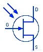
A photo FET transistor is a light-dependent FET that switches when the light intensity at its junction changes. They are used in optocouplers or optoisolators to electrically isolate two circuits by means of an LED between them.

Comments