
Lecture
Plastic or organic electronics generally refers to electronic components based on polymers that act as semiconductors in LEDs and fully replace silicon in microchips.
Organic electronics is a field of materials science concerned with the design, synthesis, characterization, and application of organic molecules or polymers that display desirable electronic properties, such as conductivity. Unlike conventional inorganic conductors and semiconductors, organic electronic materials are created from organic (carbon-based) molecules or polymers using synthetic strategies developed within organic chemistry and polymer chemistry.
One of the promised advantages of organic electronics is its potentially low cost compared with traditional electronics. The attractive properties of polymeric conductors include their electrical conductivity (which can vary depending on the concentration of dopants) and comparatively high mechanical flexibility. Some also exhibit high thermal stability.
One class of materials of interest in organic electronics is electrically conductive materials — that is, substances capable of transmitting electric charge with low resistivity. Traditionally, conductive materials have been inorganic. The classic (and still technologically dominant) conductive materials are metals such as copper and aluminum, as well as many alloys.
The earliest recorded organic conducting material, polyaniline, was described by Henry Letheby in 1862. Serious work on other polymeric organic materials began in the 1960s. In 1963, a high conductivity of 1 S/cm (S = siemens) was reported for a tetraiodopyrrole derivative. In 1977 it was discovered that polyacetylene could be oxidized with halogens to produce conductive materials from what had previously been insulating or semiconducting materials. The 2000 Nobel Prize in Chemistry was awarded jointly to Alan J. Heeger, Alan G. MacDiarmid, and Hideki Shirakawa for their work on conducting polymers. These and many other researchers identified large families of electrically conductive polymers, including polythiophene, polyphenylene sulfide, and others.
In the 1950s, a second class of electrical conductors based on charge-transfer salts was discovered. Early examples were derivatives of polycyclic aromatic compounds. For instance, pyrene was shown to form semiconducting charge-transfer complex salts with halogens. In 1972, researchers discovered metallic conductivity (conductivity comparable to that of a metal) in the charge-transfer complex TTF-TCNQ.
Conductive plastics were developed for industrial applications. In 1987, Ching W. Tang and Steven Van Slyke released the first organic diode at Eastman Kodak.
Bradley, Burroughes, Friend, and colleagues reported the initial characterization of the fundamental properties of polymer light-emitting diodes, demonstrating that the light-emission phenomenon was injection electroluminescence and that the frequency response was fast enough for use in video displays, in a 1990 paper in Nature. The shift from molecular materials to macromolecular materials solved problems previously encountered with the long-term stability of organic films and made it possible to easily obtain high-quality films. As a result of subsequent research, multilayer polymers were developed, and the new field of plastic electronics and organic light-emitting diode (OLED) research and device manufacturing grew rapidly.
In 2000, Alan MacDiarmid of the University of Pennsylvania, Alan Heeger of the University of California, Santa Barbara, and Hideki Shirakawa of the University of Tsukubaruen were awarded the Nobel Prize in Chemistry for being the first to succeed in turning plastic into an electrical conductor. This discovery, together with the results of other research into the electrical properties of organic materials, paved the way for a new kind of electronics based on organic materials.
In 2004, the plastic "Oligotron" was created by the American company TDA Research under contract with the U.S. National Science Foundation. Unlike earlier examples of so-called organic electronics, the new material is distinguished by its insolubility in water.
Before "Oligotron," the best choice of base material for various kinds of organic electronics, such as organic LEDs, was the water-soluble Pedot (poly(3,4-ethylenedioxythiophene)ruen).
Later, Polymer Vision, a Philips "technology incubator," produced a display with a 5-inch diagonal and a bend radius of 2 cm.
Alongside Philips and other leading companies, research was also being carried out by young firms, among them Cambridge Display Technologiesruen (CDT) and Plastic Logicruen — two research companies based at the Cavendish Laboratory of the University of Cambridge.
CDT succeeded in creating LEDs based on polyelectrolytes (PLEDs, a subgroup of organic LEDs, OLEDs), which can be deposited on a moldable and even flexible base, such as PET sheets.
Plastic Logic initially specialized in the use of exotic polymers (semiconductors and conductors) and metals in thin-film transistors (TFTs), which are used in active-matrix backplanes that control displays and perform other functions.
Today, Plastic Logic is the largest company conducting research in the development of plastic electronics and one of the few companies in the world developing polymer backplane technology.
Several different types of conducting and semiconducting polymers are used to create plastic electronics. Plastic Logic uses the services of a number of suppliers, primarily Dow Chemical, which produces poly(3,4-ethylenedioxythiophene)/polystyrene sulfonate (PEDOT/PSS) and poly(9,9-dioctylfluorene-co-bithiophene) (F8T2).
Plastic Logic entered into a cross-licensing agreement with Epson. Siemens created a joint venture with the printing company Kurz. Several leading chemical companies are also involved in this movement.
In January 2011, Rusnano invested $150 million in Plastic Logic, and an agreement was signed to build a plant for the production of next-generation plastic electronics in Zelenograd.
Organic materials fall short of traditional materials in many respects. Modern process technologies make it possible to produce extremely high-density multilayer circuits from silicon (down to process nodes as small as 18 nm). The high number of free carriers in silicon and their low effective mass (compared with available polymers) allow components in silicon microchips to operate at high frequencies, up to the terahertz range (in logic circuits). Even higher frequencies are attainable with gallium arsenide.
Interconnects in traditional process technologies are made of aluminum, copper, and even gold — excellent electrical conductors. The inkjet technologies used in plastic electronics currently rely on polymer compounds or metal-containing conductive pastes, which are markedly inferior to pure metal.
It seems highly doubtful that polymer circuits will, in the foreseeable future, achieve characteristics anywhere close to those of silicon (as of the second half of 2011, the fastest plastic processor has a clock speed of a few kilohertz — millions of times lower than the typical clock speed of silicon processors — and its overall performance lags behind silicon counterparts by nearly a billionfold).
Polymer conductors also degrade faster and are less resistant to ionizing radiation.
Organic materials, for their part, are lighter, more pliable, and easier to shape as needed. Moreover, an essentially unlimited variety of organic materials can be synthesized by swapping out individual building blocks, making it easy to create materials with predetermined properties. A good illustration is full-color displays based on organic LEDs, where the color green appeared several years after the demonstration of the black-and-yellow prototype; the problem of efficient inorganic green LEDs, meanwhile, still has not been solved, owing to the difficulty of forming a semiconductor with the required band gap. The most important advantage of such materials is their low cost compared with silicon counterparts.
A huge advantage of plastic electronics is that it can be manufactured directly, using automated design at very high production speeds. This process creates large, flexible surfaces produced by inkjet printing, without requiring the complex photolithography and vacuum systems needed to create transistors based on crystalline silicon. Inkjet technologies can be reconfigured easily and cheaply (there is no need to produce an extremely expensive set of masks, as with silicon), which is extremely advantageous for small-batch circuits (production runs of under tens of thousands). In principle, every circuit can be unique, which is unthinkable with the traditional photolithography used in the "silicon" process.
Low process temperatures make it possible to use inexpensive substrates and to deposit circuits on the widest possible range of materials.
The drawbacks of plastic semiconductors (namely, the low speed of circuits based on them) are simply irrelevant for many applications, where cost is the decisive factor. Examples of such applications include RFID tags, smart sensors, "smart packaging," electronic paper, and displays, among others.
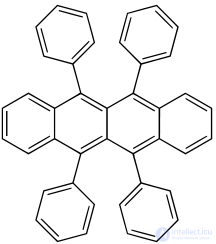
Semiconducting small molecules include polycyclic aromatic compounds such as pentacene and rubrene.
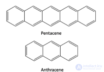
Typical small semiconducting molecules
Electrically conducting polymers are generally either intrinsically conductive or at least semiconducting. In some cases they exhibit mechanical properties comparable to those of ordinary organic polymers. Both organic synthesis and advanced dispersion methods can be used to tune the electrical properties of conducting polymers, unlike typical inorganic conductors. The most thoroughly studied class of conducting polymers includes polyacetylene, polypyrrole, polyaniline, and their copolymers. Poly(p-phenylene vinylene) and its derivatives are used as electroluminescent semiconducting polymers. Poly(3-alkylthiophenes) are also a typical material used in solar cells and transistors.
An OLED (organic light-emitting diode) consists of a thin film of organic material that emits light when stimulated by an electric current. A typical OLED consists of an anode, a cathode, an OLED organic material, and a conductive layer.
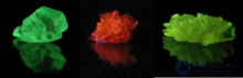
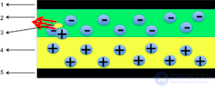
Diagram of a bilayer OLED:
1. Cathode (−),
2. Emissive layer,
3. Emitted radiation,
4. Conductive layer,
5. Anode (+)
André Bernanose [10] [11] was the first person to observe electroluminescence in organic materials, and Ching W. Tang [12] reported the fabrication of an OLED device in 1987. The OLED device featured a bilayer structure consisting of separate hole-transporting and electron-transporting layers, with light emission occurring between the two layers. Their discovery ushered in a new era of ongoing OLED research and device design.
OLED organic materials can be divided into two main families: small-molecule and polymer-based. Small-molecule OLEDs (SM-OLEDs) include organometallic chelates (Alq3), [12] fluorescent and phosphorescent dyes, and conjugated dendrimers. Fluorescent dyes can be selected according to the desired emission wavelength range; compounds such as perylene and rubrene are commonly used. More recently, Dr. Kim J. et al. [13] at the University of Michigan reported a pure organic light-emitting crystal, Br6A; by modifying its halogen bonding, they were able to tune its phosphorescence to different wavelengths, including green, blue, and red. By altering the structure of Br6A, scientists are attempting to create the next generation of organic light-emitting diodes. Small-molecule-based devices are typically fabricated by thermal evaporation in vacuum. Although this method allows the formation of a well-controlled, uniform film, it is limited by high cost and limited scalability. [14] [15]
Polymer light-emitting diodes (PLEDs), similar to SM-OLEDs, emit light under an applied electric current. Polymer-based OLEDs are generally more efficient than SM-OLEDs, requiring comparatively less energy to produce the same luminescence. Common polymers used in PLEDs include derivatives of poly(p-phenylene vinylene) [16] and polyfluorene. The emitted color can be tuned by substituting different side chains onto the polymer backbone or by changing the stability of the polymer. Unlike SM-OLEDs, polymer-based OLEDs cannot be fabricated by vacuum deposition and must instead be processed using solution-based methods. Compared with thermal evaporation, solution-based methods are better suited to producing large-area films. Zhenan Bao [17] et al. at Stanford University reported a new method for producing large-area, thin organic semiconductor films using aligned single-crystal domains.
An organic field-effect transistor is a field-effect transistor that uses organic molecules or polymers as its active semiconducting layer. A field-effect transistor (FET) is any semiconductor device that uses an electric field to control the shape of a channel of one type of charge carrier, thereby changing its conductivity. The two main classes of field-effect transistors are n-type and p-type semiconductors, classified according to the type of charge. In the case of organic field-effect transistors (OFETs), p-type OFET compounds tend to be more stable than n-type compounds, owing to the latter's susceptibility to oxidative damage.
J. E. Lilienfeld [18] first proposed the field-effect transistor in 1930, but the first OFET was not reported until 1987, when Koezuka et al. built one using polythiophene, [19] which exhibits extremely high conductivity. Other conducting polymers have since been shown to act as semiconductors, and newly synthesized and characterized compounds are reported weekly in leading research journals. There are numerous review articles documenting the development of these materials. [20] [21] [22] [23] [24]
As with OLEDs, OFETs can be divided into small-molecule systems and polymer-based systems. Charge transport in an OFET can be quantified using a metric called carrier mobility; currently, rubrene-based OFETs exhibit the highest charge carrier mobility, at 20–40 cm2/(V·s). Another popular OFET material is pentacene. Because of its low solubility in most organic solvents, it is difficult to fabricate thin-film transistors (TFTs) from pentacene itself using conventional spin-coating or dip-coating methods, but this obstacle can be overcome using a TIPS-pentacene derivative. Current research is focused more on a thin-film transistor (TFT) model that dispenses with the use of conducting materials. More recently, two studies conducted by Dr. Bao Z. [17] et al. and Dr. Kim J. [25] et al. demonstrated control over the formation of engineered thin-film transistors. By controlling the formation of the crystalline TFT, an aligned (rather than randomly ordered) charge-transport pathway can be created, resulting in increased charge mobility.
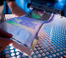
Organic solar cells can reduce the cost of solar power by using inexpensive organic polymers instead of the expensive crystalline silicon used in most solar cells. Moreover, polymers can be processed using low-cost equipment, such as inkjet printers or coating equipment used for manufacturing photographic film, which reduces both capital and operating costs compared with traditional solar cell manufacturing. [26]
Silicon thin-film solar cells on flexible substrates can significantly reduce the cost of large-area photovoltaic cells for several reasons: [27]
Inexpensive polymer substrates, such as polyethylene terephthalate (PET) or polycarbonate (PC), can help further reduce the cost of photovoltaic systems. Protomorphic solar cells have proven to be a promising concept for efficient, low-cost photovoltaic cells on cheap, flexible substrates for large-area production, as well as for small and mobile applications. [27]
One advantage of printed electronics is that various electrical and electronic components can be printed on top of one another, saving space and increasing reliability, and sometimes all of them are transparent. One set of inks must not damage another, and low-temperature annealing is essential if inexpensive flexible materials such as paper and plastic film are to be used. Many complex engineering and chemical technologies are involved here, among the leaders being iTi, Pixdro, Asahi Kasei, Merck & Co. | Merck, BASF, HC Starck, Hitachi Chemical, and Frontier Carbon Corporation. [28] Electronic devices based on organic compounds are now widely used, and many new products are under development. Sony reported the first full-color flexible plastic display with high video playback speed made entirely of organic materials; [29] [30] a television screen based on OLED materials; biodegradable electronics based on organic compounds and low-cost organic solar cells are also available.
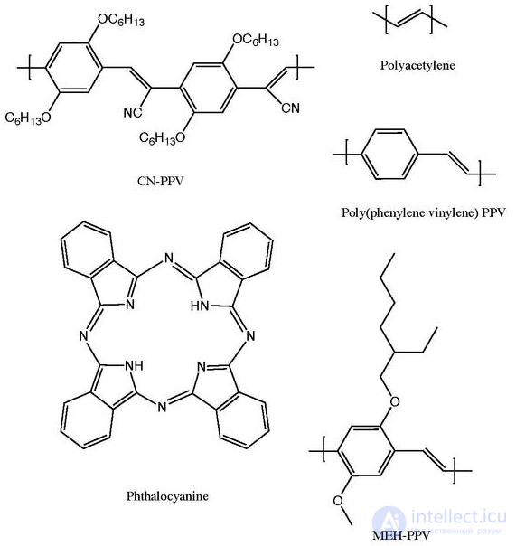
Five structures of organic photovoltaic materials
There are important differences between the processing of small-molecule organic semiconductors and semiconducting polymers. Small-molecule semiconductors are quite often insoluble and typically require deposition by vacuum sublimation. Soluble conjugated polymers, by contrast, are usually deposited as thin films. Devices based on conducting polymers can be fabricated using solution-processing methods. Both solution-processing methods and vacuum-based methods can produce amorphous and polycrystalline films with varying degrees of disorder. "Wet" coating techniques require the polymer to be dissolved in a volatile solvent, filtered, and applied to a substrate. Common examples of solvent-based coating methods include drop casting, spin coating, doctor blading, inkjet printing, and screen printing. Spin coating is a widely used technique for producing thin films over small areas. It can result in significant material loss. The doctor-blade method results in minimal material loss and was developed primarily for producing large-area thin films. Thermal deposition of small molecules in vacuum requires evaporating the molecules from a hot source. The molecules are then transported through the vacuum to the substrate. Condensation of these molecules on the substrate surface results in the formation of a thin film. In some cases, wet-coating methods can be applied to small molecules, depending on their solubility.
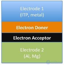
Compared with conventional inorganic solar cells, organic solar cells have the advantage of lower manufacturing cost. An organic photovoltaic cell is a device that uses organic electronics to convert light into electricity. Organic solar cells use organic photovoltaic materials — organic semiconducting diodes that convert light into electricity. The figure on the right shows the five most commonly used organic photovoltaic materials. Electrons in these organic molecules can be delocalized over a delocalized π orbital with a corresponding π* antibonding orbital. The energy difference between the π orbital, or highest occupied molecular orbital (HOMO), and the π* orbital, or lowest unoccupied molecular orbital (LUMO), is called the band gap of the organic photovoltaic material. The band gap typically falls in the range of 1–4 eV.
Differences in the band gap of organic photovoltaic materials lead to different chemical structures and forms of organic solar cells. Different solar cell architectures include single-layer organic photovoltaic cells, bilayer organic photovoltaic cells, and heterojunction photovoltaic cells. However, all three of these solar cell types share the approach of placing an organic electronic layer between two metal conductors, typically made of indium tin oxide. [34]
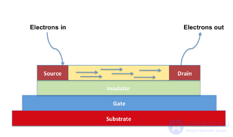
An organic field-effect transistor device consists of three main components: the source, the drain, and the gate. Typically, a field-effect transistor has two plates, with the source in contact with the drain and the gate acting as the conductive channel. Electrons move from the source to the drain, and the gate serves to control the movement of electrons from source to drain. Different types of field-effect transistors are designed based on carrier properties. The thin-film transistor (TFT), among others, is simple to fabricate. In a thin-film transistor, the source and drain are formed by depositing a thin semiconductor layer directly, followed by a thin insulating film between the semiconductor and the metal gate contact. Such a thin film is produced by thermal evaporation or simply by spin coating. In a TFT device, there is no carrier movement between source and drain. After a positive charge is applied, the accumulation of electrons at the interface causes the semiconductor to bend and ultimately lowers the conduction band relative to the semiconductor's Fermi level. Finally, a highly conductive channel forms at the interface.
Conducting polymers are lighter, more flexible, and cheaper than inorganic conductors. This makes them a desirable alternative in many applications. It also creates the potential for new applications that would be impossible using copper or silicon.
Organic electronics encompasses not only organic semiconductors but also organic dielectrics, conductors, and light emitters.
New applications include smart windows and electronic paper. Conducting polymers are expected to play an important role in the emerging science of molecular computing.

Comments