
Lecture
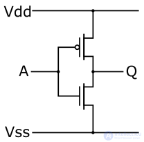
CMOS (complementary metal-oxide-semiconductor) is a set of semiconductor technologies for building integrated circuits and the corresponding circuit design approach. The vast majority of modern digital integrated circuits are CMOS.
In a more general sense, the term is MOS (metal-dielectric-semiconductor structure). CMOS technology uses insulated-gate field-effect transistors with channels of different conductivity types. A distinguishing feature of CMOS circuits compared to bipolar technologies (TTL, ECL, etc.) is very low power consumption in the static mode (in most cases it can be assumed that energy is consumed only during switching of logic states). A distinguishing feature of the CMOS structure compared to other MOS structures (NMOS, PMOS) is the presence of both n-channel and p-channel field-effect transistors located in the same area of the die. Because the distance between elements is smaller, CMOS circuits have higher speed and lower power consumption, but they are also characterized by a more complex manufacturing process and lower packing density on the die surface.
Discrete insulated-gate field-effect transistors (MOSFETs, metal-oxide-semiconductor field-effect transistors) are manufactured using a similar technology.
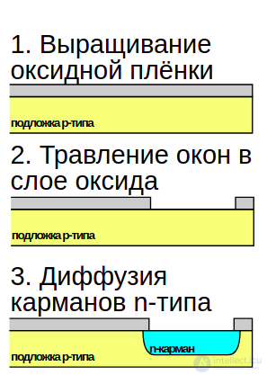
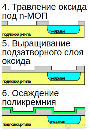
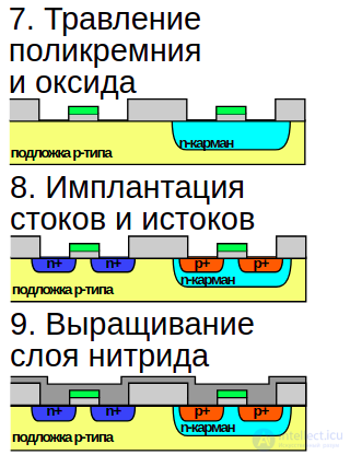
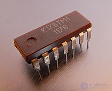
CMOS circuits were invented in 1963 by Frank Wanlass[en] at Fairchild Semiconductor, and the first CMOS chips were produced in 1968. For a long time CMOS was regarded as an energy-saving but slow alternative to TTL, so CMOS chips found use in electronic watches, calculators, and other battery-powered devices where power consumption was critical.
By 1990, as chip integration density increased, the problem of power dissipation in circuit elements became pressing. As a result, CMOS technology found itself in a favorable position. Over time, switching speeds and mounting densities were achieved that were unattainable with technologies based on bipolar transistors.
Early CMOS circuits were highly vulnerable to electrostatic discharge. Today this problem has largely been solved, but it is still recommended to take precautions against static charge buildup when handling CMOS chips.
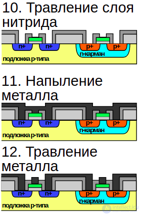
Aluminum was used for the gates in CMOS cells in the early stages. Later, with the advent of the so-called self-aligned process — which used the gate not only as a structural element but also simultaneously as a mask when forming the source and drain regions — polycrystalline silicon began to be used for the gate instead.
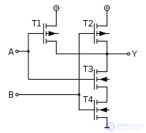
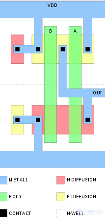
As an example, let us consider the circuit of a 2-input NAND gate built using CMOS technology.
The circuit contains no load resistors at all, so in the static state only leakage currents flow through the CMOS circuit via the turned-off transistors, and power consumption is very low. During switching, electrical energy is spent mainly on recharging the capacitances of the gates and interconnects, so the power consumed (and dissipated) is proportional to the switching frequency (for example, the clock frequency of a processor).
The NAND chip configuration diagram shows that it uses two dual-gate field-effect transistors with different channel conductivity types. The upper dual-gate field-effect transistor produces a high level at the output of the logic gate if either of its gates is at a low level, while the lower dual-gate field-effect transistor produces a high level at the output of the logic gate if both of its gates are at a high level.
It should be noted that, since switching of the n-channel and p-channel transistors takes a finite amount of time, both transistor types can briefly be turned on simultaneously, producing a pulsed through-current between the supply rails. This leads to increased power consumption.
Because the gates of MOS transistors have very high input resistance, an electrostatic discharge can cause gate breakdown and chip failure. To protect against static electricity, each pin of a CMOS chip is fitted with a protective circuit that includes low-breakdown-voltage diodes connecting each input to the supply rails.
"CMOS" refers both to a specific style of digital circuit design and to a family of processes used to implement that circuitry on integrated circuits (chips). CMOS circuits dissipate less energy than logic families with resistive loads. As this advantage grew and became increasingly important, CMOS processes and variants came to dominate, so that the vast majority of modern integrated circuit manufacturing today is based on CMOS processes. CMOS logic consumes more than 7 times less energy than NMOS logic, and roughly 100,000 times less energy than bipolar transistor-transistor logic (TTL).
CMOS circuits use a combination of p-type and n-type metal-oxide-semiconductor field-effect transistors (MOSFETs) to implement logic gates and other digital circuits. Although CMOS logic can be implemented using discrete devices for demonstration purposes, commercial CMOS products are integrated circuits consisting of billions of transistors of both types on a rectangular piece of silicon with an area of 10 to 400 mm2.
CMOS always uses all MOSFETs in enhancement mode (in other words, zero gate-source voltage turns the transistor off).
For more flexible use, a number of manufacturers also offer special families in which each IC contains just a single logic element in a 5- or 6-pin package, which can be useful for designs with a small number of different elements and a minimal board size (for example: 74LVC1G00GW from NXP; SOT353-1 Single 2-Input Positive-AND Gate)

Comments