
Lecture
Memristor ( /mɛmˈrɪstər/ , a portmanteau of "memory resistor" ) is a nonlinear two-terminal electrical component that relates electric charge and magnetic flux linkage. It was described and named in 1971 by Leon Chua, completing the theoretical quartet of fundamental electrical components, which also includes the resistor, capacitor, and inductor. No physical memristor component has yet been demonstrated.
Chua and Kang later generalized this concept to memristive systems . Such a system contains a circuit made of several ordinary components that mimics the key properties of the ideal memristor component and is also commonly referred to as a memristor. Several such memristive systems have been developed, most notably ReRAM .
The identification of genuine memristive properties in both theoretical and practical devices remains a subject of controversy.
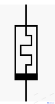 Electronic symbol
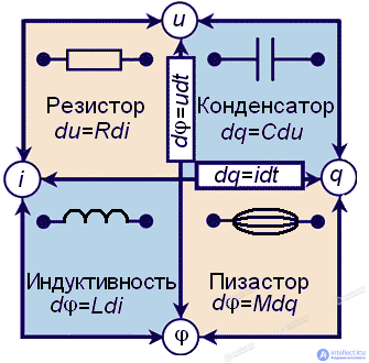
Conceptual symmetries of the resistor, capacitor, inductor, and memristor.
In his 1971 paper, Chua identified a theoretical symmetry between the nonlinear resistor (voltage vs. current), the nonlinear capacitor (voltage vs. charge), and the nonlinear inductor (magnetic flux linkage vs. current). From this symmetry he derived the characteristics of a fourth fundamental nonlinear circuit element relating magnetic flux and charge, which he named the memristor. Unlike a linear (or nonlinear) resistor, a memristor has a dynamic relationship between current and voltage that includes a memory of past voltages or currents. Other scientists had proposed resistors with dynamic memory, such as Bernard Widrow's "memistor," but Chua introduced mathematical generality.
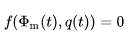
The memristor was originally defined in terms of a nonlinear functional relationship between magnetic flux linkage Φm ( t ) and the amount of electric charge that has flowed, q ( t ):
Magnetic flux linkage, Φm, is generalized here from the characteristic circuit behavior of the inductor. It does not represent a magnetic field in this context. Its physical meaning is discussed below. The symbol Φm can be thought of as the time integral of voltage.
In the relationship between Φm and q, the derivative of one with respect to the other depends on the value of one or the other, and so each memristor is characterized by its memristance function, describing the charge-dependent rate of change of flux with charge,
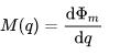
Substituting flux as the time integral of voltage and charge as the time integral of current, more convenient forms are:
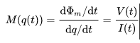
To relate the memristor to the resistor, capacitor, and inductor, it is useful to isolate the term M ( q ), which characterizes the device, and write it as a differential equation.
| Device | Characteristic property (units) | Differential equation |
|---|---|---|
| Resistor (R) | Resistance ( V/A , or ohm , Ω) | R = dV / dI |
| Capacitor (C) | Capacitance ( C/V , or farad ) | C = dq / dV |
| Inductor (L) | Inductance ( Wb/A , or henry ) | L = dΦm / dI |
| Memristor (M) | Memristance ( Wb/C , or ohm) | M = dΦm / dq |
The table above covers all the meaningful differential relationships among I , Q , Φm , and V . No device can relate dI to dQ , or dΦm to dV , because I is the derivative of Q and Φm is the integral of V .
From this it can be concluded that memristance is charge-dependent resistance. If M ( q ( t )) is constant, we obtain Ohm's law R ( t ) = V ( t ) / I ( t ). However, if M ( q ( t )) is nontrivial, the equation is not equivalent, since q ( t ) and M ( q ( t )) may vary with time. Solving for voltage as a function of time yields
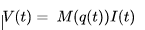
This equation shows that memristance defines a linear relationship between current and voltage as long as M does not depend on charge. A nonzero current implies a time-varying charge. Alternating current, however, can reveal a linear relationship in the circuit's operation by producing a measurable voltage without net charge movement, as long as the maximum change in q does not cause a significant change in M .
Moreover, a memristor is static if no current is applied. If I ( t ) = 0, we find V ( t ) = 0 and M ( t ) is constant. This is the essence of the memory effect.
Similarly, we can define  as a special case.
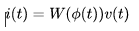
Power consumption is characteristically reminiscent of that of a resistor, I 2R .

As long as M ( q ( t )) changes little, for example under alternating current, the memristor will behave as a constant resistor. However, if M ( q ( t )) increases rapidly, the current and power consumption will quickly cease.
M ( q ) is physically constrained to be positive for all values of q (assuming the device is passive and does not become superconducting at some q ). A negative value would mean it would continuously supply energy when operated with alternating current.
To understand the nature of the memristor function, it is useful to have some knowledge of fundamental theoretical circuits, starting with the concept of device modeling.
Engineers and scientists rarely analyze a physical system in its original form. Instead, they build a model that approximates the system's behavior. By analyzing the model's behavior, they hope to predict the behavior of the real system. The main reason for building models is that physical systems are usually too complex to be subjected to practical analysis.
In the 20th century, work was done on devices in which researchers did not recognize memristive characteristics. This has given rise to the suggestion that such devices should be recognized as memristors. Pershin and Di Ventra proposed a test that could help resolve some long-standing disputes about whether the ideal memristor actually exists or is a purely mathematical concept.
The remainder of this article mainly deals with memristors related to ReRAM devices, since most of the work since 2008 has been focused in this area.
Dr. Paul Penfield, in a 1974 MIT technical report, mentions the memristor in connection with Josephson junctions. This was an early use of the word "memristor" in the context of circuit design.
One of the terms in the flux through a Josephson junction has the form:
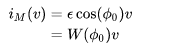
where  is a constant based on the physical superconducting materials,
  is the voltage across the junction, and
  is the current through the junction.
In the late 20th century, research was conducted on this phase-dependent conductance in Josephson junctions. [10] A more comprehensive approach to extracting this phase-dependent conductance appeared with the original paper by Peotta and DiVentra in 2014. [11]
Due to the practical difficulty of studying an ideal memristor, we will discuss other electrical devices that can be modeled using memristors. For a mathematical description of memristive devices (systems), see the section "Theory" .
A gas discharge tube can be modeled as a memory device with resistance being a function of the number of conduction electrons  ,
,
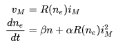
 is the voltage across the discharge tube, is the current flowing through it, and is the number of conduction electrons. A simple memristance function
 , with
  and
and  being parameters depending on the tube's dimensions and gas fill. The experimental identifier of memristive behavior is a "pinched hysteresis loop" in the
  plane. For an experiment demonstrating such a characteristic for an ordinary gas discharge tube, see "Physical Memristor Lissajous Figure" (YouTube) . The video also shows how to understand deviations in the pinched hysteresis characteristics of physical memristors. [12] [13]
Thermistors can be modeled as memory devices. [13]
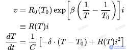
 is a material constant,
  is the absolute temperature of the thermistor body,
  is the ambient temperature (both temperatures in kelvins),
  denotes the cold resistance at
  ,
,  is the thermal capacity, and
  is the dissipation constant of the thermistor.
A fundamental phenomenon that is barely studied is memristive behavior in pn junctions. [14] The memristor plays a key role in simulating the effect of charge accumulation at the base of a diode, and is also responsible for the phenomenon of conductivity modulation (which is very important during forward-direction transients).
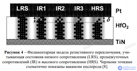
The availability of experimental data confirming the local nature of resistive switching has, in the scientific community, in addition to the mechanism of valence-state change of the dielectric material across the entire structure area (Figure 4), stimulated the development of a switching model based on the formation of local conducting channels (filaments) Error! Reference source not found.. Thus, taking into account the importance of oxygen vacancy generation for resistive switching processes, a resistive switching model was proposed that explains, among other things, the possibility of obtaining an entire set of intermediate resistances of an MIM structure depending on the voltage applied to it (the memristive effect itself) (Figure 4).
In 2008, a team at HP Labs claimed to have found Chua's missing memristor based on an analysis of a thin titanium dioxide film, thus linking the operation of ReRAM devices to the memristor concept. According to HP Labs, the memristor works as follows: the electrical resistance of a memristor is not constant, but depends on the history of the current that has previously flowed through the device — that is, its current resistance depends on how much electric charge has flowed in which direction through it in the past; the device remembers its history — the so-called nonvolatility property . [15] When power is turned off, the memristor remembers its most recent resistance until it is turned on again. [16] [17]
The HP result was published in the scientific journal Nature . [16] [18] Following this claim, Leon Chua argued that the definition of the memristor could be generalized to cover all forms of two-terminal nonvolatile memory devices based on resistance-switching effects. [15] Chua also argued that the memristor is the oldest known circuit element, with its effects predating the resistor, capacitor, and inductor. [19]
However, there are serious doubts as to whether a true memristor can actually exist in physical reality. [20] [21] [22] [23] [24] In addition, some experimental data contradict Chua's generalization, since a non-passive "nanobattery" effect is observed in resistance-switching memory. [25] Pershin and Di Ventra proposed a simple test to analyze whether such an ideal or universal memristor actually exists or is a purely mathematical concept. So far, no experimental resistance-switching device (ReRAM) appears to have passed the test. [26]
These devices are intended for application in nanoelectronic memory, computer logic, and neuromorphic/neuromemristive computing architecture. [27] [28] [29] In 2013, Hewlett-Packard's CTO Martin Fink suggested that memristor memory could become commercially available as early as 2018. [30] In March 2012, a group of researchers from HRL Laboratories and the University of Michigan announced the first functioning memristor array built on a CMOS chip. [31]
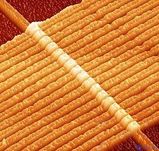
An array of 17 specially engineered oxygen-depleted titanium dioxide-based memristors, created in HP's laboratory, imaged with an atomic force microscope. The wires are approximately 50 nm, or 150 atoms, wide. [32] Electric current through the memristors shifts oxygen vacancies, causing a gradual and permanent change in electrical resistance. [33]
According to the original 1971 definition, the memristor was the fourth fundamental circuit element, forming a nonlinear relationship between electric charge and magnetic flux linkage. In 2011, Chua advocated for a broader definition that included all two-terminal nonvolatile memory devices based on resistance switching. [15] Williams argued that MRAM, phase-change memory, and ReRAM were all memristor technologies. [34] Some researchers have argued that biological structures such as blood [35] and skin [36] [37] meet the definition. Others have argued that the memory device being developed by HP Labs and other forms of ReRAM were not memristors but rather part of a broader class of variable-resistance systems [38], and that the broader definition of the memristor is a scientifically unjustified land grab that favored HP's memristor patents. [39]
In 2011, Meuffels and Schroeder noted that one of the early memristor papers contained an erroneous assumption regarding ionic conductivity. [40] In 2012, Meuffels and Soni discussed some fundamental issues and problems in the implementation of memristors. [20] They pointed out flaws in the electrochemical modeling presented in the Nature paper "The missing memristor found" [16], since the influence of concentration polarization effects on the behavior of metal–TiO2−x–metal structures under voltage or current stress was not taken into account. This criticism was referenced by Valov et al. [25] in 2013.
In a peculiar thought experiment, Meuffels and Soni [20] additionally identified serious inconsistencies: if a current-controlled memristor with the so-called nonvolatility property [15] existed in physical reality, its behavior would violate Landauer's principle regarding the minimum amount of energy required to change the "information" states of a system. This criticism was ultimately accepted by Di Ventra and Pershin [21] in 2013.
In this context, Meuffels and Soni [20] pointed out a fundamental thermodynamic principle: nonvolatile information storage requires the existence of free-energy barriers that separate the different internal memory states of a system from one another; otherwise one would encounter an "indifferent" situation, and the system would randomly fluctuate from one memory state to another under the influence of thermal fluctuations alone. In the absence of protection from thermal fluctuations, internal memory states exhibit some diffusive dynamics that causes state degradation. [21] Therefore, free-energy barriers must be sufficiently high to ensure a low probability of a bit error during a bit operation. [41] Consequently, there is always a lower limit on the energy required — depending on the required bit-error probability — to deliberately change a bit value in any memory device. [41] [42]
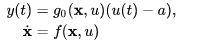
In the general concept of a memristive system, the governing equations are (see Theory ):
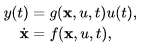
where u ( t ) is the input signal and y ( t ) is the output signal. The vector x represents a set of n state variables describing the various internal memory states of the device. ẋ is the time-dependent rate of change of the state vector x with time.
When one wants to go beyond simple curve fitting and aim for real physical modeling of nonvolatile memory elements, such as resistive random-access memory devices, one must adhere to the aforementioned physical correlations. To test the adequacy of the proposed model and the resulting state equations, the input signal u ( t ) can be superimposed with a stochastic term ξ ( t ) that accounts for the presence of unavoidable thermal fluctuations. The dynamic state equation, in its general form, finally looks as follows:

where ξ ( t ) is, for example, white Gaussian current or voltage noise. Based on analytical or numerical analysis of the time-dependent response of the system to noise, one can decide on the physical validity of the modeling approach — for example, whether the system will be able to retain its memory states when power is switched off.
Such an analysis was carried out by Di Ventra and Pershin [21] with respect to a true current-controlled memristor. Since the proposed dynamic state equation does not provide a physical mechanism allowing such a memristor to cope with unavoidable thermal fluctuations, a current-controlled memristor will, over time, randomly change its state under the influence of current noise. [21] [43] Di Ventra and Pershin [21] thus concluded that memristors whose resistance (memory) states depend solely on the history of current or voltage will be unable to protect their memory states from the unavoidable Johnson–Nyquist noise and will continuously suffer information loss, the so-called "stochastic catastrophe." Thus, a current-controlled memristor cannot exist as a physical device in physical reality.
The above thermodynamic principle further implies that the operation of two-terminal nonvolatile memory devices (such as "resistive switching" memory devices (ReRAM)) cannot be linked to the concept of the memristor — that is, such devices by themselves cannot remember their history of current or voltage. Transitions between different internal memory or resistance states are probabilistic in nature. The probability of a transition from state { i } to state { j } depends on the height of the free-energy barrier between the two states. Thus, the transition probability can be influenced by appropriately driving the memory device — that is, by "lowering" the free-energy barrier for the transition { i } → { j } via, for example, an external stimulus.
A "resistance switching" event can simply be forced by setting the external bias to a value above a certain threshold. This is the trivial case, i.e., the free-energy barrier for the transition { i } → { j } is reduced to zero. In the case of applying biases below the threshold value, there is still a finite probability that the device will switch over time (caused by random thermal fluctuations), but — since one is dealing with probabilistic processes — it is impossible to predict when the switching event will occur. This is the fundamental reason for the stochastic nature of all observed resistance switching (ReRAM) processes. If the free-energy barriers are not sufficiently high, the memory device may even switch without any action being taken.
When a two-terminal nonvolatile memory device is found to be in a particular resistance state { j }, there is therefore no physical one-to-one correspondence between its current state and its prior voltage history. Thus, the switching behavior of individual nonvolatile memory devices cannot be described within the mathematical framework proposed for memristor/memristive systems.
An additional thermodynamic curiosity follows from the definition that memristors/memristive devices must energetically behave as resistors. The instantaneous electrical power delivered to such a device is entirely dissipated as Joule heat to the environment, so no additional energy remains in the system after it has been transitioned from one resistance state xi to another xj . Thus, the internal energy of a memristor device in state xi , U ( V , T , xi ), would be the same as in state xj , U ( V , T , xj ), even though these different states would produce different device resistances, which itself must be caused by physical changes in the device's material.
Other researchers have noted that memristor models based on the assumption of linear ion drift fail to account for the asymmetry between set time (switching from high to low resistance) and reset time (switching from low to high resistance) and do not provide ion-mobility values consistent with experimental data. To compensate for this shortcoming, nonlinear ion-drift models have been proposed. [44]
In a 2014 paper, ReRAM researchers concluded that the initial/basic memristor modeling equations of Strukov (HP) do not reflect the real physics of the device, while later (physics-based) models, such as Pickett's model or Menzel's ECM model (Menzel being a co-author of the paper), have adequate predictive power but are computationally prohibitive. Since 2014, the search for a model that balances these concerns has continued; the paper discusses the Chang and Jakopcic models as potentially good compromises. [45]
Martin Reynolds, an electrical engineering analyst at Gartner's research division, noted that while HP somewhat clumsily calls its device a memristor, critics pedantically say it is not a memristor. [46]
In the paper "The Missing Memristor Has Not Been Found," published in Scientific Reports in 2015 by Vongehr and Meng [23], it was shown that a true memristor, as defined in 1971, is impossible without the use of magnetic induction. This was illustrated by constructing a mechanical analog of the memristor and then analytically showing that a mechanical memristor cannot be built without using inertial mass. Since it is well known that the mechanical equivalent of an electrical inductor is mass, this proves that memristors are impossible without the use of magnetic induction. Thus, it can be argued that variable-resistance devices such as ReRAM and conceptual memristors may have no equivalent at all. [23] [47]
Chua proposed conducting experimental tests to determine whether a device can properly be classified as a memristor:
According to Chua [48] [49], all resistive switching memory devices, including ReRAM, MRAM, and phase-change memory, satisfy these criteria and are memristors. However, a lack of data for Lissajous curves across a range of initial conditions or a range of frequencies makes it difficult to evaluate this claim.
Experimental data show that redox-based resistance memory (ReRAM) includes a nanobattery effect that contradicts Chua's memristor model. This indicates that memristor theory must be extended or corrected to provide an accurate model of ReRAM. [25]
In 2008, researchers at HP Labs presented a model for the memristance function based on thin titanium dioxide films. [16] For  , the memristance function was defined as

where ROFF represents the high-resistance state, RON represents the low-resistance state, μv represents the mobility of dopants in the thin film, and D represents the film thickness. The HP Labs group noted that "window functions" are necessary to compensate for discrepancies between experimental measurements and their memristor model due to nonlinear ion drift and boundary effects.
For some memristors, an applied current or voltage causes a substantial change in resistance. Such devices can be characterized as switches by examining the time and energy that must be expended to achieve the desired change in resistance. This assumes that the applied voltage remains constant. Solving for the energy dissipated during a single switching event shows that for a memristor to transition from Ron to Roff during time Ton to Toff , the charge must change by ∆q = Qon − Qoff .

Substituting V = I ( q ) M ( q ), and then ∫dq/V = ∆Q/V for constant V, gives the final expression. This power characteristic is fundamentally different from that of a metal-oxide-semiconductor capacitor-based transistor. Unlike a transistor, the final state of the memristor in terms of charge does not depend on the bias voltage.
The type of memristor described by Williams stops being ideal after switching across the full resistance range, creating hysteresis, also called a "hard-switching regime." [16] Another type of switch would have a cyclic M ( Q ) so that every off-to-on event would be followed by an on-to-off event at constant bias. Such a device would behave as a memristor under any conditions but would be less practical.
In the more general concept of an nth-order memristive system, the governing equations are
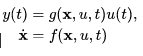
where u ( t ) is the input signal, y ( t ) is the output signal, the vector x represents a set of n state variables describing the device, and g and f are continuous functions . For a current-controlled memristive system, the signal u ( t ) represents the current signal i ( t ), and the signal y ( t ) represents the voltage signal v ( t ). For a voltage-controlled memristive system, the signal u ( t ) represents the voltage signal v ( t ), and the signal y ( t ) represents the current signal i ( t ).
The pure memristor is a special case of these equations, namely when x depends only on charge ( x = q ) and since charge is related to current through the time derivative dq/dt = i ( t ). Thus, for pure memristors, f (i.e., the rate of change of state) must be equal or proportional to the current i ( t ).
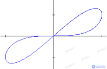
Example of a pinched hysteresis curve, V vs. I
One of the resulting properties of memristors and memristive systems is the presence of a pinched hysteresis effect. [50] For a current-controlled memristive system, the input u ( t ) represents the current i ( t ), the output y ( t ) represents the voltage v ( t ), and the slope of the curve represents electrical resistance. Changes in the slope of the pinched hysteresis curves demonstrate switching between different resistance states, a phenomenon central to ReRAM and other forms of two-terminal resistance memory. At high frequencies, memristive theory predicts that the pinched hysteresis effect will degenerate, resulting in a straight-line representation of a linear resistor. It has been shown that memristors cannot describe certain types of non-crossing pinched hysteresis curves (designated as type II). [51]
Some researchers have raised questions about the scientific legitimacy of HP's memristor models in explaining ReRAM behavior [38] [39] and have proposed extended memristive models to address the identified shortcomings. [25]
In one example [52], an attempt is made to extend the framework of memristive systems by including dynamical systems involving higher-order derivatives of the input signal u ( t ) in the form of a series expansion.

where m is a positive integer, u ( t ) is the input signal, y ( t ) is the output signal, the vector x represents a set of n state variables describing the device, and the functions g and f are continuous functions . This equation produces the same zero-crossing hysteresis curves as memristive systems, but with a different frequency response than that predicted by memristive systems.
In another example, it is proposed to include an offset value a to account for the observed nanobattery effect, which disrupts the predicted zero-crossing pinched hysteresis effect. [25]
Interest in the memristor was revived when, in 2007, R. Stanley Williams of Hewlett Packard reported an experimental solid-state version. [53] [54] [55] This paper was the first to demonstrate that a solid-state device could have the characteristics of a memristor based on the behavior of nanoscale thin films. The device does not use magnetic flux, as proposed by the theoretical memristor, and does not store charge like a capacitor, but instead achieves a resistance that depends on the history of current.
Although not mentioned in HP's original reports on their TiO2 memristor, the resistance-switching characteristics of titanium dioxide were originally described in the 1960s. [56]
The HP device consists of a thin (50 nm) film of titanium dioxide between two 5 nm thick electrodes: one titanium, the other platinum. Initially, the titanium dioxide film has two layers, one of which has a slight depletion of oxygen atoms. Oxygen vacancies act as charge carriers, which means the depleted layer has much lower resistance than the non-depleted layer. When an electric field is applied, the oxygen vacancies drift (see fast ion conductor ), shifting the boundary between the high- and low-resistance layers. Thus, the resistance of the film as a whole depends on how much charge has passed through it in a given direction, which is reversible when the direction of the current is changed. [16] Because the HP device exhibits fast ionic conductivity at the nanoscale, it is considered a nanoionic device. [57]
Memristance is displayed only when both the doped layer and the depleted layer contribute to the resistance. When enough charge has passed through the memristor that the ions can no longer move, the device enters hysteresis. It stops integrating q = ∫I dt , but retains q at its upper bound and fixes M , thereby acting as a constant resistor until the current changes direction.
The application of thin-film oxide memory has been an area of active research for some time. In 2000, IBM published a paper on structures similar to those described by Williams. [58] Samsung holds a US patent on oxygen-vacancy switches similar to the one described by Williams. [59] Williams also has a US patent application related to the memristor design. [60]
In April 2010, HP Labs announced that they had practical memristors operating with a switching time of 1 ns (~1 GHz) and dimensions of 3 nm by 3 nm [61], foreshadowing the future of this technology. [62] At such densities, it could easily compete with current flash memory technology below 25 nm .
In 2004, Krieger and Spitzer described dynamic doping of polymeric and inorganic dielectric materials, which improved the switching and retention characteristics needed to create functioning nonvolatile memory cells. [63] They used a passive layer between the electrode and the active thin films, which enhanced ion extraction from the electrode. A fast ion conductor can be used as this passive layer, allowing the ion-extraction field to be significantly reduced.
In July 2008, Erokhin and Fontana claimed to have developed a polymer memristor before the titanium dioxide memristor was recently announced. [64]
In 2010, Alibart, Gamrat, Vuillaume et al. [65] presented a new hybrid organic/nanoparticle device (NOMFET: nanoparticle organic memory field-effect transistor) that behaves as a memristor [66] and demonstrates the essential behavior of a biological synapse spike. This device, also called a synapstor (synapse transistor), was used to demonstrate a neuro-inspired circuit (an associative memory demonstrating Pavlovian learning) [67]
In 2012, Crupi, Pradhan, and Tozer described a conceptual design for creating neural synaptic memory circuits using organic ion-based memristors. [68] The synapse circuit demonstrated long-term potentiation for learning as well as forgetting based on inactivity. Using a grid of circuits, a light pattern was stored and later recalled. This mimics the behavior of V1 neurons in the primary visual cortex, which act as spatiotemporal filters that process visual signals such as edges and moving lines.
In 2014, Bessonov et al. reported a flexible memristive device containing a MoO x /MoS 2 heterostructure sandwiched between silver electrodes on a plastic foil. [69] The fabrication method is based entirely on printing and solution-processing techniques using two-dimensional layered transition metal dichalcogenides (TMDs). The memristors are mechanically flexible, optically transparent, and inexpensive to produce. It was found that the memristive behavior of the switches is accompanied by a pronounced memcapacitive effect. The high switching efficiency, demonstrated synaptic plasticity, and resistance to mechanical deformation promise to mimic attractive characteristics of biological neural systems in emerging computing technologies.
An atomristor is defined as an electrical device exhibiting memristive behavior in atomically thin nanomaterials or atomic sheets. In 2018, Ge, Wu, et al. [70] first reported a universal memristive effect in single-layer atomic sheets of TMDs (MX 2 , M = Mo, W; and X = S, Se) based on a vertical metal-insulator-metal (MIM) device structure. These atomristors enable forming-free switching as well as unipolar and bipolar operation. Switching behavior is observed in both single-crystal and polycrystalline films with various metal electrodes (gold, silver, and graphene). Atomically thin TMD sheets are prepared via CVD/MOCVD, enabling low-cost fabrication. Subsequently, taking advantage of the low "on" resistance and large "on/off" ratio, a high-performance zero-power RF switch based on MoS 2 atomristors was demonstrated, pointing to a new application for memristors. [71]
The ferroelectric memristor [72] is based on a thin ferroelectric barrier placed between two metal electrodes. Switching the polarization of the ferroelectric material by applying a positive or negative voltage to the junction can produce a resistance change of two orders of magnitude: R OFF ≫ R ON (an effect called tunneling electroresistance). In general, the polarization does not switch abruptly. The reversal occurs gradually through the nucleation and growth of ferroelectric domains with opposite polarization. During this process the resistance is neither R ON nor R OFF, but somewhere in between. As the voltage is cycled, the ferroelectric domain configuration evolves, allowing fine tuning of the resistance value. The main advantages of the ferroelectric memristor are that the dynamics of the ferroelectric domains can be adjusted, offering a way to engineer the memristor's response, and that the resistance variations are caused by purely electronic phenomena, which improves device reliability since no deep structural change of the material occurs.
In 2013, Ageev, Blinov, et al. [73] reported observing a memristor effect in a structure based on vertically aligned carbon nanotubes, studying bundles of CNTs with a scanning tunneling microscope.
It was later found [74] that memristive switching of a CNT is observed when the nanotube has a nonuniform elastic strain ΔL ≠ 0. It was shown that the memristive switching mechanism of a strained CNT is based on the formation and subsequent redistribution of nonuniform elastic strain and the piezoelectric field Edef in the nanotube under the influence of an external electric field E(x, t).
Spintronic memristor
Researchers from Seagate Technology, Chen and Wang, described three examples of possible magnetic memristors. [75] In one device, resistance arises when the spin of electrons in one section of the device points in a direction different from that in another section, creating a "domain wall," a boundary between the two sections. Electrons entering the device have a certain spin, which alters the magnetization state of the device. The change in magnetization, in turn, moves the domain wall and changes the resistance. The significance of the work led to an interview with IEEE Spectrum. [76] The first experimental demonstration of a spintronic memristor based on domain-wall motion driven by spin currents in a magnetic tunnel junction was presented in 2011. [77]
Memristance in a magnetic tunnel junction
It has been proposed that a magnetic tunnel junction acts as a memristor through several potentially complementary mechanisms, both extrinsic (redox reactions, charge trapping/detrapping, and electromigration within the barrier) and intrinsic (spin-transfer torque).
Extrinsic mechanism
Building on studies carried out between 1999 and 2003, Bowen et al. published in 2006 experiments on a magnetic tunnel junction (MTJ) exhibiting bistable spin-dependent states [78] (resistive switching). The MTJ consists of an SrTiO3 (STO) tunnel barrier separating a half-metallic oxide LSMO electrode and a ferromagnetic metallic CoCr electrode. The usual two resistance states of the MTJ device, characterized by parallel or antiparallel alignment of the electrode magnetizations, are altered by applying an electric field. When the electric field is applied from the CoCr to the LSMO electrode, the tunneling magnetoresistance (TMR) ratio is positive. When the direction of the electric field is reversed, the TMR is negative. In both cases, large TMR amplitudes, on the order of 30%, are observed. Since a fully spin-polarized current flows from the half-metallic LSMO electrode within the Julliere model, this sign change suggests a sign change in the effective spin polarization of the STO/CoCr interface. The cause of this multilayer effect is the observed migration of Cr into the barrier and its degree of oxidation. The sign change of the TMR can be caused by modifications of the density of states at the STO/CoCr interface, as well as by changes in the tunneling landscape at the STO/CoCr boundary caused by CrOx redox reactions.
Reports of memristive switching based on MgO in MgO-based MTJs have appeared starting in 2008 [79] and 2009. [80] While the drift of oxygen vacancies in the insulating MgO layer was proposed to explain the observed memristive effects, [80] another explanation could be charge trapping/detrapping at localized states of oxygen vacancies [81] and its effect [82] on spintronics. This underscores the importance of understanding the role of oxygen vacancies in the memory operation of devices employing complex oxides with intrinsic properties such as ferroelectricity [83] or multiferroicity. [84]
Intrinsic mechanism
The magnetization state of an MTJ can be controlled by spin-transfer torque and thus, through this intrinsic physical mechanism, can exhibit memristive behavior. This torque is induced by the current flowing through the junction and provides an efficient way to achieve MRAM. However, the duration of the current flowing through the junction determines the magnitude of current required, i.e., charge is the key variable. [85]
The combination of intrinsic (spin-transfer torque) and extrinsic (resistive switching) mechanisms naturally leads to a second-order memristive system described by the state vector x = (x1, x2), where x1 describes the magnetic state of the electrodes and x2 denotes the resistive state of the MgO barrier. In this case, the change in x1 is governed by the current (the torque is due to high current density), whereas the change in x2 is governed by the voltage (the drift of oxygen vacancies is driven by strong electric fields). The presence of both effects in a memristive magnetic tunnel junction has led to the idea of a nanoscale synapse-neuron system. [86]
Spin memristive system
A fundamentally different mechanism of memristive behavior was proposed by Pershin [87] and Di Ventra. [88] [89] The authors show that certain types of semiconductor spintronic structures belong to the broad class of memristive systems, as defined by Chua and Kang. The mechanism of memristive behavior in such structures is based entirely on the electron spin degree of freedom, which provides more convenient control than ionic transport in nanostructures. When an external control parameter (such as voltage) is changed, the adjustment of the electron spin polarization is delayed due to diffusion and relaxation processes that cause hysteresis. This result was expected from studies of spin extraction at semiconductor/ferromagnet interfaces [90], but had not been described in terms of memristive behavior. In the short term, these structures behave almost like an ideal memristor. This result broadens the possible range of applications of semiconductor spintronics and represents a step forward toward future practical applications.
In 2017, Dr. Chris Campbell officially introduced the self-directed channel (SDC) memristor. [91] The SDC device is the first memory device commercially available to researchers, students, and electronics hobbyists worldwide. [92] The SDC device works immediately after fabrication. In the active Ge 2 Se 3 layer, homopolar Ge-Ge bonds are found and switching occurs. Three layers, consisting of Ge 2 Se 3/Ag/Ge 2 Se 3 directly beneath the top tungsten electrode, intermix during deposition and jointly form the silver source layer. An SnSe layer sits between these two layers, ensuring that the silver source layer is not in direct contact with the active layer. Because silver does not migrate into the active layer at high temperatures, and the active layer maintains a high glass transition temperature of around 350 °C (662 °F), the device has significantly higher processing and operating temperatures, at 250 °C (482 °F) and at least 150 °C (302 °F) respectively. These processing and operating temperatures are higher than those of most types of ion-conducting chalcogenide devices, including S-based glasses (such as GeS), which must be photodoped or thermally annealed. These factors allow the SDC device to operate over a wide temperature range.
Memristors remain a laboratory curiosity, as they are not yet mature enough to reach any commercial applications. Despite the lack of mass availability, according to Allied Market Research the memristor market was worth $3.2 million in 2015 and is projected to reach $79.0 million by 2022. [93]
A potential application of memristors is in analog memory for superconducting quantum computers. [11]
Memristors could potentially be turned into nonvolatile solid-state memory that could provide greater data density than hard drives with access times comparable to DRAM, replacing both components. [33] HP built a prototype crossbar latch memory device capable of holding 100 gigabits per square centimeter, [94] and proposed a scalable 3D design (comprising 1000 layers, or 1 petabit per cm 3 ). [95] In May 2008, HP reported that its device currently achieves about one-tenth the speed of DRAM. [96] The device's resistance would be read out with alternating current, so that the stored value would not be affected. [97] In May 2012, it was reported that access time had been improved to 90 nanoseconds, almost a hundred times faster than contemporary flash memory. At the same time, power consumption was only one percent of that of flash memory. [98]
Memristor patents include applications in programmable logic, [99] signal processing, [100] physical neural networks, [101] control systems, [102] reconfigurable computing, [103] brain-computer interfaces, [104] and RFID. [105] Memory devices are potentially used for stateful logic implication, which would allow CMOS-based logic computation to be replaced. Several early works have been reported in this direction. [106] [107]
In 2009, a simple electronic circuit [108] consisting of an LC network and a memristor was used to model experiments on the adaptive behavior of unicellular organisms. [109] It was shown that under the influence of a sequence of periodic pulses, the circuit remembers and anticipates the next pulse, similar to the behavior of the slime mold Physarum polycephalum, in which the viscosity of channels in the cytoplasm responds to periodic changes in the environment. [109] Applications of such circuits could include, for example, pattern recognition. DARPA's SyNAPSE project, funded by HP Labs in collaboration with Boston University's Neuromorphics Lab, is developing neuromorphic architectures that could be based on memristive systems. In 2010, Versace and Chandler described the MoNETA (Modular Neural Exploring Traveling Agent) model. [110] MoNETA is the first large-scale neural network model implementing whole-brain circuits to power a virtual and robotic agent using memory hardware. [111] The application of the memristor crossbar structure in building an analog soft-computing system was demonstrated by Merrikh-Bayat and Shouraki. [112] In 2011, they showed [113] how memristor crossbars can be combined with fuzzy logic to create an analog memristive neuro-fuzzy computing system with fuzzy input and output terminals. Learning is based on the creation of fuzzy relations founded on Hebbian learning rules.
In 2013, Leon Chua published a tutorial paper highlighting the wide range of complex phenomena and applications spanning memristors, and ways they can be used as nonvolatile analog memory and can mimic classical phenomena of habituation and learning. [114]
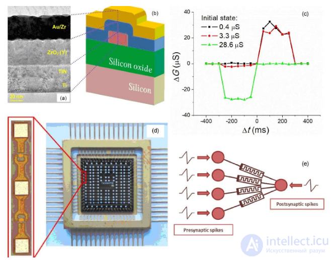
Hardware implementation of a spiking neural network based on memristors. The key elements of such a network, along with spiking neurons, are artificial synaptic connections that can change the strength (weight) of the connection between neurons during learning. Memristive devices based on "metal-oxide-metal" nanostructures, developed at the NIFTI of Lobachevsky University (UNN), are suitable for this purpose; however, using them in specific spiking neural network architectures being developed at the Kurchatov Institute requires demonstrating biologically plausible learning principles.
The memistor and memtransistor are transistor-based devices that incorporate a memristive function.
In 2009, Di Ventra, Pershin, and Chua extended [115] the concept of memristive systems to capacitive and inductive elements in the form of memcapacitors and meminductors, whose properties depend on the state and history of the system, which were further extended by Di Ventra and Pershin in 2013. [21]
In September 2014, Mohammed-Salah Abdelouahab, René Lozi, and Leon Chua published a general theory of 1st, 2nd, 3rd, and n-th order memristive elements using fractional derivatives. [116]
It is said that Sir Humphry Davy performed the first experiments that could be explained by memristor effects, as early as 1808. [19] [117] However, the first device of this kind actually built was the memistor (i.e., memory resistor), a term introduced in 1960 by Bernard Widrow to describe a circuit element of an early artificial neural network called ADALINE. Several years later, in 1968, Argall published a paper demonstrating TiO2 resistance-switching effects, which researchers at Hewlett-Packard later claimed were evidence of a memristor.
Leon Chua postulated his new two-terminal circuit element in 1971. It was characterized as a relationship between charge and magnetic flux linkage, as a fourth fundamental circuit element. Five years later, he and his student Sung Mo Kang generalized the theory of memristors and memristive systems, including the zero-crossing property on the Lissajous curve characterizing the current-voltage behavior.
On May 1, 2008, Strukov, Snider, Stewart, and Williams published a paper in Nature establishing a link between the two-terminal resistance-switching behavior found in nanoscale systems and memristors. [16]
On January 23, 2009, Di Ventra, Pershin, and Chua extended the concept of memristive systems to capacitive and inductive elements, namely capacitors and inductors, whose properties depend on the state and history of the system. [115]
In July 2014, the MeMOSat/LabOSat group [118] (consisting of researchers from the National University of General San Martín (Argentina), INTI, CNEA, and CONICET) placed memory devices into orbit for study in LEO. [119] Since then, seven missions with various devices [120] have carried out experiments in low orbit aboard Satellogic's NUSat satellites. [121] [122] [clarification needed]
On July 7, 2015, Knowm Inc announced the commercial release of Self Directed Channel (SDC) memristors. [123] These devices are available in small quantities.
On July 13, 2018, MemSat (Memristor Satellite) was launched to control a memristor payload. [124]
Physicists have managed to use memristors to model the intelligence of slime
продолжение следует...
Часть 1 The Memristor: the Fourth Passive Element of Electrical Engineering
Часть 2 - The Memristor: the Fourth Passive Element of Electrical Engineering

Comments