You get a bonus - 1 coin for daily activity. Now you have 1 coin

Electrical Junctions in Semiconductors: The P-n Junction, Its Formation and Key Parameters, I-V Characteristic, Capacitance, and Breakdown

Lecture


An electrical junction in a semiconductor is a boundary layer between two regions of a semiconductor with different physical properties.
Electrical Junctions in Semiconductors: The P-n Junction, Its Formation and Key Parameters, I-V Characteristic, Capacitance, and Breakdown
The following types of junctions are distinguished:
1. Electron-hole, or p-n, junction - arises at the boundary between two regions of a semiconductor with different types of conductivity.
2. Electron-electron (n+-n) and hole-hole (p+-p) junctions - arise between regions of a semiconductor with different resistivity. The "+" sign denotes the region where the concentration of free charge carriers is higher.
3. Junction at a metal-semiconductor boundary. If the work function of electrons leaving the semiconductor Asc is less than the work function of electrons leaving the metal Am (Asc < Am), such a junction has rectifying properties and is used in Schottky diodes.
If Asc > Am, the junction resistance turns out to be low regardless of the polarity of the voltage applied to it. Such a junction is called an ohmic contact, and it is used to create metal contacts to the regions of a semiconductor.
4. Heterojunction - arises between two dissimilar semiconductors having different band gap widths.
5. Junction at a metal-dielectric-semiconductor (MDS) boundary.
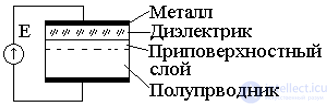
The processes occurring in an MDS system are related to the field effect. The field effect consists in a change in the concentration of charge carriers, and consequently in the conductivity, of the near-surface layer of the semiconductor under the action of an electric field created by a voltage E (Fig.).
Electrical Junctions in Semiconductors: The P-n Junction, Its Formation and Key Parameters, I-V Characteristic, Capacitance, and Breakdown

Enrichment mode and depletion mode. A near-surface layer with an increased concentration of free charge carriers is called enriched, and one with a decreased concentration is called depleted.
Electrical Junctions in Semiconductors: The P-n Junction, Its Formation and Key Parameters, I-V Characteristic, Capacitance, and Breakdown

P-n junction

A p-n junction cannot be obtained by mechanically contacting two semiconductors with different types of conductivity, because:

  • a) the surfaces of semiconductors are covered with an oxide layer, which is a dielectric.
  • b) there is always an air gap exceeding the interatomic distance.

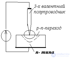
Two methods of obtaining a p-n junction are most widespread.

a) The fusion (alloying) method.

b) The diffusion method.

Let us consider method (b). The planar design of p-n junctions is the most common, in which the p-n junction is created by diffusion into one of the sides of a semiconductor wafer.
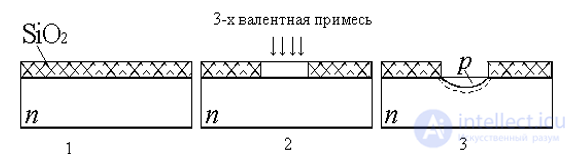
  • 1. A thin wafer is subjected to heat treatment, as a result of which a layer of silicon dioxide SiO2 - an insulator - appears.
  • 2. Using photolithography methods, certain areas of the SiO2 layer are removed, creating windows, and an acceptor impurity is deposited into them.
  • 3. As a result of diffusion of impurity atoms into the n-type semiconductor, a p-region is formed, and a p-n junction forms between them. p-n junction.

Electrical Junctions in Semiconductors: The P-n Junction, Its Formation and Key Parameters, I-V Characteristic, Capacitance, and BreakdownElectrical Junctions in Semiconductors: The P-n Junction, Its Formation and Key Parameters, I-V Characteristic, Capacitance, and Breakdown

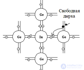
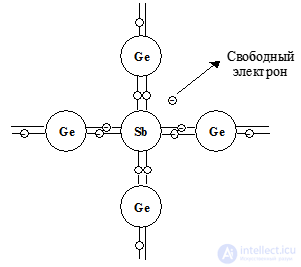
a) b)

Formation and main parameters of a p-n junction

The main element of most semiconductor devices, such as diodes, is the electron-hole junction (p-n junction).
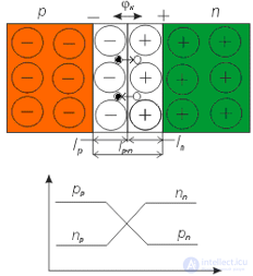
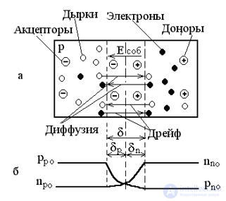
A p-n junction is a transition layer lp-n (Fig. 1.1) between two regions of a semiconductor with different types of electrical conductivity, depleted of free charge carriers, with its own diffusion electric field Ediff, which arises due to the contact potential difference φk, and impedes the diffusion of majority charge carriers while accelerating minority carriers.
Electrical Junctions in Semiconductors: The P-n Junction, Its Formation and Key Parameters, I-V Characteristic, Capacitance, and Breakdown

The p-n junction is characterized by two main parameters:

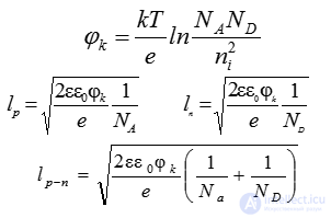
1. The contact potential difference φk, also called the height of the potential barrier. This is the energy that a free charge must have in order to overcome the potential barrier:

where Na, ND are the concentrations of the acceptor and donor impurities; k is the Boltzmann constant; e is the electron charge; T is the temperature; are the concentrations of acceptors and donors in the hole and electron regions, respectively; pp and pn are the concentrations of holes in the p- and n-regions, respectively; ni is the intrinsic concentration of charge carriers in an undoped semiconductor,

jT = kT/e is the thermal potential. At a temperature of T=27°C, jT=0.025V, while jk=0.3-0.3V for Ge, and jk=0.6-0.8V for a silicon (Si) junction.

2. The width of the p-n junction lp-n = lp + ln: - this is the boundary region depleted of charge carriers, located in the p- and n-regions:

where ε is the relative permittivity of the semiconductor material; ε0 is the permittivity of free space.

The thickness of electron-hole junctions is on the order of lp-n = (0.1-10) μm; it is proportional to the voltage across the p-n junction and inversely proportional to the impurity concentration in the p- and n-regions.

If the impurity concentrations are equal, the p-n junction is called symmetric; if they are not, the p-n junction is called asymmetric, and in this case it is located mainly in the region of the semiconductor with the lower impurity concentration.
Electrical Junctions in Semiconductors: The P-n Junction, Its Formation and Key Parameters, I-V Characteristic, Capacitance, and Breakdown

Currents of the p-n junction

There are three modes of operation of a p-n junction
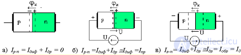
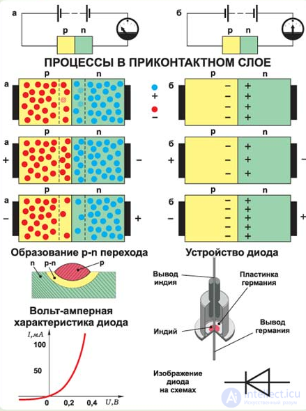
1. P-n junction in equilibrium state: Up-n= φk, (fig. a)
Without an external voltage applied to the p- and n-regions, two currents flow through the p-n junction: the diffusion current Idiff and the drift current Idr. The diffusion current is created by majority charge carriers, while the drift current is created by minority carriers.
In the equilibrium state, the sum of the diffusion and drift currents equals zero:

Ip-n = Idiff + Idr = 0

This relation is called the condition of dynamic equilibrium of diffusion and drift processes in an isolated (equilibrium) p-n junction.
Electrical Junctions in Semiconductors: The P-n Junction, Its Formation and Key Parameters, I-V Characteristic, Capacitance, and Breakdown
2) The p-n junction is forward biased: Up-n= φk-U, (fig. b). Ip-n = Ifwd
Injection - the process of converting majority charge carriers into minority carriers as forward current flows. The width of the p-n junction decreases:
lp-n ~(φk-U)1/2.
3) The p-n junction is reverse biased: Up-n= φk+U, (fig. c). Ip-n = Irev

Extraction - the process of converting minority charge carriers into majority carriers as reverse current flows. The width of the p-n junction increases:

lp-n ~(φk+U)1/2

The I-V characteristic of the p-n junction

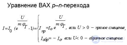
The current-voltage (I-V) characteristic of a p-n junction is the dependence of the current through the junction on the voltage applied to it, i=f(u).

Analytically, for forward and reverse bias, the I-V characteristic is written as:
Electrical Junctions in Semiconductors: The P-n Junction, Its Formation and Key Parameters, I-V Characteristic, Capacitance, and Breakdown

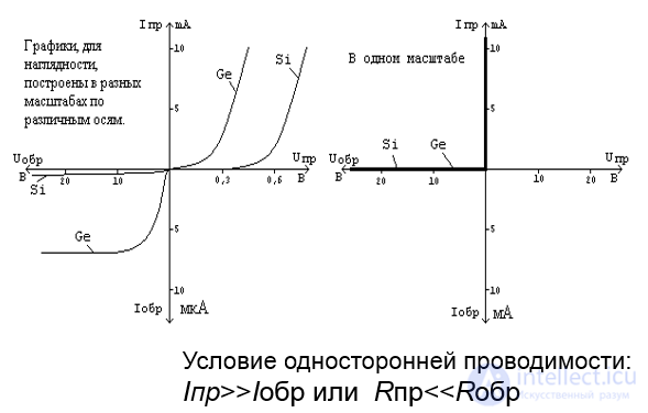
For clarity, the I-V characteristic is represented in the form of graphs (fig. 1.3).
Electrical Junctions in Semiconductors: The P-n Junction, Its Formation and Key Parameters, I-V Characteristic, Capacitance, and Breakdown

If the forward and reverse branches are plotted on the same scale, the I-V characteristic of the p-n junction has the form shown in fig. a. The figure clearly shows that the p-n junction has one-way conductivity, i.e., Ifwd >> Irev, or Rfwd <

To study the features of the forward and reverse branches of the I-V characteristic, they are plotted on different scales; for example, the current scales may differ by a factor of a thousand.


The graph shows that the forward branch of the I-V characteristic of a silicon-based diode is shifted to the right, while its reverse branch has a current much smaller than that of a germanium diode.

The differential resistance of the p-n junction under forward bias is determined from the relation rdiff= φT/I.

For example, at I=1mA and φT=25mV, rdiff=25Ohm.

Capacitances of the p-n junction

The fact that near the p-n junction there are uncompensated electric charges indicates that it has capacitance. The capacitance of the p-n junction consists of two components - the barrier capacitance Cbar and the diffusion capacitance Cdiff are distinguished.

Electrical Junctions in Semiconductors: The P-n Junction, Its Formation and Key Parameters, I-V Characteristic, Capacitance, and Breakdown

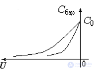
a) Under reverse bias, the barrier capacitance predominates, Cbar > Cdiff.
Electrical Junctions in Semiconductors: The P-n Junction, Its Formation and Key Parameters, I-V Characteristic, Capacitance, and Breakdown

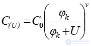
It is associated with immobile impurity ions, whose concentration is small. The magnitude of this capacitance depends on the magnitude of the voltage U across the p-n junction, on the junction area S, and also on the impurity concentration.
Electrical Junctions in Semiconductors: The P-n Junction, Its Formation and Key Parameters, I-V Characteristic, Capacitance, and BreakdownElectrical Junctions in Semiconductors: The P-n Junction, Its Formation and Key Parameters, I-V Characteristic, Capacitance, and Breakdown

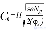
where C0 is the capacitance at zero voltage, - is the reverse voltage,

the exponent depends on the type of p-n junction (n=1/2 for an abrupt junction, n=1/3 for a graded junction),

ε is the permittivity of the semiconductor material;

S is the area of the p-n junction.

A model analog of the barrier capacitance can be the capacitance of a parallel-plate capacitor whose plates are the p- and n-regions, and whose dielectric is the p-n junction, which has practically no mobile charges. The value of the barrier capacitance ranges from tens to hundreds of picofarads, and the change in this capacitance with changing voltage can reach a factor of ten.

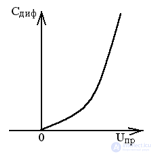
b) Diffusion capacitance predominates (Cdiff >> Cbar) under forward bias of the p-n junction.

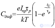
It is characterized by the accumulation of minority charge carriers near the p-n junction as the forward diffusion current (injection current) flows
Electrical Junctions in Semiconductors: The P-n Junction, Its Formation and Key Parameters, I-V Characteristic, Capacitance, and Breakdown

where is the lifetime of minority charge carriers,

is the time during which the forward current Ifwd flows.

The values of the diffusion capacitance can be on the order of hundreds to thousands of picofarads.

Overall, comparing the diffusion and barrier capacitances, Cdiff >> Cbar.

This is because the diffusion capacitance is associated with the forward, diffusion current (the current of majority charge carriers), which can reach large values.
Electrical Junctions in Semiconductors: The P-n Junction, Its Formation and Key Parameters, I-V Characteristic, Capacitance, and Breakdown

In practice, the barrier capacitance is used, since the diffusion capacitance has a low quality factor, because a forward-biased p-n junction with low forward resistance is connected in parallel with this capacitance.

Breakdown of the p-n junction

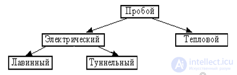
A sharp increase in current under reverse bias of the p-n junction is called breakdown of the p-n junction, and the voltage at which this occurs is called the
Electrical Junctions in Semiconductors: The P-n Junction, Its Formation and Key Parameters, I-V Characteristic, Capacitance, and Breakdown

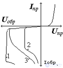
1. Electrical breakdown - reversible, i.e., it does not lead to the destruction of the p-n junction; when the reverse voltage decreases, the p-n junction recovers its properties;

It can be tunnel breakdown - curve 2, or avalanche breakdown - curve 1. Avalanche breakdown arises due to avalanche multiplication of minority charge carriers by impact ionization. Tunnel breakdown arises due to the transition of electrons from a bound state to a free state without imparting additional energy to them.

2. Thermal breakdown - irreversible, leads to the destruction of the p-n junction - curve 3.
Electrical Junctions in Semiconductors: The P-n Junction, Its Formation and Key Parameters, I-V Characteristic, Capacitance, and Breakdown

Additional materials

Electrical Junctions in Semiconductors: The P-n Junction, Its Formation and Key Parameters, I-V Characteristic, Capacitance, and BreakdownElectrical Junctions in Semiconductors: The P-n Junction, Its Formation and Key Parameters, I-V Characteristic, Capacitance, and Breakdown

Electrical Junctions in Semiconductors: The P-n Junction, Its Formation and Key Parameters, I-V Characteristic, Capacitance, and BreakdownElectrical Junctions in Semiconductors: The P-n Junction, Its Formation and Key Parameters, I-V Characteristic, Capacitance, and Breakdown

See also

  • Semiconductor devices
  • Semiconductor device
  • Diode
  • Transistor
  • Integrated circuit

Comments

To leave a comment

If you have any suggestion, idea, thanks or comment, feel free to write. We really value feedback and are glad to hear your opinion.
To reply

Lectures and tutorial on "Electronics, Microelectronics, Element Base"

Terms: Electronics, Microelectronics, Element Base