
Lecture
Phototransistor is a radiation-controlled device with two or more mutually interacting electrical junctions. It is used as the radiation-sensitive element in optoelectronic pairs and photodetector devices, as a primary transducer in measurement and information systems, as an element of the receiving module in medium-throughput fiber-optic communication lines, and in other applications. Bipolar and field-effect phototransistors are distinguished. The photothyristor is also classified among phototransistors.
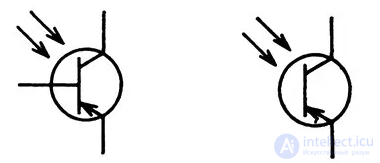
Schematic representation of a phototransistor in electrical circuit diagrams
VT1 – phototransistors with a base lead, VT2 – phototransistors without a base lead.
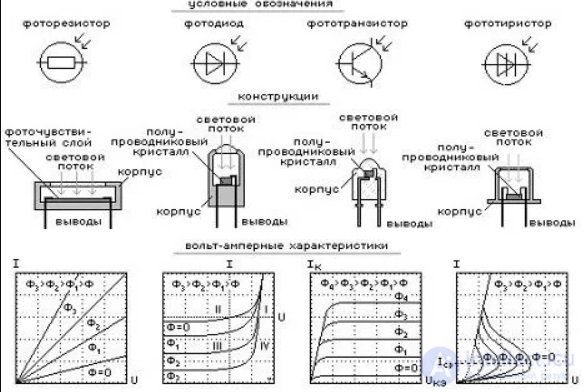
The phototransistor was invented by John Northrup Shive (John Northrup Shive) in 1948 while he was working at Bell Laboratories, but the invention was not announced until 1950. At that same time, phototransistors were first used in a punched-card reader at an automatic telephone exchange.
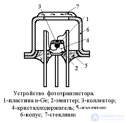 Fig. 1
One of the possible design variants of a phototransistor is shown in Fig. 1. As can be seen from this figure, a phototransistor differs from an ordinary transistor only in the transparent window in its case; through this window the light flux falls on the semiconductor wafer that serves as the base, in the center of which the collector junction is formed by alloying.
Other electrode arrangements are also possible, for example a ring-shaped collector on the illuminated surface of the base.
The design and connection circuit of a bipolar phototransistor are also shown in Fig. 2.a.
A phototransistor consists of:
1 - the emitter region of p+ type;
2 - the base region of n type, most of which is passive and exposed to the light flux;
3 - the wide collector region of p type.
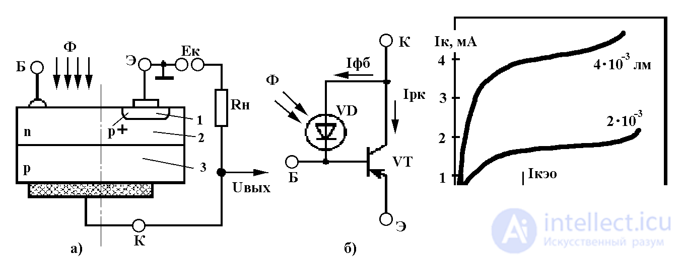 Fig. 2
The passive part of the base is located in Fig. 2.a to the left of the dash-dotted line. A phototransistor is usually connected in a common-emitter (CE) configuration with a load resistor RL in the collector circuit (Fig. 2.a). The input signal of the phototransistor is the modulated light flux, and the output is the change in voltage at its collector.
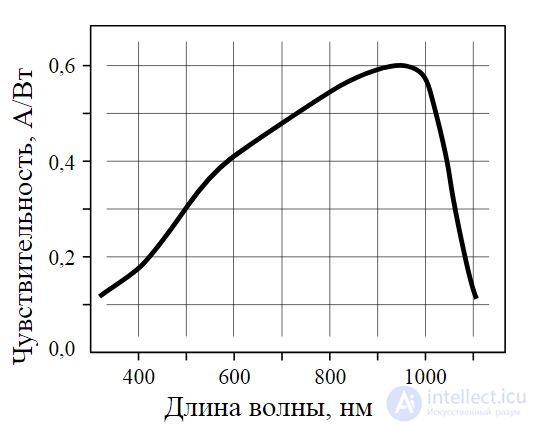
Typical spectral sensitivity of a silicon phototransistor
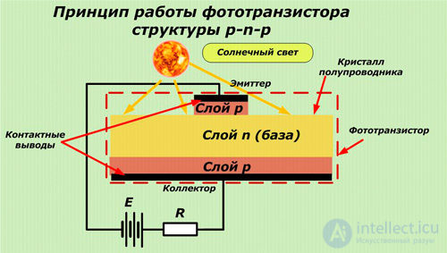
Let us consider the operating principle of a phototransistor in a circuit with an open base lead. The optical signal generates carriers in the collector junction and in the passive base region. These carriers diffuse through the base toward the collector junction and are separated by its electric field. The minority carriers create the photocurrent of the collector junction, while the majority carriers accumulate in the base and compensate the charge of the fixed impurity ions at the boundary of the emitter junction. The potential barrier of the junction is lowered, which enhances the injection of carriers from the emitter into the base. The injected carriers diffuse through the base toward the collector junction and are drawn by its electric field into the collector region. The current of the injected carriers, and correspondingly the collector current they form, exceeds the photocurrent of the optically generated carriers many times over.
The total collector current is the sum of the photocurrent Ipb and the current Icr of holes injected by the emitter that have passed through the collector junction.
The photocurrent gain coefficient:
M=(Ipv+Icr)/Ipb=β+1, if  , (1)
, (1)
where β is the static current transfer coefficient of the transistor in a common-emitter configuration.
The photocurrent, amplified M times, produces a voltage drop across the load resistor RL, changing the collector voltage by:
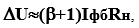 , (2)
, (2)
From this relationship it follows that a phototransistor can be represented as an equivalent photodiode VD and an amplifying transistor VT (Fig. 2.b). The equivalent photodiode is formed by the passive base and the collector region to the left of the dash-dotted line in Fig. 2.a, while the structure of the amplifying transistor is located to the right of this line. The transistor increases the sensitivity of the equivalent photodiode by a factor of ( β+1).
The base lead B of the phototransistor is sometimes used to apply a bias when selecting the operating point on the input and output characteristics of the transistor and to ensure its temperature stabilization.
The family of output characteristics of a phototransistor in a common-emitter configuration is shown in Fig. 2.c. The photocurrent is formed by nonequilibrium carriers generated in the base region.
The light characteristic of a phototransistor is the dependence of the collector current on the light flux, Ic=f(Φ). It is linear only at low flux levels. As the light flux increases and the concentration of nonequilibrium carriers in the base grows, the probability of their recombination increases, and the transfer and injection coefficients of the phototransistor decrease. The direct proportionality between the collector current and the light flux breaks down.
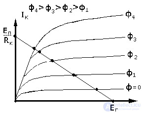 Fig. 3
Most parameters of a bipolar phototransistor are analogous in physical meaning to the parameters of photodiodes. In addition, the phototransistor is characterized by its operating supply voltage, junction capacitances Cc and Ce, static current gain, and other parameters of an ordinary transistor.
The current-voltage characteristics of a phototransistor (Fig. 3) resemble the output characteristics of an ordinary transistor in a common-emitter configuration, but here the parameter is not the current IC, but the light flux Φ.
The steep initial section of these characteristics corresponds to the saturation mode: at low Uce values, the collector junction, as in a bipolar transistor, opens due to the accumulation of holes in the collector. The slope of the characteristics toward the abscissa axis in their flatter portion is explained, as with the bipolar transistor, by the base-width modulation effect.
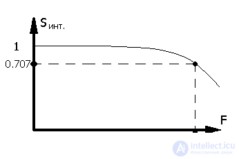 Fig. 4
The frequency properties of phototransistors are determined mainly by the diffusive motion of carriers in the base of the device and by the charging processes of the junction capacitances.
As the modulation frequency of the light flux increases, the photocurrent decreases, just as it does in photodiodes (Fig. 4).
One of the most important parameters of a phototransistor is the photocurrent gain coefficient of the phototransistor (Kpg) - the ratio of the collector photocurrent of the phototransistor with the base disconnected to the photocurrent of the illuminated p-n junction measured in diode mode:
 , (3)
, (3)
The current sensitivity of a phototransistor is the ratio of the change in electric current at the output of the phototransistor to the change in radiant flux, with an open circuit at the input and a short circuit at the output for AC current. For a common-emitter circuit, the current sensitivity equals:
 (4)
(4)
The emitter junction of a bipolar phototransistor is connected in the forward direction. Its specific capacitance is about 105  . The charging time constant of the emitter junction capacitance increases as the light flux intensity decreases. At low light fluxes, this time constant mainly determines the inertia of the phototransistor. At high light fluxes, the inertia of the phototransistor is affected by the carrier diffusion time in the base and by the collector junction capacitance. For this reason, materials with high carrier mobility are chosen for phototransistors, and structures with an internal electric field in the base or with a thin base are used. Reducing the collector junction capacitance by lowering the impurity concentration in the collector region is possible only up to a certain limit. Reducing the area of the equivalent photodiode for this purpose is impractical, since it lowers the sensitivity of the phototransistor.
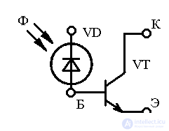
Fig. 5
To increase the sensitivity of a phototransistor, the base thickness and carrier lifetime in the base must be increased, and consequently materials with high resistivity must be chosen. But to increase its cutoff frequency, the base thickness and carrier lifetime must be reduced. The contradiction between speed and sensitivity is resolved by the photodiode-transistor structure, whose equivalent circuit is shown in Fig. 5. Both elements of the structure are fabricated on a single chip. The parameters of the photodiode are chosen to achieve maximum sensitivity and speed, while the parameters of the transistor are chosen for maximum cutoff frequency and gain. Together, both elements are equivalent to a high-speed phototransistor with a high gain coefficient
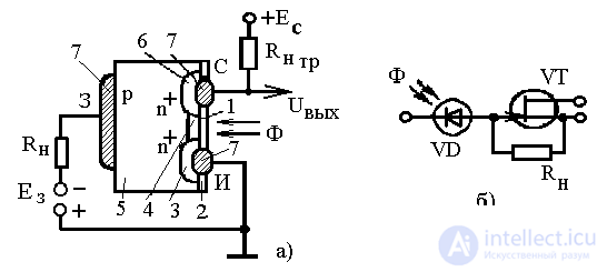
Fig. 6
The design and connection circuit of a field-effect phototransistor with a controlling p-n junction are shown in Fig. 6.a
where: 1 - anti-reflective coating;
2 - dielectric layer;
3 - source region of n+ type;
4 - channel of n type;
5 - gate region of p type;
6 - drain region of n+ type;
7 - device leads;
RL - load resistor in the gate circuit;
RL.tr - load resistor of the phototransistor.
The light flux generates nonequilibrium carriers in gate region 3 and in the gate-channel p-n junction. The electric field of this junction separates the nonequilibrium carriers. A photocurrent Iph. appears in the gate circuit. It produces a voltage drop across resistor RL:
 (5)
(5)
The gate voltage increases, and the drain current changes by:
 , (6)
, (6)
where S is the transconductance of the drain-gate characteristic of the field-effect transistor. The channel conductivity increases, and the drain voltage correspondingly decreases by:
 , (7)
, (7)
The change in drain voltage is the output electrical signal of the circuit. Thus, a field-effect phototransistor is equivalent to a "gate-channel" photodiode and an amplifying field-effect transistor with a controlling p-n junction (Fig. 6.b).
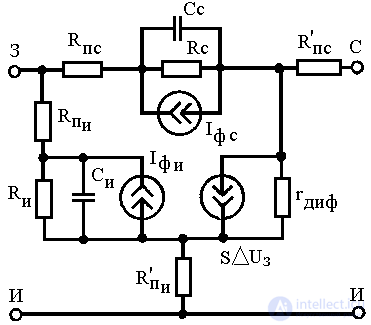 Fig. 7
In the equivalent circuit of a field-effect phototransistor (Fig. 7), sources Ips and Ipd model the photocurrents of the "source-gate" and "drain-gate" p-n junctions; source SUg represents the gain in the transistor; resistor rDIFF is the differential output resistance of the transistor; resistors Rs, Rd and capacitors Cs, Cd account for the resistance and capacitance of the junctions between the "source-gate" and "drain-gate" regions. Resistors Rgd, Rgs, R`gd, R`gs, taking into account the resistance of the ohmic contacts, determine the series-connected resistances of the regions between the gate lead and the drain region, the gate lead and the source region, the source lead and the gate region, and the drain lead and the gate region. For the current source in the output circuit of the phototransistor, one can write:
 , (8)
, (8)
where Ip.c. is the photocurrent of the "channel-gate" p-n junction.
When the "gate-source" circuit is short-circuited, the bulk resistances Rgs, R`gs, Rgd act as load resistors. The time constants (Rgs+R`gs)Cs and (Rgd+R`gd)Cd, as well as the carrier transit time in the channel, determine the ultimate speed of the phototransistor.
The parameters of a field-effect phototransistor are analogous in physical meaning to those of a bipolar phototransistor.
The structures of p-n junction field-effect transistors and MOS phototransistors are diverse. The highest speed and sensitivity are found in the photodiode - field-effect transistor structure. The photodiode is combined with the source region of the field-effect transistor, the amplifying element. Each component of the structure is optimized separately: the photodiode for sensitivity and speed, the field-effect transistor for cutoff frequency and gain.
A comparative evaluation of phototransistor parameters shows that the composite phototransistor has the highest sensitivity, while the photodiode-bipolar transistor (PD-BT) structure offers the best speed combined with good sensitivity. The photodiode-field-effect transistor structure has parameters close to those of the PD-BT structure. Phototransistors are inferior to photodiodes in speed, but thanks to signal amplification they have high sensitivity.
Phototransistors have an operating range whose size depends on the intensity of the incident light, since this is related to the positive potential of its base.
The base current produced by incident light is amplified hundreds and thousands of times. Additional current amplification is provided by a special Darlington transistor, which is a semiconductor whose emitter is connected to the base of another bipolar transistor. The diagram shows this type of phototransistor.
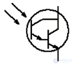
This makes it possible to achieve increased sensitivity in low light, since double amplification occurs through two semiconductors. With two transistors, amplification of hundreds of thousands of times can be achieved. It should be noted that the Darlington transistor reacts to light more slowly than an ordinary phototransistor.
Common-emitter circuit
In this circuit, the output signal transitions from a high state to a low state when light rays fall on the device.
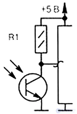
This circuit is implemented by connecting a resistor between the transistor's collector and the power supply. The output voltage is taken from the collector.
Common-collector circuit
An amplifier connected in a common-collector configuration produces an output signal that transitions from a low state to a high state when light strikes the semiconductor.
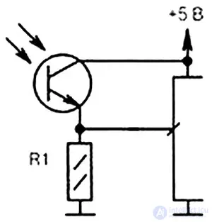
This circuit is formed by connecting a resistor between the negative supply lead and the emitter. The output signal is taken from the emitter.
In both variants, the transistor can operate in 2 modes:
Active mode
In this mode, the phototransistor produces an output signal that depends on the intensity of the incident light. When the illumination level exceeds a certain threshold, the transistor saturates, and the output signal will no longer increase even if the intensity of the light rays is increased. This mode of operation is recommended for devices with the function of comparing two light-flux thresholds.
Switching mode
The operation of the semiconductor in this mode means that the transistor will respond to the application of light by turning off or on. This mode is necessary for devices that require an output signal in digital form. By changing the value of the resistor in the amplifier circuit, one of the operating modes can be selected.
For operating a phototransistor as a switch, a resistance of more than 5 kΩ is most often used. The high-level output voltage in switching mode will equal the supply voltage. The low-level output voltage should be less than 0.8 V.
Testing a phototransistor
Such a transistor is easily tested with a multimeter, even without access to the transistor's base lead. If a multimeter is connected to the emitter-collector section, its resistance at either polarity will be high, since the transistor is closed. If a beam of light falls on the sensitive element, the measuring instrument will show a low resistance value, since the transistor opens in this case due to the light, provided the supply polarity is correct.
An ordinary transistor behaves the same way, but it is opened by an electric current signal rather than by a beam of light. Besides the intensity of the light, the spectral composition of the light also plays a major role.
Devices designed to receive external radiation are enclosed in a plastic, metal-glass, or metal-ceramic case with a transparent window or lens made of plastic or glass. An exception is made for phototransistors that are part of optocouplers, which are enclosed together with the radiation source in an opaque case.
Devices housed in metal-glass and metal-ceramic cases usually have an electrical base lead.
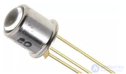
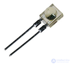
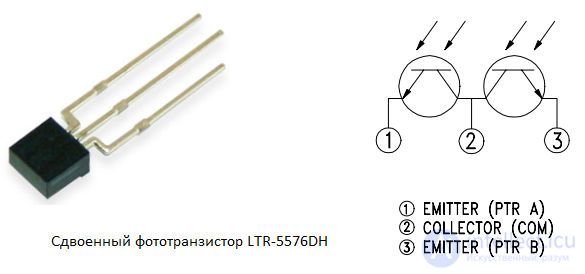
Dual phototransistor
Advantages of phototransistors
Disadvantages of phototransistors
Phototransistors are analogous to photodiodes, but they have serious drawbacks that limit this semiconductor to narrow specialized applications.
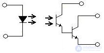
An optocoupler with a composite phototransistor-transistor pair in a Darlington configuration
Since phototransistors are more sensitive than photodiodes, they are conveniently used as radiation receivers in various automatic safety systems, security alarm systems, punched card and punched tape readers, position and distance sensors, and other applications where high speed is not critical.
Phototransistors are often used in optocouplers as the radiation receivers in optoisolators.
Phototransistors are also used in


Comments