
Lecture
An organic field-effect transistor (OFET) is a field-effect transistor that uses an organic semiconductor in its channel. OFETs can be produced either by evaporating small molecules in a vacuum, by casting polymers or small molecules from solution, or by mechanically transferring an exfoliated single-crystal organic layer onto a substrate. These devices were developed to enable inexpensive, large-area electronic products and biodegradable electronics. OFETs are fabricated with a variety of device geometries. The most commonly used device geometry is a bottom gate with top drain and source electrodes, because this geometry is analogous to that of a thin-film silicon transistor (TFT) using thermally grown SiO2 as the gate dielectric. Organic polymers, such as polymethyl methacrylate (PMMA), can also be used as the dielectric. One advantage of OFETs, particularly compared to inorganic TFTs, is their unprecedented physical flexibility, which leads to biocompatible applications, for example in the future personalized-biomedicine and bioelectronics healthcare industry.
In May 2007, Sony reported the first full-color, flexible, all-plastic display with high video refresh rates, in which both the thin-film transistors and the light-emitting pixels were made from organic materials.
The concept of the field-effect transistor (FET) was first proposed by Julius Edgar Lilienfeld, who was granted a patent on his idea in 1930. He proposed that the field-effect transistor behaves like a capacitor with a conducting channel between the source and drain electrodes. The voltage applied to the gate electrode controls the amount of charge carriers flowing through the system.
The first field-effect transistor was developed and fabricated by Mohamed Atalla and Dawon Kahng at Bell Labs using a metal-oxide-semiconductor field-effect transistor: the MOSFET (metal-oxide-semiconductor field-effect transistor). It was invented in 1959 and presented in 1960. Also known simply as the MOS transistor, the MOSFET is the most widely manufactured device in the world. [10] The concept of the thin-film transistor (TFT) was first proposed by Paul K. Weimer in 1962.[11] The TFT is a particular type of MOSFET.[12]
Rising material and manufacturing costs,[edit] along with growing public interest in more environmentally friendly electronic materials, have supported the development of organic-based electronics in more recent years. In 1986, Mitsubishi Electric researchers H. Koezuka, A. Tsumura, and Tsuneya Ando reported the first organic field-effect transistor,[13] [14] based on a polymer made of thiophene molecules.[15] The thiophene polymer is a type of conjugated polymer that is able to conduct charge, eliminating the need to use expensive metal-oxide semiconductors. In addition, other conjugated polymers have been shown to possess semiconducting properties. OFET design has also improved over the last few decades. Many OFETs are now being developed based on the thin-film transistor (TFT) model, which allows less conductive materials to be used in the device design. Over the last several years, these models have been refined with respect to field mobility and on/off current ratios.
One common feature of OFET materials is the incorporation of an aromatic or otherwise conjugated π-electron system, which facilitates delocalization of the orbital wave functions. Electron-donating or electron-withdrawing groups may be attached to facilitate hole or electron transport.
OFETs using a wide range of aromatic and conjugated materials as the active semiconducting layer have been reported, including small molecules such as rubrene, tetracene, pentacene, diindenoperylene, perylenediimides, tetracyanoquinodimethane (TCNQ), and polymers such as polythiophene (especially poly(3-hexylthiophene) (P3HT)), polyfluorene, polydiacetylene, poly(2,5-thienylene vinylene), and poly(p-phenylene vinylene) (PPV).
This field is very active, with newly synthesized and tested compounds reported weekly in leading research journals. There are numerous review articles documenting the development of these materials.[16] [17] [18] [19] [20]
Rubrene-based OFETs exhibit the highest carrier mobility, 20–40 cm2/(V·s). Another popular OFET material is pentacene, which has been used since the 1980s, but its mobility is 10–100 times lower (depending on the substrate) than that of rubrene.[20] The main problem with pentacene, as with many other organic conductors, is its rapid oxidation in air to form pentacenequinone. However, if the pentacene is pre-oxidized and the pentacenequinone thus formed is used as the gate insulator, the mobility can approach values comparable to rubrene. This method of oxidizing pentacene is akin to the oxidation of silicon used in silicon electronics.[16]
Polycrystalline tetrathiafulvalene and its analogs provide mobilities in the range of 0.1–1.4 cm2/(V·s). However, mobility exceeding 10 cm2/(V·s) has been achieved in single-crystal hexamethylenetetrathiafulvalene (HMTTF) grown from solution or by vapor transport. The turn-on/turn-off voltage differs for devices grown using these two techniques, presumably due to the higher processing temperatures used when increasing vapor transport.[16]
All of the devices mentioned above are based on p-type conductivity. N-type OFETs remain poorly developed. They are typically based on perylenediimides or fullerenes or their derivatives and show electron mobilities below 2 cm2/(V·s).[17]
The three main components of a field-effect transistor are the source, drain, and gate. Field-effect transistors generally operate as a capacitor. They consist of two plates. One plate acts as a conducting channel between two ohmic contacts, which are called the source and drain contacts. The other plate controls the charge induced in the channel and is called the gate. The direction of carrier movement in the channel is from the source to the drain. Accordingly, the relationship among these three components is that the gate controls the movement of carriers from the source to the drain.[21]
When this capacitor concept is applied to device design, different devices can be built based on differences in the controller, i.e., the gate. This can involve the gate material, the position of the gate relative to the channel, how the gate is insulated from the channel, and what type of carrier is induced in the channel by the gate voltage (for example, electrons in an n-channel device, holes in a p-channel device, and both electrons and holes in a dual-injection device).
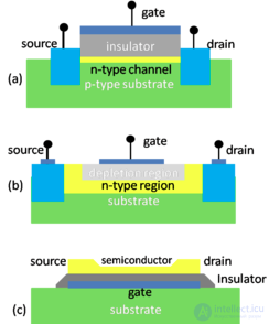
Figure 1. Diagram of three types of field-effect transistors (FETs):
(a) metal-insulator-semiconductor field-effect transistor (MISFET);
(b) metal-semiconductor field-effect transistor (MESFET);
(c) thin-film transistor (TFT).
Three types of field-effect transistors, classified by carrier properties, are shown schematically in Figure 1. These are the MOSFET (metal-oxide-semiconductor field-effect transistor), the MESFET (metal-semiconductor field-effect transistor), and the TFT (thin-film transistor).
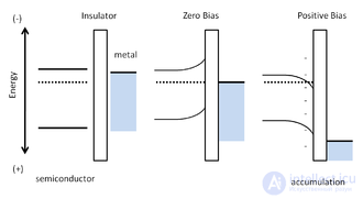
The best-known and most widely used field-effect transistor in modern microelectronics is the MOSFET (metal-oxide-semiconductor field-effect transistor). Within this category there are various types, such as the MISFET (metal-insulator-semiconductor field-effect transistor) and the IGFET (insulated-gate field-effect transistor). The MISFET structure is shown in Figure 1a. The source and drain are connected by a semiconductor, and the gate is separated from the channel by an insulating layer. If no bias (potential difference) is applied to the gate, band bending is induced due to the difference between the energy of the metal's conduction band and the Fermi level of the semiconductor. As a result, a higher concentration of holes forms at the semiconductor-dielectric interface. When a sufficient positive bias is applied to the gate contact, the bent band becomes flat. If a larger positive bias is applied, the band bends in the opposite direction, and the region near the dielectric-semiconductor interface becomes depleted of holes. A depletion region then forms. With an even larger positive bias, the band bending becomes so large that the Fermi level at the semiconductor-dielectric interface moves closer to the bottom of the conduction band than to the top of the valence band, so it forms an inversion layer of electrons, providing a conducting channel. Finally, this turns the device on.
The second type of device is shown in Figure 1b. The only difference from the MISFET is that the n-type source and drain are connected by an n-type region. In this case, the depletion region extends across the entire n-type channel at zero gate voltage in a normally-off device (this is similar to the larger positive bias case in the MISFET). In a normally-"on" device, part of the channel is not depleted, which results in current flow at zero gate voltage.
The thin-film transistor (TFT) is shown in Figure 1c. Here, the source and drain electrodes are deposited directly onto the conducting channel (a thin semiconductor layer), and then a thin insulating film is deposited between the semiconductor and the metal gate contact. This structure implies that there is no depletion region separating the device from the substrate. If there is zero bias, electrons are pushed away from the surface due to the difference between the Fermi levels of the semiconductor and the metal. This causes bending of the semiconductor bands. In this case, there is no carrier movement between the source and drain. When a positive charge is applied, the accumulation of electrons at the interface causes the semiconductor to bend in the opposite direction and reduces the conduction band relative to the semiconductor's Fermi level. A highly conductive channel then forms at the interface (shown in Figure 2).
OFETs use the TFT architecture. With the development of conducting polymers, semiconducting properties were discovered in small conjugated molecules. Interest in OFETs has grown considerably over the last decade. The reasons for this surge in interest are varied. The performance of OFETs, which can compete with that of amorphous-silicon (a-Si) TFTs having a field mobility of 0.5–1 cm2 V−1 s−1 and on/off current ratios (which indicate the device's ability to switch off) of 106–108, has improved significantly. Currently, the mobility of OFET thin films is 5 cm2 V-1 s-1 in the case of vacuum-deposited small molecules[24] and 0.6 cm2 V-1 s-1 for solution-processed polymers[25]. As a result, there is now greater industrial interest in using OFETs for applications that are currently incompatible with a-Si or other inorganic transistor technologies. One of their main technological advantages is that all OFET layers can be deposited and patterned at room temperature by combining inexpensive solution processing with direct-write printing, making them ideally suited for realizing inexpensive, large-area electronic functions on flexible substrates.[26]
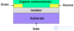
Thermally oxidized silicon is the traditional substrate for OFETs, where the silicon dioxide serves as the gate insulator. The active layer of the field-effect transistor is usually deposited onto this substrate using either (i) thermal evaporation, (ii) coating from an organic solution, or (iii) electrostatic lamination. The first two methods result in polycrystalline active layers; they are much easier to produce, but have relatively low transistor performance. Numerous variations of the solution-coating technique (ii) are known, including dip coating, spin coating, inkjet printing, and screen printing. The electrostatic lamination technique is based on manually peeling a thin layer from an organic single crystal; this results in a superior single-crystal active layer, but is more laborious. The thickness of the gate oxide and the active layer is less than one micrometer.[16]
Carrier transport in OFETs is specific to two-dimensional (2D) carrier propagation within the device. Various experimental methods have been used to study this, such as the Haynes-Shockley time-of-flight experiment for injected carriers, the time-of-flight (TOF) experiment[27] for determining carrier mobility, the pressure-wave propagation experiment for studying the electric field distribution in dielectrics, the organic monolayer experiment for studying dipole orientation changes, time-resolved second-harmonic generation optics (TRM-SHG), and others. While carriers propagate through polycrystalline OFETs in a diffusive (trap-limited) manner,[28] they move through the conduction band in the best single-crystal OFETs.[16]
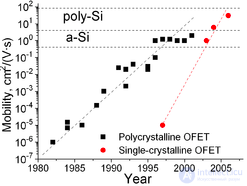
The most important carrier-transport parameter for an OFET is carrier mobility. Its evolution over the years of OFET research is shown on the graph for polycrystalline and single-crystal OFETs. Horizontal lines show comparative benchmarks for the main competitors of OFETs — amorphous (a-Si) and polycrystalline silicon. The graph shows that mobility in polycrystalline OFETs is comparable to that of a-Si, whereas the mobility in rubrene-based OFETs (20–40 cm2/(V·s)) approaches that of the best polysilicon devices.
Developing accurate models of charge-carrier mobility in OFETs is an active area of research. Fishchuk et al. developed an analytical model of carrier mobility in OFETs that accounts for carrier density and the polaron effect.
Although the average carrier density is usually calculated as a function of gate voltage for use as an input to carrier mobility models, modulated-amplitude reflectance spectroscopy (MARS) has been shown to provide a spatial map of carrier density in the OFET channel.
Because electric current flows through such a transistor, it can be used as a light-emitting device, thereby combining current modulation with light emission. In 2003, a German research group presented the first organic light-emitting field-effect transistor (OLET).[32] The device consists of interdigitated gold source and drain electrodes and a thin polycrystalline tetracene film. Both positive charges (holes) and negative charges (electrons) are injected from the gold contacts into this layer, resulting in electroluminescence of the tetracene.
[[b291]]
NOMFET

Comments