
Lecture
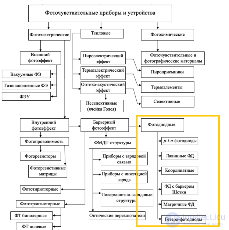
A photodiode is a photosensitive semiconductor diode with a p-n junction (between two types of semiconductor, or between a semiconductor and a metal).
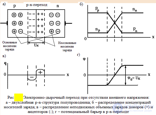
Under the action of light falling on the p-n junction, electron-hole pairs are formed in it. Minority carriers, i.e. holes in the n-region and electrons in the p-region, diffuse into the region of the p-n junction, are drawn in by its field, and are ejected into the region beyond the junction, forming a space charge there. As minority carriers move from one region to another, they accumulate in one part of the system under consideration, while majority carriers accumulate in the other part. This accumulation cannot continue indefinitely, because as the concentration of holes in the p-region and electrons in the n-region increases, so does the electric field they create, which opposes the transfer of minority carriers across the barrier layer from one region to the other. As this field increases, the reverse flow of carriers also increases. Eventually a dynamic equilibrium is reached, in which the number of minority carriers crossing the barrier layer per unit time equals the number of the same carriers moving in the opposite direction. In this state, a certain potential difference E is established between the electrodes — this is the photo-EMF. When a load is connected to the photodiode terminals, a current appears in its circuit, whose magnitude is determined by the difference between the opposing carrier flows across the p-n junction.
The structure of the photodiode junction is shown in Fig. 1a, and the family of current-voltage characteristics in Fig. 1b.
Photodiodes are used in photodiode (photoconductive) and photovoltaic modes. In the first, the diode is reverse-biased and the photocurrent is a function of the light flux. In the second mode, the device operates by generating a photo-EMF. Compared with the photovoltaic mode, the photodiode mode has a number of advantages: lower inertia, higher sensitivity to the long-wavelength part of the optical spectrum, and a wide dynamic range of characteristic linearity. The main drawback of this mode is the presence of noise current caused by fluctuations in the flow of charge carriers through the p-n junction as it flows through the load.
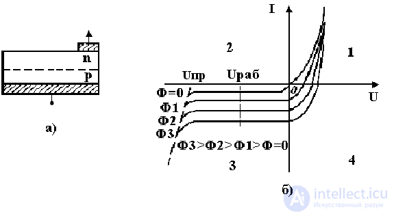 Fig. 1
In some cases, when a low noise level of the photodetector is required, the photovoltaic mode may prove more advantageous than the photodiode mode.
The current-voltage characteristics of the photodiode in quadrant I (see Fig. 1b) correspond to forward-direction connection. Quadrant IV corresponds to the diode operating in the photovoltaic mode, i.e. the photodiode acts as a solar converter, with the current and voltage depending on the intensity of the light flux. To extract maximum power at the load, the load resistance is taken equal to the internal resistance of the photodiode. Along the voltage axis one can determine the photo-EMF for various intensities of the incident light flux Φ at zero load resistance, and along the current axis the photocurrent for various values of Φ at zero load resistance. The characteristics in quadrant III correspond to the device operating in photodiode mode. The voltage UBR is the electrical breakdown voltage of the photodiode. The voltage UOP — the operating voltage — is specified in the datasheet.
The current-voltage characteristic in the absence of illumination is called the dark characteristic; in this case, the photodiode's current-voltage characteristic passes through 0 and coincides with the characteristic of an ordinary diode. The value of the dark current ID at a given ambient temperature and operating voltage is specified in the device's datasheet. The parameters of silicon and germanium photodiodes depend noticeably on the ambient temperature. For every 10° rise in temperature, the dark current of germanium devices increases by a factor of 2, and that of silicon devices by a factor of 2.5. At the same time, the sensitivity and detectivity decrease, the level of intrinsic noise increases, and the maximum of the spectral characteristic shifts toward shorter wavelengths. A decrease in temperature produces the opposite changes.
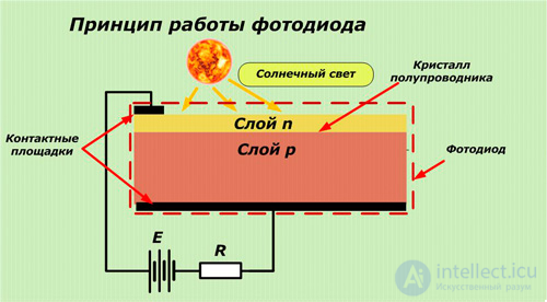
operating principle of a photodiode
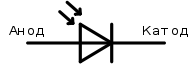
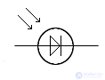
schematic symbol
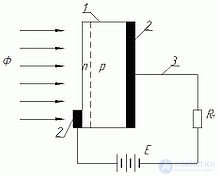
Structural diagram of a photodiode.
Φ — flux of electromagnetic radiation; E — DC source; RL — load.
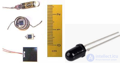
appearance of photodiodes
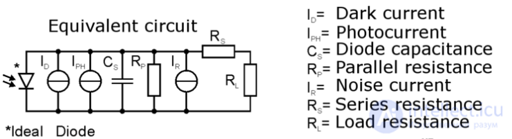
equivalent circuit of a photodiode
In a p-i-n structure, the middle i-region is sandwiched between two regions of opposite conductivity type. At a sufficiently high voltage, the field penetrates the i-region, and free carriers generated by photons under illumination are accelerated by the electric field of the p-n junctions. This yields a gain in speed and sensitivity. The increase in speed of a p-i-n photodiode is due to the fact that the diffusion process is replaced by drift of electric charges in a strong electric field. Already at Urev ≈ 0.1 V, the p-i-n photodiode has an advantage in speed.
These semiconductors are characterized by the presence, in the region of the p-n junction, of a section with intrinsic conductivity and a significant resistance value. When a light flux strikes this section, hole-electron pairs appear. The electric field in this region is constant, and there is no space charge. Such an auxiliary layer extends the range of operating frequencies of the semiconductor. By functional purpose, p-i-n photodiodes are divided into detector, mixer, parametric, limiter, multiplier, tuning, and other types.
This type is distinguished by high sensitivity. Its function is to convert a light flux into an electrical signal amplified via the avalanche multiplication effect. It can be used under conditions of very low light flux. The design of avalanche photodiodes uses superlattices, which help reduce interference during signal transmission.
Consists of a metal and a semiconductor, around whose junction boundary an electric field is created. The main difference from conventional p-i-n type photodiodes is the use of majority rather than minority charge carriers.
Formed from two semiconductors having different bandgap widths. The layer located between them is called heterogeneous. By selecting suitable semiconductors, a device can be created that operates over the entire wavelength range. Its drawback is the high complexity of manufacture.
Photodiodes are low-inertia photodetectors. Their inertia depends on the time characteristics of the carrier photogeneration process, the conditions for separating electron-hole pairs, the capacitance of the p-n junction, and the load resistance. In some cases, high speed is required of the photodevice (a few nanoseconds or less). Such devices are needed in optical communication lines, compact-disc sound reproduction systems, and others. In such devices, p-i-n structure photodiodes (i — dielectric) and avalanche photodiodes are used.
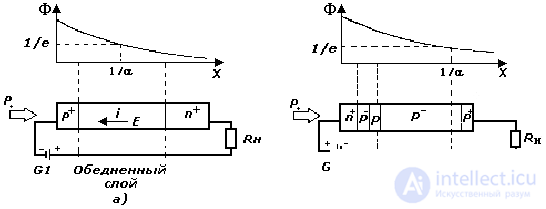 Fig. 3
p–i–n photodiodes. The structural diagram of a p-i-n photodiode is shown in Fig. 3a. On an n+ conductivity substrate, a lightly doped i-layer and a p+ conductivity layer up to 0.3 μm thick are formed. When reverse bias is applied, the entire i-layer becomes depleted. As a result, the junction capacitance decreases, the region of absorption of incident radiation expands, and the sensitivity of the device increases. The absorbed radiation decays exponentially within the structure (see Fig. 3) depending on the absorption coefficient, and causes photoexcited carriers to appear. The electric field of the depleted layer (field strength greater than or equal to 10^3 V/cm) accelerates them to the drift saturation velocity (about 10^7 cm/s). This region is called the drift space.
Outside the depleted layer, carrier motion is diffusive in nature, with a relatively low velocity — about 10^4 cm/s. This circumstance degrades the speed. To improve it, the absorption of radiation must be concentrated in the depleted layer. For this purpose, the p+ layer is made very thin, while the thickness of the i layer is made greater than the absorption length of the radiation  . The absorption length for silicon at a wavelength of 0.8 μm is approximately 10...20 μm, and the operating voltage at which the depleted layer has the required width does not exceed 10...20 V.
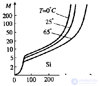 Fig. 4
Avalanche photodiodes (APD). APDs (see Fig. 3b) operate at reverse bias voltages sufficient for carrier multiplication. Compared with p–i–n photodiodes, they have internal gain and therefore greater sensitivity when receiving weaker signals. APDs are manufactured based on Ge, Si, group AIIIBV compounds, and other semiconductors. When selecting the photodiode material, the determining parameters are quantum efficiency in the given spectral range, speed, and noise. Germanium APDs provide high quantum efficiency in the spectral range of 1...1.6 μm, while silicon ones are especially effective at wavelengths of 0.6...1 μm. In an avalanche photodiode, radiation is absorbed in the depleted layer. To create impact ionization by photoexcited carriers, a region with a high electric field strength (greater than 10^5 V/cm) is formed next to the p-n junction, in which avalanche multiplication of carriers occurs. The multiplication factor M at a bias voltage close to the breakdown voltage can reach 1000. M shows by how many times the current of optically generated carriers increases. For silicon this dependence is shown in Fig. 4. However, this value also depends on temperature. The temperature coefficient of change of breakdown voltage is up to 0.2%/°C. When designing the bias circuit of an avalanche photodiode, measures must be taken to eliminate the influence of this factor.
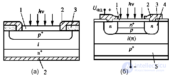 Fig. 5
Fig. 5a and 5b schematically show the design of a p-i-n photodiode and an avalanche photodiode, respectively. Where: 1. — anti-reflection coating; 2. — metal contacts; 3. — silicon oxide SiO2; 4. — guard ring; 5. — substrate.
To reduce reflection of light from the diode surface, it is coated with film 1. A guard ring 2 is formed around the perimeter of the working surface, which allows increasing the breakdown voltage. Optimally chosen dimensions of the device elements make it possible to obtain very good parameters. At a voltage of 100...150 V, the speed of an avalanche photodiode turns out to be approximately 0.3 ns.
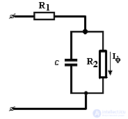 Fig. 6
Fig. 6 shows the equivalent circuit of a photodiode, where R1 is the series resistance modeling the base resistance, C is the capacitance of the p–n junction, and R2 is the internal resistance of the p–n junction. Speed is limited by the transit time of photoexcited carriers and the time constant t=R1C(1+R1/R2). The transit time of carriers at a velocity of 10^7 cm/s and a depleted layer width of 100 μm is about 1 ns. With a smaller depleted layer width, a cutoff frequency of up to several gigahertz can be achieved. The diode capacitance is 1...2 pF (the sum of the package's stray capacitance and the junction capacitance). If the load resistance is taken to be 50 Ω, then the time constant t=0.05...0.1 ns.
Dark current is the leakage current, which increases as the reverse bias voltage increases. When operating in photodiode mode, higher dark current values are observed, which depend on ambient temperature.
As the temperature rises by 10 °C, the dark current increases by approximately a factor of 2, while the shunt resistance halves for every 6 °C rise in temperature. The higher the bias voltage, the smaller the junction capacitance, but the larger the dark current.
Dark current also depends on the semiconductor material and the size of the active area. For example, silicon photodiodes have significantly lower dark current values than germanium ones. The table below shows various semiconductor materials and their relative values of dark current, sensitivity, speed, and cost.
|
Material |
Dark current |
Speed |
Spectral range |
Cost |
|
Silicon (Si) |
Low |
High |
Visible – Near IR |
Low |
|
Germanium (Ge) |
High |
Low |
Near IR |
Low |
|
Gallium phosphide (GaP) |
Low |
High |
UV - Visible |
Medium |
|
Indium gallium arsenide (InGaAs) |
Low |
High |
Near IR |
Medium |
|
Indium arsenide antimonide (InAsSb) |
High |
Low |
Near – Mid IR |
High |
|
Mercury cadmium telluride (MCT, HgCdTe) |
High |
Low |
Near – Mid IR |
High |
Dark current (which flows through the diode regardless of the photocurrent) is the sum of the reverse current and the surface leakage current. It gives rise to shot noise. In silicon photodiodes, the dark current is small (about 10^-12 A), so the noise level is relatively low. The noise characteristics of germanium devices are noticeably worse.
If the power of the incident radiation is P0, then the corresponding number of incident photons will be P0/hν and the photocurrent
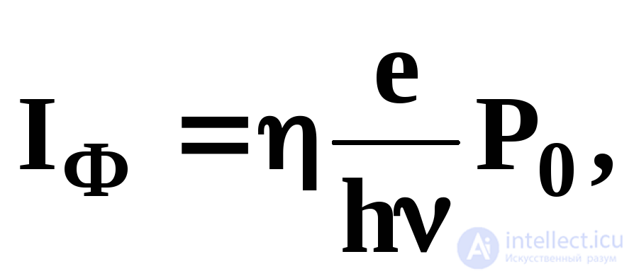 (5)
(5)
where  is the quantum yield, e is the electron charge, h is Planck's constant,
  is the frequency.
The quantum yield is then determined by the relationship:
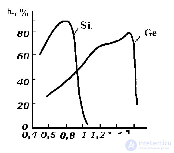 Fig. 7
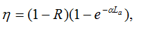 (6)
(6)
where R is the reflection coefficient of the flux from the device's working surface; La is the width of the light absorption region;  is the absorption coefficient
Fig. 7 shows the dependence of quantum yield on radiation wavelength for germanium and silicon. The sensitivity boundary in the long-wavelength region is determined by the material's bandgap width, while the drop in sensitivity in the short-wavelength region is due to a decrease in the absorption length near the surface and surface recombination of photoexcited carriers. The design and connection circuit of a photodiode are shown in Fig. 8a, b, where: a — design, b — connection circuit of the photodiode. Plate 1 made of single-crystal germanium with n-type conductivity is secured with a crystal holder 2 in a kovar package 3. This plate serves as the base of the photosensitive element and is positioned opposite the window, which is closed by a glass converging lens 10. The p-n junction is formed by fusing a drop of indium 8 into the germanium plate — an alloy junction. When indium is fused with germanium, diffusion of indium into the adjacent region of germanium creates a layer with p-type conductivity. Lead 4 from the indium electrode is routed through a kovar tube 5, secured by a glass insulator 6 in the package's stem 7. The other electrode is the photodiode's case, since the germanium crystal is soldered to the crystal holder with a tin ring 9. To protect the p-n junction from environmental effects, the photodiode case is hermetically sealed. Photodiodes based on germanium and silicon are the most widespread. Semiconductor compounds of elements from groups AIIIBV and AIIBVI (GaAs, InAs, InSb, InP, CdS, CdTe, HgCdTe, etc.) are also used. Photodiodes are used as receivers of laser beams in sound-reproducing equipment.
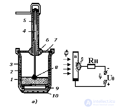 Fig. 8
The main difference from a p-i-n photodiode is that in the base of a p-n photodiode, only diffusion processes occur, not drift processes. Hence the greater inertia and lower carrier collection efficiency at significant base thickness, i.e. when working with IR radiation.
At λ > 0.85…0.90 μm, the photosensitivity of a p-n photodiode is an order of magnitude lower than that of a p-i-n photodiode.
But p-n photodiodes also have important advantages.
They are simpler to manufacture, and the use of a low-resistivity, homogeneous starting semiconductor wafer results in increased uniformity of parameters. This is especially important when creating multi-element, matrix photodetectors.
In the short-wavelength region (λ < 0.55 μm), the differences in carrier collection between p-n and p-i-n structures disappear. The main and extremely important advantage of silicon p-n photodiodes lies in the complete compatibility of their manufacturing technology with integrated-circuit technology, and their low cost.
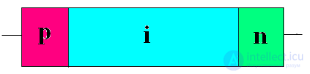
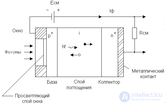
A p-i-n photodiode is a type of photodiode in which an intrinsic (undoped) semiconductor (i-region) is located between the electron (n) and hole (p) conductivity regions. The thickness of the i-layer is chosen to be quite large (500–700 μm), and the doped layers are made very thin so that all the optical radiation is absorbed in the i-layer and the time for transferring charges from the i-region to the doped regions is reduced.
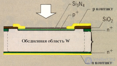
Design of a pin photodiode
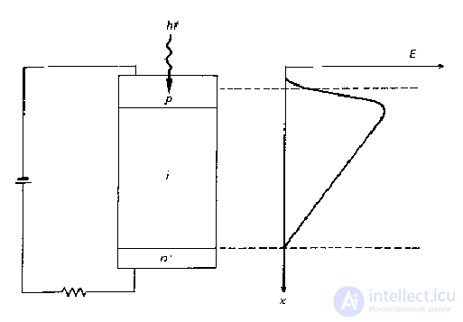
Operating principle of a p-i-n photodiode
A photon enters the i-region, generating electron-hole pairs. The charge carriers, entering the electric field of the space-charge region, begin to move toward the heavily doped regions, creating an electric current that can be detected by an external circuit. The diode's conductivity depends on the wavelength, intensity, and modulation frequency of the incident radiation. The i-layer is called the depleted layer, since it contains no free carriers. Heavy doping of the outer layers makes them conductive, so the entire voltage drop occurs across the i-layer, and the maximum electric field value is created in it.
Main parameters: sensitivity (in modern p-i-n photodiodes, sensitivity ranges from 10 nW to 100 pW, corresponding to -50 dBm); quantum efficiency (in p-i-n photodiodes it usually reaches 80%; for photodiodes designed for use in fiber-optic lines, the junction capacitance equals 0.2 pF at a diode working surface of 200 μm); response time (photogenerated carriers in the i-layer will be separated by the strong electric field, and the photoresponse of such diodes will be fast).
Silicon p-i-n photodiodes
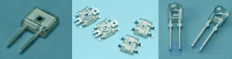
Silicon p-i-n photodiodes have low charge capacitance, which allows them to operate over a wide range of frequencies at low bias voltage. When silicon p-i-n photodiodes are connected to a high-speed preamplifier, their small total capacitance provides high speed and low noise. This feature makes silicon p-i-n photodiodes ideal detectors for use in high-speed photometry and optical communication lines. These devices come in several package types (metal, ceramic, and plastic) and with various active-area sizes. p-i-n photodiodes with micro-lenses are also available, which increase the optical power transfer coefficient.
Advantages:
Disadvantages:
Connection circuit of a p-i-n photodiode
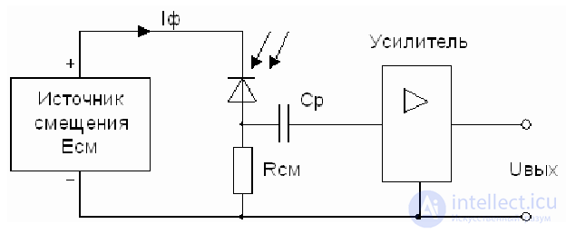
In this connection circuit, the coupling capacitor Cp makes it possible to eliminate the high bias voltage of up to 30 V from the input of the low-noise amplifier. The dynamic range of input optical powers for the photodiode circuit with amplifier can reach 60 dB.
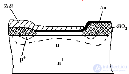
A metal-semiconductor contact, or Schottky barrier, is the equivalent of a p-i-n photodiode in the short-wavelength region of the spectrum, when all radiation is absorbed in the space-charge region. For λ≈0.63 μm (orange-red spectrum), produced by a helium-neon laser, at a speed of ≈10-10s, the theoretical limit of photosensitivity Sph≈0.5 A/W is almost reached. A film of high-resistivity pure Si is grown on a heavily doped n+ silicon substrate. Then, after forming p+-type diffusion rings, a very thin ≈0.01 μm metal film (Au, Al, Mo, etc.) is deposited on a carefully cleaned Si surface, with anti-reflection coatings of SiO2 and ZnS applied on top. The metal film provides significantly lower series resistance than an ordinary p+-n junction, and parasitic absorption of short-wavelength radiation in the metal film is also lower than in the p+ region, due to the sharp difference in thicknesses. This is the decisive advantage of a Schottky-barrier photodiode compared with p-n (or p-i-n) structures in the short-wavelength region of the spectrum.
Additional advantages of these devices stem from the possibility of their simple manufacture using low-temperature technology on a wide variety of semiconductors, even ones in which it is not possible to obtain p-n junctions.
Schottky-barrier photodiodes have technological and physical compatibility with integrated-optics structures.
Heterophotodiodes. Two regions can be distinguished in the design of a heterophotodiode (HPD): a wide-gap window and an active photosensitive layer. The wide-gap window transmits radiation into the active region without significant losses and at the same time serves as a contact layer with low series resistance.
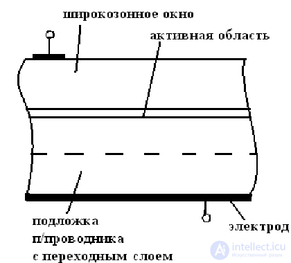
The processes in the active region — absorption of radiation, accumulation of generated charge carriers — proceed in the same way as in a silicon p-i-n structure. The difference is that, by choosing a suitable semiconductor compound for the photosensitive layer, complete absorption of radiation can be achieved with this layer only about 1 μm thick. Hence the combination of high speed and high photosensitivity at low supply voltages, which is fundamentally unattainable for Si p-i-n structures in the long-wavelength IR region. For such a structure at λ≈1.06 μm, the thickness of the i-region must be about 300 μm, and the operating voltage hundreds of volts.
Thus, HPDs are in some sense the equivalent of silicon p-i-n diodes in the long-wavelength region. An extremely important advantage of HPDs is also their physical and technological compatibility with integrated-optics devices. For example, this opens up the possibility of creating universal monolithic optoelectronic elements for duplex (two-way) communication.
HPDs are significantly more complex to manufacture and have an increased noise level.
Freedom in choosing the HPD material also makes it possible to achieve increased photo-EMF values (for example, Uoc=0.8…1.1 V for GaAlAs structures), a high conversion efficiency (≈100%), lower dark currents and noise than in silicon photodiodes, an extended temperature range, and increased resistance to penetrating radiation.
MOS photodiode, or photosensitive MOS structure, is used in various electrical modes. One such capability is characteristic of CCDs, where radiation is converted into a charge of minority carriers, which accumulates at the semiconductor-dielectric interface and, when needed, is read out (transferred along the surface) via the charge-coupling mechanism. This same charge modulates the conductivity of the near-surface region (MOS channel), which leads to a change in the output signal of the MOS transistor or the resistance of the MOS photoresistor. Charge exchange between the semiconductor and the dielectric causes polarization of the dielectric, which persists for a long time after the radiation stops, i.e. a "memorization" of the light signal occurs. Under optical or electrical influences, the recorded information can be read out using appropriate methods.
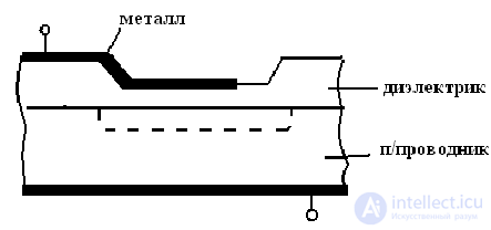
Special MOS structures with a very thin "tunnel-transparent" dielectric pass electric current and have properties close to those of Schottky-barrier photodiodes. Such an MOS photodiode generates current signals in exactly the same way as any other photodiode.
The concept of the dynamic mode also gave rise to an even more unusual MOSOM photodiode, in which photocarriers generated in the semiconductor (usually close to intrinsic) are spatially stretched under the applied voltage but do not leave the crystal, and can only recombine. This makes it possible to obtain a significant amplification of the photocurrent, similar to what happens in photoresistors.
MOS structures make it possible to achieve very high multiplication factors (up to M≈105, compared with ≈102…103 for ordinary APDs) and to create large, uniform photosensitive areas (up to several cm2).
Manufacturing a high-quality MOS structure is significantly more difficult than a p-n junction, since a p-n junction is created inside a single crystal, whereas in an MOS element structurally and chemically dissimilar materials interact.
Advantages of MOS photodiodes.
Functional versatility. The equivalent of optical information in them can be: electric charge, change in channel conductivity, dielectric polarization, photo-EMF, photocapacitance, or continuous or pulsed photocurrent;
Design and process flexibility, i.e. the ability to vary the range of semiconductors, dielectrics, and metals, the "low-temperature" nature of most process steps, and the use of monoplanar and thin-film polycrystalline structures;
High values of photoelectric parameters, and the ability to vary them over a wide range. MOS photodiodes can operate both in the short-wavelength region (like Schottky-barrier photodiodes) and in the long-wavelength region (like p-i-n structures); the presence of a dielectric allows minimal dark currents to be obtained (and, as a result, low noise);
Physical, electrical, and technological compatibility with bipolar, and especially with MOS, integrated circuits.
A metal-semiconductor structure. When the structure is formed, part of the electrons will transfer from the metal into the p-type semiconductor.
The structure makes use of avalanche breakdown. It occurs when the energy of the photocarriers exceeds the energy required to generate electron-hole pairs. Very sensitive. To evaluate it, there is an avalanche multiplication coefficient:

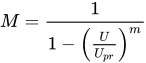
To achieve avalanche multiplication, two conditions must be met:
1) The electric field of the space-charge region must be large enough that, over the mean free path, an electron gains energy greater than the bandgap width:

2) The width of the space-charge region must be substantially greater than the mean free path:

The internal gain coefficient value is M = 10—100, depending on the type of photodiode.
A heterojunction is a layer that arises at the boundary of two semiconductors with different bandgap widths. One p+ layer plays the role of a "receiving window." Charges are generated in the central region. By selecting semiconductors with different bandgap widths, the entire wavelength range can be covered. The drawback is the complexity of manufacture.
When radiation quanta act on the base, free carriers are generated there and move toward the boundary of the p-n junction. The width of the base (n-region) is made such that the holes do not have time to recombine before crossing into the p-region. The photodiode current is determined by the current of minority carriers — the drift current. The speed of the photodiode is determined by the rate at which the p-n junction's field separates the carriers, and by the capacitance of the p-n junction Cp-n
The photodiode can operate in two modes:
Features:
-
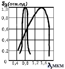
Fig. 2
current sensitivity Si (A/lm or A/W) — determines the value of the photocurrent produced by a unit flux of radiation; the static integral current sensitivity for a monochromatic light flux or radiant power is determined by the ratio:
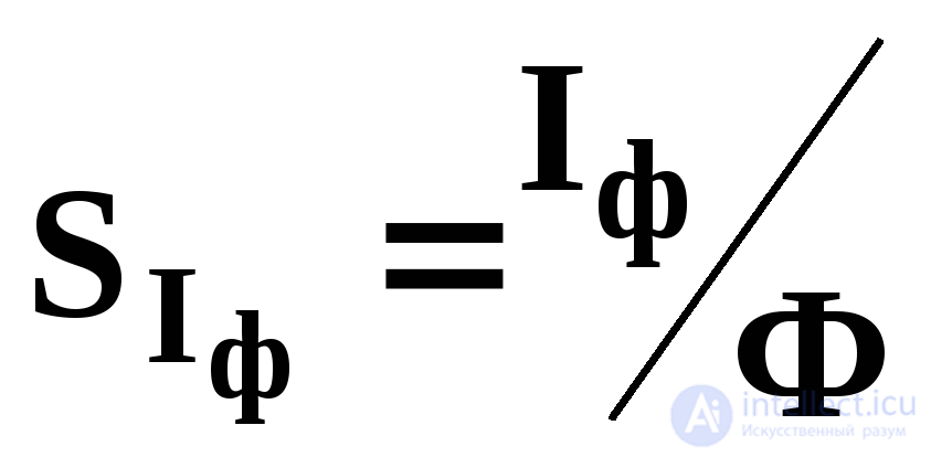 (1)
(1)
or
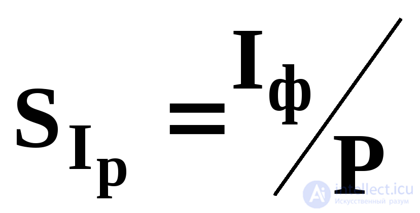 (mA·W-1) (2)
where Iph is the photocurrent; Φ is the light flux, P is the radiant power.
When the device operates in photodiode mode, it is convenient to use the concept of integral voltage sensitivity:
 (3)
(3)
 (4)
(4)
where UOUT is the change in output voltage; RL is the load resistance.
- spectral characteristic. Shows the distribution of the material's sensitivity with respect to the wavelength of the radiation incident on it. Fig. 2 shows typical spectral characteristics of silicon (2) and germanium (1) photodiodes. As can be seen from Fig. 2, the sensitivity maximum of germanium diodes is shifted toward longer wavelengths.
- rise time constant  and fall time constant
  of the photocurrent; they determine the limiting values of the light-flux modulation frequency at which a decrease in photoresponse is not yet noticeable. These parameters characterize the inertia of the devices. Usually
  .
.
- speed — determined by the cutoff frequency fC, corresponding to the maximum light-flux modulation frequency at which the static sensitivity decreases to a level of 0.707 of the sensitivity at low modulation frequency.
- rated operating voltage UNOM, dark current ID and maximum permissible reverse voltage UMAX.
Photodiodes made from silicon operate in the wavelength range of 0.5...1.1 μm. Photodiodes based on germanium operate in the wavelength range of 0.5...1.9 μm.
Most photodiodes are produced in hermetically sealed metal-glass packages. The FD-1 photodiode is produced in a metal-ceramic package, and the FD-2 photodiode in a plastic package. The positive lead of photodiodes is marked on the package with a "+" sign, a dot, or a colored mark at the lead-in. To let optical radiation into the photosensitive element, input windows, lenses, light guides, and other optical elements are built into the photodiode package. The FD-20-30K photodiode is produced without a built-in input optical element. The FD20-32K and FD-20-30K photodiodes each have two photosensitive elements, the FD-19K, FD-20KP, and FD-22KP have three, and the FD-20-33K has four. The FD-246 photodiode has 64 photosensitive elements. The FD-K-142 photodiode has a position-sensitive, square, four-element optical input.
Advantages of photodiodes:
Disadvantages of photodiodes:
P-n photodiodes are used in applications similar to those of other photodetectors, such as photoconductors, charge-coupled devices, and photomultipliers. They can be used to generate an output signal that depends on illumination (analog; for measurement, etc.), or to change the state of a circuit (digital; either for control and switching, or for digital signal processing).
Photodiodes are used in consumer electronics devices such as compact-disc players, smoke detectors, medical instruments [16], and receivers for infrared remote-control devices used to control equipment ranging from televisions to air conditioners. For many applications, either photodiodes or photoresistors can be used. Any type of photosensor can be used to measure illumination, for example in camera light meters, or to respond to light levels, for example when turning on street lighting after dark.
Photosensors of all types can be used to respond to incident light or to a light source that is part of the same circuit or system. A photodiode is often combined into a single component with a light emitter, usually an LED, either to detect the presence of a mechanical obstruction to the beam (a slotted optical switch), or to connect two digital or analog circuits while maintaining extremely high electrical isolation between them, often for safety purposes (an optocoupler). A combination of LEDs and photodiodes is also used in many sensor systems to characterize various types of products based on their optical absorption.
Photodiodes are often used for precise measurement of light intensity in science and industry. They generally have a more linear response than photoconductors.
They are also widely used in various medical applications, such as detectors for computed tomography (combined with scintillators), sample-analysis instruments (immunoassay), and pulse oximeters.
PIN diodes are much faster and more sensitive than p-n junction diodes, and are therefore often used for optical communication and in lighting control.
P-n photodiodes are not used to measure very low light intensity. Instead, if high sensitivity is required, avalanche photodiodes, intensified charge-coupled devices, or photomultipliers are used for applications such as astronomy, spectroscopy, night-vision instruments, and laser rangefinding.
Photodiodes are basic elements of many optoelectronic devices.
A photodiode can offer significant operating speed, but its current gain does not exceed unity. Thanks to optical coupling, such chips have substantial advantages: ideal galvanic isolation of the control circuits from the high-power circuits. At the same time, a functional connection between them is preserved.
These devices, in the form of photodiode arrays and scanistors, are new, advanced electronic devices. Their optoelectronic eye with a photodiode can generate a response to the spatial and brightness properties of objects. In other words, it can perceive the object's complete visual image.
The number of light-sensitive cells is very large. Therefore, in addition to questions of speed and sensitivity, reading out the information is also necessary.
All photodetectors with multiple photoelements are scanning systems, that is, devices that allow the area under study to be analyzed through sequential, element-by-element viewing.
Photodiodes have also found wide application in fiber-optic lines and laser rangefinders. Recently, such photodiodes have also come to be used in positron emission tomography.
At present, samples of photosensitive arrays composed of avalanche photodiodes exist. Their efficiency and range of application depend on a number of factors.

Comments