
Lecture
INTRODUCTION
Electronics is a branch of science and engineering that studies: physical phenomena in semiconductor devices; the electrical characteristics and parameters of semiconductor devices; and the properties of devices and systems based on the use of semiconductor devices.
Electrical conductivity of semiconductors
Semiconductor devices are manufactured from simple semiconductor materials - germanium Ge, silicon Si, selenium Se - and compound semiconductor materials - gallium arsenide GaAs, gallium phosphide GaP, and others.
In pure semiconductors the concentration of charge carriers - free electrons and holes - is low. Therefore, to give a semiconductor a specific type of conductivity, certain impurities are introduced into it. This process is called doping.
p-type semiconductor
The main charge carriers are holes.
Group III elements (Al, Ga) create hole conductivity.
n-type semiconductor
The main charge carrier is the electron.
Group V elements (vanadium V, niobium Nb) create electron conductivity.
An electron-hole junction, or p-n junction, is the region at the boundary between two semiconductors, one of which has electron conductivity and the other hole conductivity.
Component base of modern electronic devices
Classification of semiconductor devices
Semiconductor devices are devices whose operation is based on the properties of the p-n junction
1. Resistors
2. Diodes
3. Transistors (BJT, FET, IGBT)
4. Thyristors
5. Integrated circuits
Semiconductor resistors
A semiconductor resistor is a two-terminal semiconductor device that makes use of the dependence of a semiconductor's electrical resistance on voltage, temperature, illumination, and other controlling parameters.
Linear
A semiconductor resistor employing a lightly doped material such as silicon or gallium arsenide. The resistivity depends only slightly on the electric field strength => the resistance is approximately constant over a wide range of U and I. Used in integrated circuits.
Nonlinear
A varistor is a semiconductor resistor whose resistance depends on the applied voltage and whose I-V curve is nonlinear.
Thermistor (temperature-dependent resistor) - a semiconductor resistor that makes use of the dependence of a semiconductor's electrical resistance on temperature.
• NTC thermistor: R↓ as t°↑
• PTC thermistor (posistor): R↑ as t°↑
Photoresistor - a semiconductor resistor whose resistance depends on illumination.
Strain gauge - a semiconductor resistor whose resistance depends on mechanical deformation.
Diodes
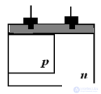
Semiconductor diodes are semiconductor devices with a single p-n junction and two terminals.
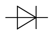
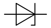
Classification of semiconductor diodes and their symbols
Designation system
1 - source material:
germanium - letter G or digit 1;
silicon - letter K or digit 2;
gallium - letter A or digit 3;
indium - letter I or digit 4
2 - device type:
A - microwave diodes
B - varicaps
D - rectifier and pulse diodes
I - tunnel diodes
L - light-emitting diodes (LEDs)
N - diode thyristors (dinistors)
S - Zener diodes
Ts - rectifier stacks and assemblies
3 - digits indicating certain basic parameters of the diode (power) (for Zener diodes the fourth element characterizes the stabilization voltage),
4 - letters and/or digits indicating the design serial number
5 - a letter defining the classification by parameters.
Planar rectifier diodes
Zener diode
Tunnel diodes

Varicaps

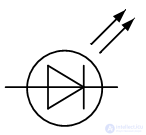
LEDs
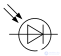
Photodiodes
Point-contact diodes
Low-power
Rectifier
Microwave diodes
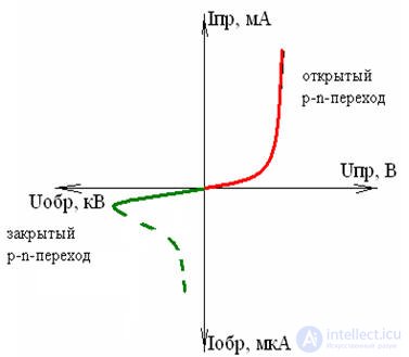
Current-voltage characteristic (I-V curve) of a real diode
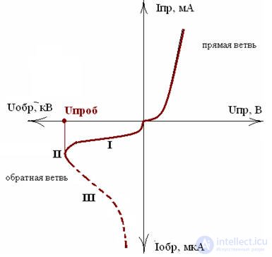
For engineering purposes the I-V curve is used in linear coordinates.
At high reverse-bias voltages, breakdown may develop in the diode - a sharp increase in reverse current with only a slight change in voltage. In avalanche breakdown, electrons in the electric field of the p-n junction acquire energy sufficient to ionize the semiconductor's own atoms. This leads to an avalanche multiplication of charge carriers, a sharp increase in their local concentration, and correspondingly of the current. After avalanche breakdown develops, the diode does not lose its functionality. This type of breakdown is used in semiconductor Zener diodes, whose properties will be discussed further below.
Thermal breakdown develops as a result of local heating of the p-n junction region and, as a consequence, an increase in charge carrier concentration. Thermal breakdown is irreversible, after which the diode loses its properties and functionality.
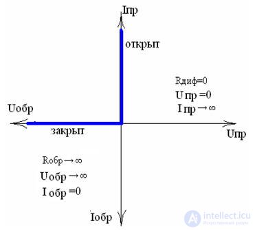
Current-voltage characteristic of an ideal diode
Main diode parameters
The parameter system is given in reference manuals. This system allows the correct selection of a diode for use under specific conditions.
Ifwd - forward current, flowing in the forward direction,
Ufwd - forward voltage,
Ifwd max - maximum available forward current,
Urev max - maximum available reverse voltage,
Irev - diode reverse current,
Urev - diode reverse voltage - (constant voltage applied to the diode in the reverse direction).
Example: KD204A Ifwd = 2 A, Urev max = 400 V,
Ufwd = 1.4 V, Irev = 150 µA
Diodes, as nonlinear elements, are characterized by
static resistance Rs = U/I
differential (dynamic) resistance Rdiff = ∆U/∆I
Zener diodes
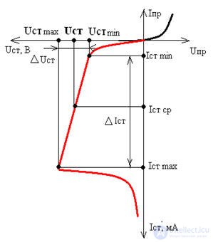
A Zener diode is a semiconductor diode whose voltage in the electrical breakdown region under reverse bias depends only weakly on the current within a specified range, and which is intended for stabilizing the voltage level in a circuit.
Actual I-V curve of a Zener diode
Ideal I-V curve of a Zener diode
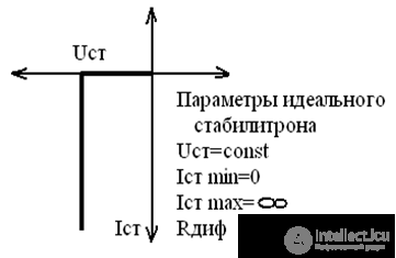
Main parameters
1. Ust (stabilization voltage)
2. Differential resistance Rdiff = 0.5 - 200 Ohm
3. Ist min - minimum stabilization current
4. Ist max - maximum stabilization current
Imax ≈ Pmax/Ust
Silicon diodes, which have high resistance to thermal breakdown, are used as Zener diodes.
Silicon Zener diodes are used to stabilize power supply voltages, as well as to fix voltage levels in various circuits.
Groups of low-power diodes in the form of diode matrices and diode arrays are used in logic devices, decoders, and other computing-technology elements.
A Zener diode is usually connected in a stabilization circuit so that its p-n junction is reverse-biased.
For stabilizing low voltages U = 1 - 1.5 V, voltage limiter diodes (stabistors) are used
Structural elements of integrated circuits
Package - the part of an IC's construction intended to protect the microcircuit from external influences and to connect it to external electrical circuits by means of leads.
Substrate - a dielectric blank intended for depositing elements, interconnections, and contact pads onto it.
Board - part of the substrate, or the entire substrate, on the surface of which film elements of the microcircuit, interconnections, and contact pads are formed.
Semiconductor wafer - a blank of semiconductor material intended for manufacturing an IC;
Die (chip) - part of the wafer, in the volume and on the surface of which the elements of the semiconductor microcircuit, interconnections, and contact pads are formed;
Contact pad - a metallized area on the board, die, or IC package, used for connecting the leads of components and dies, jumpers, and also for monitoring its electrical parameters and operating modes;
Chip-scale (unpackaged) IC - a microcircuit die intended for mounting in a hybrid IC or micro-assembly;
Lead - a conductor electrically connected to the die's contact pad and mechanically attached to its surface to provide electrical contact with external circuits.
Main IC parameters
Packing density - the quantity per unit volume
Integration level - the number of elements comprising the IC per 1 cm3
1st integration level - up to 10 elements/cm3
2nd integration level - 10-100 elements/cm3
3rd integration level - 100-1000 elements/cm3
4th integration level - up to 100,000 elements/cm3
etc.
Classification of ICs by manufacturing technology
Semiconductor - All microcircuit elements are produced in a single technological cycle; all elements are formed within the volume and on the surface of a semiconductor die. Semiconductor ICs consume 50-200 mW.
Hybrid - a microcircuit that, in addition to elements, contains simple and complex components (several semiconductor ICs). Passive elements are formed by depositing various films onto the surface of a dielectric substrate made of glass, ceramic, glass-ceramic, or sapphire, while the active elements are unpackaged semiconductor devices.
Film - a microcircuit in which all elements and interconnections are formed only as films of conducting and dielectric materials
Secondary Power Supply Source
An SPS (secondary power supply) is an electronic device intended to convert an alternating voltage into a direct voltage of the required value.
To obtain electrical energy of the required type, it is necessary to convert AC energy into DC energy using rectifiers, and DC energy into AC energy using inverters.
Rectifiers and inverters are secondary power supply sources.
Let us consider a secondary power supply source that converts AC energy into DC energy. Such secondary power supply sources (SPS) are needed for powering various pieces of electronic equipment (DC motors, various amplifiers, chargers, etc.).
Rectification is the process of converting alternating current into direct current using rectifying devices that have one-way conductivity. Rectifying devices consist of the following main units: a transformer, an electric valve (rectifying element), a smoothing filter, and a voltage regulator.
Modern electronic semiconductor devices in discrete and, especially, microelectronic form impose very strict requirements on the quality of the consumed power, which must be highly stable
Classification of secondary power supplies
1. Uncontrolled (diode-based), controlled (thyristor-based).
2. By the number of phases of the supply AC voltage: single-phase, three-phase
3. By the shape of the rectified voltage: half-wave, full-wave (bridge, or with a transformer center tap).
Single-phase low-power rectifying devices are used to power DC loads with power from 1 W to 1 kW. Accordingly, such a power source is called a low-power secondary power supply (LPSPS).
Let us consider the block diagram of an LPSPS device, Fig. 1.
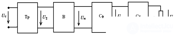
Fig. 1. Block diagram of an LPSPS
Description of the operation of the main LPSPS units
At the input, the transformer (Tr) changes the AC voltage Us to the required value U2, that is, it matches the input voltage to the load and provides electrical isolation between the source of rectified voltage and the load device.
After the transformer comes the diode valve group (V), where U2 is converted into a pulsating voltage Up. The number of valves depends on the rectifier circuit.
In the rectified voltage Up, besides the constant component, there is also an alternating component, which is reduced to the required level U by the smoothing filter (Sf) and has very small ripple.
The voltage regulator (R) keeps the voltage Uload constant across the load device Rload.
Depending on operating conditions, some units may be absent (the transformer or the regulator).
Two types of rectifiers are used to rectify single-phase alternating voltage: half-wave and full-wave
Half-wave rectifier
It is assumed that the transformer and rectifying diode are ideal, i.e., the transformer's winding resistance is zero, and for the diode Rfwd = 0 and Rrev = ∞.
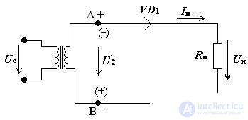
Fig. 2 Half-wave rectifier circuit
Principle of operation of the rectifier
Let us consider the timing diagrams of the half-wave rectifier (Fig. 3): in the time interval 0 - T/2 diode VD1 is open, φA > φB, and current iload flows in the load.
In the time interval T/2 - T the diode is closed, φA < φB, and U2m is applied across the diode.
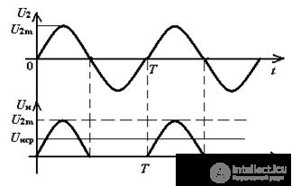
Fig. 3. Timing diagrams of the half-wave rectifier
The current and voltage in the load are pulsating in nature and consequently differ significantly from their constant components
Main electrical parameters of a rectifier
The diode is the main element in rectifiers and largely determines the rectifier's main performance figures.
1. Uload avg and Iload avg - average values of the rectified voltage and current in the load device
2. Load device power Pload avg = Uload avg • Iload avg
3. Amplitude of the fundamental harmonic Ufund
4. Ripple factor of the rectified voltage
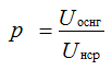
5. Rectifier efficiency
6. Maximum reverse voltage on the blocked diode Urev max
Let us determine the average value of the rectified voltage and current in the load.
In a half-wave rectifier, more than half of the input voltage is lost!

Input voltage (voltage on the transformer's secondary winding):
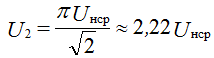
Average value of the rectified current; the average rectified current equals the current through the diode:
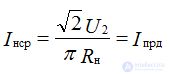
The ripple frequency of the rectified voltage equals the frequency of the mains voltage:
fp = ffund
The rectified voltage has a non-sinusoidal waveform, so it can be expanded into a Fourier series:

Since the ripple frequency of the rectified voltage equals the mains frequency, the voltage of the fundamental (first) harmonic is used when calculating the ripple factor:
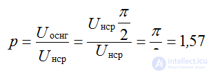
p = 1.57 - a very large ripple factor - this is a drawback of the circuit.
The maximum reverse voltage on the blocked diode equals the amplitude of the input voltage:
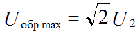
When selecting rectifier diodes, the maximum allowable parameters are used: the maximum allowable forward current and the maximum allowable reverse voltage: Ifwd max, Urev max.
The diode is the main element in rectifiers, and its parameters largely determine the rectifier's main parameters
Full-wave bridge rectifier
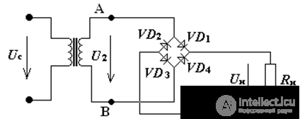
Fig. 1 Full-wave bridge rectifier
Principle of operation of the bridge rectifier
The diode bridge circuit is connected to the secondary winding of the transformer, Fig. 1;
each pair of diodes operates in turn, VD1-VD3 and VD2-VD4: on the timing diagrams, Fig. 2,
in the time interval 0-T/2, VD1-VD3 are open and VD2-VD4 are closed; current Iload flows in the load;
in the time interval T/2-T, VD1-VD3 are closed and VD2-VD4 are open; current Iload flows in the load;
the ripple frequency of the rectified voltage is twice the mains frequency
fp = 2fs = 100 Hz.
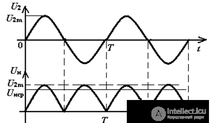
Fig. 2. Timing diagrams of the bridge rectifier
Main parameters of the bridge rectifier
1. Average rectified voltage:
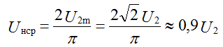
2. Average rectified current:
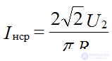
Diode forward current:
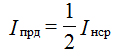
3. Expanding the voltage across the load into a Fourier series, we obtain the numerical value of the ripple factor for the bridge rectifier circuit:

Amplitude of the fundamental second harmonic at frequency 2ω:
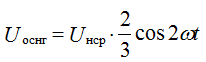
Consequently, the ripple factor will equal:
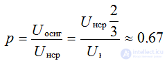
The maximum reverse voltage on each of the closed diodes has the same value as in the half-wave rectifier, since with respect to the input they are connected in parallel:
U2m = √2 U2;
Urev max = π•Uload avg; Urev max = √2 U2
The main drawback is the large number of diodes.
Semiconductor rectifier bridge assemblies (KTs402, KTs403, and others) are currently manufactured
Smoothing filters
The output of a rectifier is a pulsating DC voltage. For many electronic devices the ripple factor of the supply voltage must not exceed p = 10^-2 - 10^-5. Therefore, smoothing filters are used to reduce the ripple.
Filters are usually built from reactive elements: capacitors and inductors (chokes). The reactive properties of these elements are used here: connected in series, an inductor has high impedance to alternating current; connected in parallel, a capacitor has low impedance to alternating current. A characteristic feature of filters is that a capacitive filter smooths ripple better at low load currents, while an inductive filter, conversely, does so better at high currents.
A capacitive filter is always connected in parallel with the load. Let us consider a half-wave rectifier with a smoothing capacitive filter, Fig. 3.
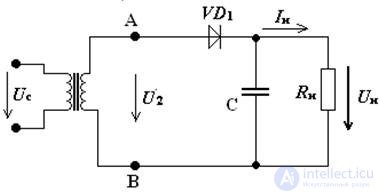
Fig. 3 Half-wave rectifier circuit with a capacitive filter
The smoothing principle can be described as follows (Fig. 4), for the circuit of Fig. 3: during the first half-cycle (0 - T/2), when the potential of point A is higher than that of point B, diode VD1 is open and the capacitor charges through the diode's low internal resistance up to U2max. When the potential of point A falls below the voltage on the capacitor, during the second half-cycle (T/2 - T) the diode is closed and the capacitor discharges through the load resistor Rload, until the potential of point A again exceeds the voltage on the capacitor.
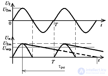
Fig. 4 Timing diagrams of the voltage of a half-wave rectifier with a capacitive filter
The voltage across the blocked diode will be determined by Kirchhoff's second law:
Urev max = Uc + U2max
and since the capacitor charges up to the value U2max, it follows that:
for a half-wave rectifier:
Urev max = 2•U2max = 2√2 U2
for a full-wave rectifier:
Urev max = U2max = √2 U2
The average rectified voltage of rectifiers with a filter is determined by the formula
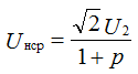
Full-wave bridge rectifier with a smoothing capacitive filter
Let us consider a full-wave bridge rectifier with a smoothing capacitive filter, Fig. 5.
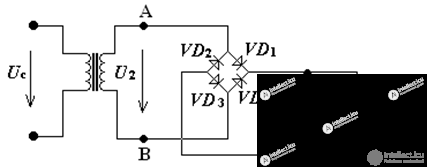
Fig. 5 Bridge rectifier circuit with a capacitive filter
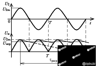
Fig. 6 Timing diagrams of the bridge rectifier with a capacitive filter
From analysis of the timing diagrams (Fig. 4, Fig. 6) it is evident that as the capacitance C changes, the ripple factor of the rectified voltage changes as well. The less the capacitor discharges, the smaller the ripple in the rectified current Iload will be.
The discharge time constant of the capacitor: τdis = C•Rload.
If τdis >> T, the ripple factor is calculated using the formulas:
for the half-wave circuit:
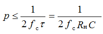
where: fs is the mains voltage frequency;
for the full-wave circuit:
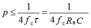
where: fs is the mains voltage frequency.
To select a capacitor it is necessary to calculate its capacitance and working voltage.
For small ripple, the filter capacitance is determined by the formula:
for a half-wave rectifier
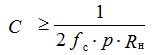
for a full-wave rectifier
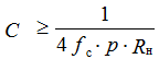
The capacitor's rated working voltage is calculated with a 30% margin and equals:
Uwork ≥ 1.3∙U2max
It must be taken into account that manufactured capacitors have a capacitance tolerance of ±12% of the nominal value.
The main parameter characterizing the effectiveness of an electrical smoothing filter is the smoothing coefficient, equal to the ratio of the ripple factors at the filter's input and output. When designing filters, the following requirements must be met: minimal voltage drop across the filter elements, and minimal size and weight.
When using a capacitive filter, it must be taken into account that the maximum value of the current through the diode is determined only by this element's internal resistance, and therefore it can reach values exceeding the maximum allowable forward current of the diode. Such a current can damage the diode. To avoid this, an additional resistor is connected in series with the diode.
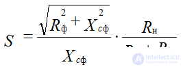
If a higher smoothing coefficient is required, more complex LC or RC filters are used. Connecting an inductor to a capacitive filter results in the voltage drop across the inductor significantly reducing the share of the alternating component of the rectified voltage, while the voltage drop from the constant component is nearly zero. The only problem when using an inductor is that it increases the mass and dimensions of the LPSPS. Therefore, in an LPSPS, a resistor Rf is used instead of an inductor Lf. The filtering action of Rf consists in the fact that when Xc << Rload, the voltage drop of the alternating component of the rectified voltage across Rf is greater than that of the constant component.
The smoothing coefficient of the filter in this case will equal:
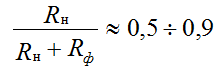
So that the reduction of the constant component is not too large, Rload and Rf are chosen
to be comparable in magnitude:
If a single smoothing filter cannot reduce the ripple of the rectified voltage to the required value, filters are connected in cascade, and the smoothing coefficient is then determined by the formula: S = S1•S2•S3•...Sn
External characteristics of rectifiers
The external characteristic of a rectifier is the dependence of the voltage across the load device on the current through it (Fig. 10).
In a rectifier without a filter (Fig. 7, curve 1), the load voltage and current are related by: 
where Uload,oc is the output voltage of the rectifier in the open-circuit (no-load) mode, i.e., at Rload = ∞,
Rd is the internal resistance of the diode in the open state,
Rtr is the resistance of the transformer winding.
In the rectifier of Fig. 7, curve 1, the no-load output voltage will be Uload,oc; in the rectifier with a filter (Fig. 7, curve 2), the no-load output voltage will be higher, equal to the amplitude value of the input voltage, since with no load, the capacitor charges to the peak value of the voltage on the transformer's secondary winding.
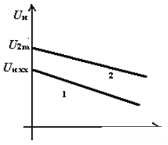
Fig. 7 External characteristics of rectifiers
Three-phase rectifiers
Three-phase AC rectifiers are used as medium- and high-power rectifiers. There are two main types of three-phase rectifiers: the one with a neutral lead and the bridge type.
Three-phase rectifier with a neutral lead
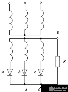
Fig. 1 Circuit of a three-phase rectifier with a neutral lead
Figure 2 shows the timing diagrams of the voltage u2(t) at points a, b, c, and the current through resistor R and diodes VD1, VD2, and VD3.
By Kirchhoff's first law, the current through the resistor equals the sum of the currents of all three branches, taking sign (direction) into account. Since, in this circuit, the currents in each phase are directed toward node d' when the potentials at points a, b, c are positive relative to node d, the total current through the resistor always has the same direction. That is, current rectification takes place.
Let us carry out a more detailed analysis of the three-phase current rectification, Fig. 2.
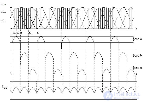
Fig. 2 Timing diagrams of the potentials at points a, b, c - ua(t), ub(t), uc(t); the currents through the diodes iVD1, iVD2, iVD3, and the current through the resistor iR.
At the moment t = 0, the potentials at points a and c are equal. As a result, the potential difference across the terminals of diodes VD1 and VD3 is zero, and therefore the current through these diodes at this moment is zero. The potential at point b is negative relative to the potentials at a and c, so the voltage on diode VD2's terminals is reverse, and no current flows through VD2.
For 0 > t > t1, the potential difference on diodes VD2 and VD3 corresponds to reverse voltage, since ua(t) > uc(t) > ub(t), while on VD1 it is forward. Therefore current begins to flow through VD1 and R, equal to.
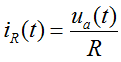
The maximum current through the resistor will be observed at the moment t = t1. At t = t2 the potentials at points a and b become equal and the current through diodes VD1 and VD2 stops due to the potential difference becoming zero. The current through diode VD3 is zero because the potential at point c is negative, and the voltage across it, equal to the potential difference between point c and points a and b, is reverse.
In the intervals from t2 to t3 and from t3 to t4 a similar situation occurs for iVD2 and iVD3. The current through the resistor over time consists of the sequence of currents through diodes VD1, VD2, and VD3.
In a three-phase rectifier with a neutral lead, the ripple factor is p = 0.25.
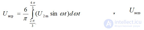
The average value of the rectified voltage and current are given by the following expressions:
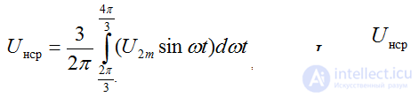
The maximum reverse voltage on the diodes equals the potential difference between the points (a-c)-b, (a-b)-c, and (b-d)-a at the moments t0, t1, 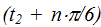 . The potential difference at these moments on diodes VD1, VD2, VD3, respectively, and further, equals:
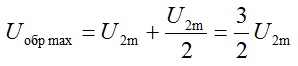
This type of rectifier can provide a rectified current of up to hundreds of amperes, with the rectified voltage reaching several tens of kilovolts. The main drawback is the DC magnetization of the transformer core, which reduces the rectifier's efficiency
Three-phase bridge rectifier
Fig. 3, which in all respects outperforms the three-phase rectifier with a neutral lead. It is used to convert medium- and high-power currents and voltages.
This rectifier contains a bridge of six diodes. During each 1/6 of the period, one pair of diodes is under forward line voltage, while the other four diodes are under reverse voltage.
For example, starting from moment t0 until moment t1, diodes VD1 and VD4 are under forward voltage, since phase a has a positive potential that opens VD1 and closes VD2, while phase b has a negative potential that opens diode VD4 and closes VD3. The potential difference between phases a and b during this period is greater than the potential difference between phases a and c and b and c, so diodes VD2, VD3, VD5, and VD6 are closed and do not conduct current.
In the next time period from t1 to t2, the greatest line voltage occurs between phases a and c. The potential of phase a keeps diode VD1 open and VD2 closed, while the negative potential of phase c opens diode VD6 and closes diode VD5. The remaining diodes are closed because of the smaller potential difference between phases a and b and b and c.
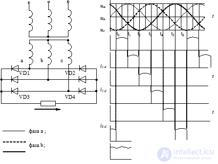
Fig. 3 Three-phase bridge rectifier
and timing diagrams of the rectified voltage and currents.
Next, the following pair of diodes is switched on and the other four are switched off. That is, during the corresponding time periods, the diodes conducting in the forward direction are the ones to which the greatest line voltage is applied.
Clearly, the average values of current and voltage for this rectification circuit are the highest among the circuits considered.
Parametric voltage regulator
In many pieces of radio-electronic equipment that use secondary power supply sources, it is essential to maintain the voltage or current at a certain fixed level, regardless of possible changes in the input voltage and output current. Voltage or current regulators are used to accomplish this task. In this teaching manual we consider a parametric voltage regulator based on a semiconductor Zener diode. Parametric regulators have a simple design and high reliability, but a low efficiency.
The circuit of the parametric voltage regulator, Fig. 4, consists of a ballast resistor Rballast (to limit the current through the Zener diode), and a Zener diode connected in parallel with the load, which performs the main stabilization function.
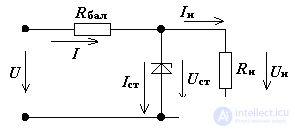
Fig. 4 Circuit of the parametric voltage regulator
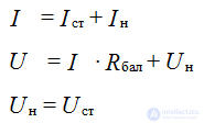
The basic relationships between currents and voltages in the regulator are determined by Kirchhoff's first and second laws:
Operating principle of the parametric regulator
The operating principle of the parametric DC voltage regulator is conveniently explained with the help of Fig. 5, which shows the current-voltage characteristic (I-V curve) of the Zener diode and the "inverted" I-V curve of the ballast resistor. The voltage regulator operates as follows. When the input voltage U of the regulator changes, the current I changes correspondingly, and consequently the currents of the Zener diode and the load change. However, when the Zener diode's current changes, the voltage across it changes by a very small amount, in accordance with the diode's I-V curve (Fig. 5), i.e., it hardly changes at all. According to Kirchhoff's second law, when the input voltage changes, the voltage drop across the ballast resistance changes proportionally to the current and turns out to equal the increment of the input voltage. In other words, the entire increment of the input voltage is dropped across the ballast resistance, while the voltage across the Zener diode and the load hardly changes at all. Let us express the above mathematically:
U ± ∆U = (Ist + Iload ±∆Ist)•Rballast + Uload
Taking U = const and Rload = const, we obtain Iload = const, and the condition for keeping the Zener diode's operating point on segment AB of the I-V curve (Fig. 5) is given by the formula:
±∆U = ±∆Ist•Rballast
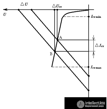
Fig. 5. Explanation of the operating principle of the voltage regulator
It follows from this that normal operation can be ensured by an appropriate choice of the ballast resistance value. Then, when the voltage at the regulator's input changes, the normal limits of stabilization of the output voltage Uload are not violated.
When stabilizing voltage, taking Iload = var, Rload = var, and U = const, at the regulator's input there occurs a redistribution of currents between the load and the Zener diode, while the voltage across the Zener diode and the voltage drop across the ballast resistance remain unchanged, in accordance with the equation:
U = I•Rballast + Uload = ((Iload ± ∆Iload) + (Ist ± ∆Ist))•Rballast + Uload
For normal operation of the regulator under varying load, changes in current must not cause the Zener diode's current to go outside the maximum and minimum allowable values.
Under the condition U = const and Rload = const, the design of the regulator reduces to selecting a Zener diode and choosing the value of Rballast; then, from the system of equations (1), we obtain the formula for calculating Rballast:
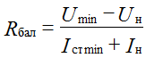
The resistance of the resistor must be such that the Zener diode current is not less than Ist min, i.e., does not go outside the operating segment AB (Fig. 5) of the diode's I-V curve.
The ballast resistance accounts for the main losses of the regulator, so parametric regulators are used only in low-power circuits.
The Zener diode is selected from a reference manual by its parameters:
1. Ist max - the maximum allowable current of the Zener diode;
2. Ust - the stabilization voltage;
3. Ist min - the minimum current of the Zener diode.
Main parameters of the regulator:
1. The stabilization coefficient, equal to the ratio of the increments of the input and output voltages. The stabilization coefficient characterizes the quality of the regulator's operation.
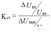
2. The regulator's output resistance
Rout = Rdiff
To find Kst and Rout, an equivalent small-signal circuit of the regulator is considered, Fig. 6. The nonlinear element operates on the stabilization segment, where its AC resistance Rdiff is a parameter of the regulator.
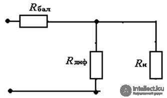
Fig. 6 Equivalent circuit of the parametric voltage regulator
The differential resistance Rdiff is determined from the equation:
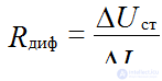
For the equivalent circuit, taking into account that Rload >> Rdiff and Rballast >> Rdiff, we obtain the stabilization coefficient:
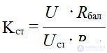
The stabilization coefficient of a parametric voltage regulator is Kst = 5 to 30
To increase the stabilized voltage, Zener diodes are connected in series.
Connecting Zener diodes in parallel is not allowed. To increase the stabilization coefficient, several parametric voltage regulators can be connected in cascade
Transistors
Bipolar, field-effect, IGBT.
Bipolar transistors
A bipolar transistor is a three-layer semiconductor n-p-n or p-n-p structure intended for amplifying the power of electrical signals.
The diagram of the technological structure of a bipolar transistor and its circuit symbols are shown in Fig. 1.
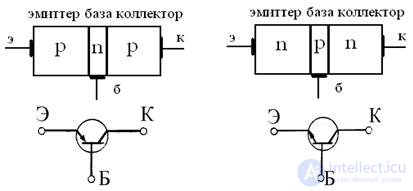
Fig. 1 Diagrams of the technological structures of bipolar transistors
and their circuit symbols.
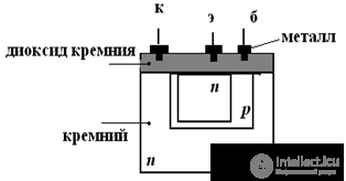
Internal structure of the transistor
Transistor connection configurations
The three layers mentioned have the following names: emitter (E), base (B), collector (C). Three configurations of the bipolar transistor are used to amplify electric power: common-emitter (CE), common-base (CB), and common-collector (CC).
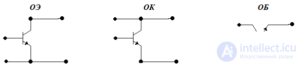
Fig. 2 Transistor connection configurations
Transistor operating modes
1. Active (amplifying) mode
2. Saturation mode
3. Cutoff mode
Static current-voltage characteristics of a BJT
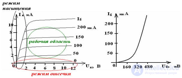
Fig. 3
Amplifying properties of the transistor
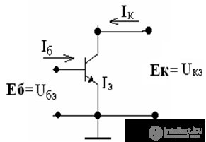
common-emitter transistor configuration
Proof: let
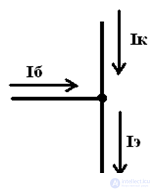
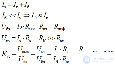
The transistor is controlled by the base current
Equivalent circuit of a bipolar transistor
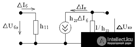
Fig. 4
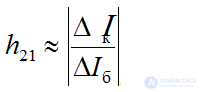
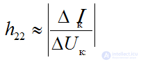
The relationship between the input and output currents and voltages in the transistor, represented as an equivalent two-port network, is expressed by the system of equations of electrical state:
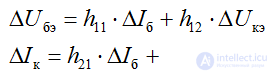
h - transistor parameters
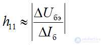
transistor input resistance
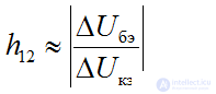
feedback coefficient
DC current gain
output conductance
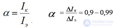
One of the main parameters of a bipolar transistor is the current transfer ratio. When operating in DC mode, for the common-base configuration this is the ratio of the collector current to the emitter current
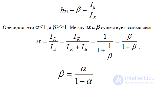
For the common-emitter configuration, the DC current transfer ratio equals the ratio of the collector current to the base current
In addition, as with any two-port network, other main parameters of the transistor are its input and output resistances, which characterize how well the transistor's input and output circuits are matched with other two-port networks.
Graphical determination of the transistor's h-parameters
Uce = Ec - Ic•Rc - the load line
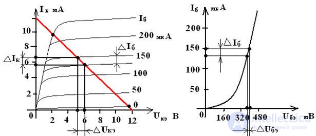
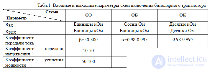
Table 1 gives the comparative parameters of these connection configurations.
Field-Effect Transistors (FETs)
A field-effect transistor is a semiconductor device whose amplifying properties are due to a flow of majority charge carriers passing through a conducting channel controlled by an electric field.
The current is determined by the motion of majority carriers of only one type of charge.
Field-effect transistor - names of the electrodes
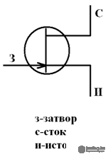
Source - the electrode through which charge carriers flow into the conducting channel;
Drain - the electrode through which charge carriers flow out of the conducting channel;
Channel - the region in the semiconductor where the flow of majority charges is regulated;
Gate - the electrode to which an electrical signal is applied to control the value of the current through the conducting channel.
Types of field-effect transistors
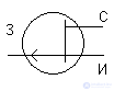
1. Junction field-effect transistor (JFET)
n-channel
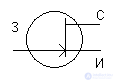
p-channel
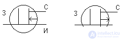
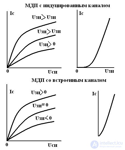
2. MOS (MOSFET) transistors
With a built-in (depletion-mode) channel
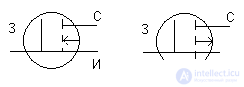
With an induced (enhancement-mode) channel
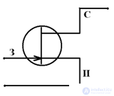
Configurations for connecting field-effect transistors
Common-source configuration
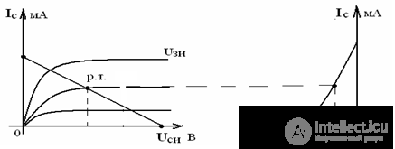
Current-voltage characteristics of a field-effect transistor
with a controlling p-n junction
Main parameters of an FET
• Transconductance of the drain-gate characteristic (DGC)
at Uds = const
S = (∆ Id /∆ Ugs )
• Differential drain (channel) resistance in the saturation region
at Ugs = const
Rd = (∆Uds /∆ Id)
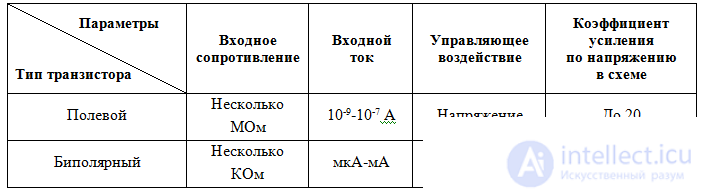
Parameters of field-effect and bipolar transistors
Parameters
IGBT - power transistors
Insulated Gate Bipolar Transistor - a new class of power devices combining the advantages of bipolar and field-effect transistors.
Current control in such devices is achieved by the voltage applied to the gate.
The IGBT was first developed in the research laboratory of General Electric and brought to market by Motorola.
An IGBT is essentially a bipolar p-n-p transistor controlled by a low-voltage MOS field-effect transistor with an induced channel, through a high-voltage n-channel.
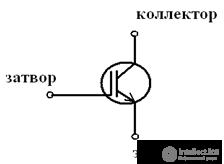
IGBT symbol
Operating principle
The process of turning on an IGBT can be divided into two stages: after a positive voltage is applied between the gate and the source, the field-effect transistor turns on (an n-channel forms between the source and the drain). The movement of charges from the n-region into the p-region causes the bipolar transistor to turn on and a current to flow from emitter to collector. Thus, the field-effect transistor controls the operation of the bipolar transistor.
• The power of the signal applied to the gate of such a device is significantly lower than in bipolar transistors, which allows the use of less powerful control circuits.
• Thanks to their high switching speed, these devices allow the operating frequency of power systems to be increased, and this in turn improves efficiency and size/weight characteristics, i.e. they help solve problems of energy and resource conservation
Thyristors
A thyristor is a semiconductor device based on a single crystal with a four-layer structure containing three p-n junctions, possessing valve-like (rectifying/switching) properties, i.e. a device that allows current to flow in one direction with the ability to control its average and RMS value by controlling the phase at which the thyristor turns on.
Thyristor symbol
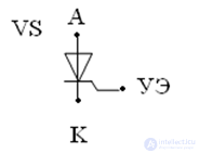
The control electrode allows the moment of turn-on of the thyristor to be controlled even when the potential difference between the anode and cathode is smaller than the breakdown value, provided a forward current is created through the 1st p-n junction. The turn-on moment, or turn-on phase, is called the control angle.
Classification of thyristors:
• Diac (dinistor), without a control electrode; only an anode and a cathode
• Thyristor proper (trinistor), with a control electrode
• Triac, a bidirectional thyristor.
Operating principle
Let us consider the operating principle of a thyristor.
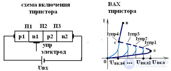
When a voltage Uin is applied to the anode of the thyristor, junctions J1 and J3 are open, while junction J2 is closed, so the entire input voltage is applied across the blocked layer J2. As a result, the thyristor current is very small. As the input voltage increases, the current through the thyristor increases slightly, until junction J2 breaks down; the breakdown voltage is called the turn-on voltage
Uin= Ubr = Uon (point a). The segment |0a| is the reverse branch of junction J2. When junction J2 breaks down, the current through the thyristor increases sharply (point b). Along the segment |bc| all three junctions are under the input voltage, since the voltages of junctions J1 and J3 are equal but opposite in sign. The segment |ac| is the "negative resistance" region of the thyristor.
If a current is applied to the control electrode, the breakdown voltage of the thyristor can be changed. The larger the control current, the lower the turn-on voltage of the thyristor, i.e. the thyristor turns on earlier.
Ictrl4 > Ictrl3 > Ictrl2 > Ictrl1 > 0, hence Uon4
Thyristor parameters:
• Uon - turn-on voltage
• Ictrl - control current
• Uctrl - control voltage
• ton - turn-on time
• toff - turn-off time
• Uon max, at Ictrl=0
An important parameter of a thyristor is the control current Ictrl - the current of the control electrode that causes the thyristor to switch to the conducting state.
Advantages of the thyristor
Thyristors have become widely used thanks to a number of advantages compared to diodes:
• high specific power
• low internal losses, i.e. high efficiency
• wide range of operating temperatures (from -40 to +120 °C)
• instant readiness for operation
• short turn-on time and short recovery time of blocking properties
Industry manufactures thyristors
• for currents I from 2 to 150 A
• for voltages U from 50 to 1000 V
Triac
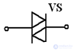
A triac is a bidirectional (symmetrical) thyristor
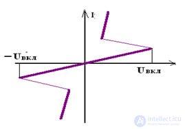
It has a five-layer structure and exhibits thyristor-like characteristics for both polarities of the supply voltage.
Applications
It is widely used because it has two stable states, on and off, and its turn-on and turn-off times are shorter than those of diodes. It is used in power-control devices in household appliances, in adjustable power supplies, in powerful pulse generators, in DC power transmission lines, in static reactive-power comparators, etc.
Current-voltage characteristic of a triac
Controlled rectifiers
Rectifiers that combine the rectification of an alternating voltage with control of the rectified voltage are called controlled rectifiers.
The main element of a controlled rectifier is the thyristor.
Voltage control amounts to controlling, in time, the moment at which the thyristor turns on.
Classification of controlled rectifiers
• single-phase half-wave rectifiers
• single-phase bridge rectifiers: with a full complement of thyristors and with a partial complement, i.e. 2 thyristors and 2 diodes
• three-phase rectifiers with a center-tapped transformer, and bridge rectifiers.
Half-wave controlled rectifier
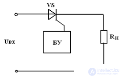
CU - control unit. The control current during the positive half-cycle of e(t) opens the 1st p-n junction and turns on the thyristor. During the negative half-cycle, opening the 1st p-n junction does not cause the 3rd p-n junction to open, because the diffusing carriers do not reach it, since they have almost completely recombined by then.
The average and RMS values of the rectified current (voltage) can be adjusted over a wide range by changing the phase at which the control current is applied.
The presented circuit includes a control circuit, which considerably complicates it, since fairly precise synchronization is required between the frequency of the control current and the frequency of the voltage being rectified.
Timing diagrams
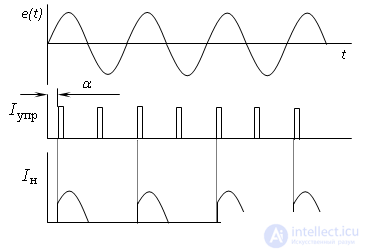
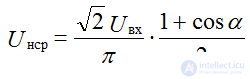
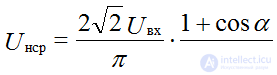
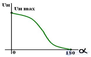
Regulation of the average output voltage of a half-wave rectifier
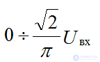
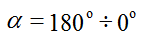
the voltage can be regulated within the range
when the control angle changes
for a full-wave rectifier
control characteristic of a controlled rectifier
Amplifiers of electrical signals
Amplifier operating modes
Depending on the position of the operating point on the transistor's characteristic curves in the quiescent state (with no signal at the input), and on the magnitude of the signal being amplified at the input, three main operating modes of amplifier stages, or amplification classes, are distinguished: A, B, and C. The main characteristics of these modes are nonlinear distortion and efficiency.
Class A is characterized by choosing the quiescent operating point in the middle of the linear region of the input and transfer characteristics (the dependence of collector current on base current). Since in class A the dependence of collector current on base current is practically linear, nonlinear distortion is minimal. However, since the average value of the collector current is much greater than the amplitude of the amplified current, the efficiency of such amplifiers is low, no more than 50%.
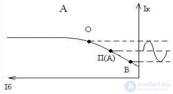
Fig. 1 Class A
The efficiency of an amplifier is defined as the ratio of the output power to the power drawn by the amplifier from the power supply:
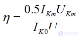
where IKm, UKm are the amplitude values of the amplified collector current and voltage; IK0, UK0 are the collector current and voltage in the quiescent state.
In class B, the operating point lies at the cutoff voltage on the input characteristic (at the start of the transfer characteristic), Fig. 2.
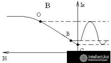
Figure 2. Circuit implementing class B
In class B, current flows through the collector only during the positive half-cycles, when the emitter-base junction opens. If the input signal has a sinusoidal shape, the output signal will have the shape of a half-sinusoid. Clearly, nonlinear distortion in class B is very large, but the efficiency is significantly higher than in class A, since the quiescent current is practically zero. Class B is generally used in push-pull power amplifiers. Efficiency h = 0.8-0.5.
Class C differs from class B in that the operating point in this case is chosen at an input voltage that cuts off the input p-n junction to a value somewhat lower than the amplitude value of the alternating input voltage, Fig. 3.
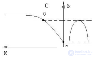
Fig. 3 Circuit implementing class C.
Class C is characterized by the greatest distortion of the amplified signal and the highest efficiency. It is used mainly in self-oscillators (autogenerators)
Voltage amplifier using a BJT
An amplifier is a device intended for amplifying the voltage, current, and power of electrical signals.
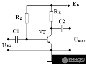
Purpose of the elements
The values of the resistances Rb, Rc, and the supply voltage Ec determine the position of the operating point on the transistor's characteristics in the quiescent state (Ibq, Ubeq, Icq, Uceq).
Ec - to bring the transistor into the amplifying mode.
Rc - to set the gain.
Capacitors C1 and C2 serve to separate the signal - they prevent the DC component of the current from reaching the input of the stage and the load.
Main amplifier parameters
• voltage gain KU;
• input resistance Rin;
• output resistance Rout;
• current gain KI
Analytical method for calculating an amplifier
Let us consider the equivalent circuit
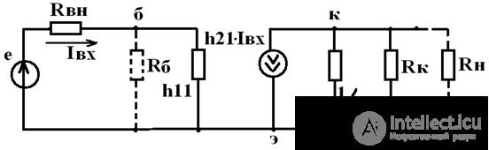
C1 and C2 are absent since Xc is small for alternating current.
Let Rload→∞; then, according to Kirchhoff's first law, for node "c" we write the equations
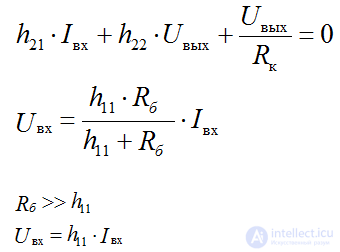
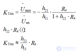
Gain
the "-" sign shows that the input and output voltages are in antiphase)
The gain depends on the transistor's parameters and the value of Rc
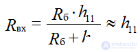
Input resistance
Output resistance
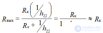
If the load resistance and the input source resistance are taken into account, the gain is equal to:
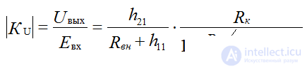
Graphical method for calculating an amplifier
Constructing the transfer characteristic Ic = f(Ib)
1. Quiescent mode Uin=0
We write the equation using Kirchhoff's second law for the collector circuit
Uce =
продолжение следует...
Часть 1 Electronics
Часть 2 - Electronics
Часть 3 - Electronics

Comments