Unlike bipolar transistors, which are controlled by current, insulated-gate transistors are controlled by voltage, since the gate is isolated from the drain and source, giving such transistors a very high input resistance.
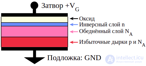
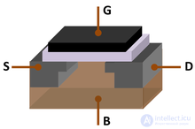
Typical internal structure of a MOS transistor
Classification
By channel type
There are MOS transistors with an intrinsic (or built-in) channel (English: depletion mode transistor) and an induced (or inversion) channel (English: enhancement mode transistor). In devices with a built-in channel, at zero gate-source voltage the transistor channel is open (that is, it conducts current between drain and source); to close the channel, a voltage of a certain polarity must be applied to the gate. The channel of devices with an induced channel is closed (does not conduct current) at zero gate-source voltage; to open the channel, a voltage of a certain polarity relative to the source must be applied to the gate.
In digital and power electronics, typically only transistors with an induced channel are used. In analog electronics, devices of both types are used .
Conductivity type[
The semiconductor material of the channel can be doped with impurities to obtain P-type or N-type conductivity. Applying a certain potential to the gate can change the conduction state of the channel region beneath the gate. If this displaces the majority carriers from the channel while enriching the channel with minority carriers, this mode is called the enhancement mode. In this case, the channel's conductivity increases. When a potential of the opposite sign relative to the source is applied to the gate, the channel is depleted of minority carriers and its conductivity decreases (this is called the depletion mode, which is characteristic only of transistors with a built-in channel) .
For n-channel field-effect transistors, the turn-on voltage is a positive voltage (relative to the source) applied to the gate that exceeds the threshold voltage needed to turn on this transistor. Correspondingly, for p-channel field-effect transistors, the turn-on voltage will be a negative voltage relative to the source applied to the gate that exceeds its threshold voltage.
The vast majority of MOS-technology devices are built so that the transistor's source is electrically connected to the semiconductor substrate of the structure (most often to the die itself). With this connection, a so-called parasitic diode forms between the source and drain. Reducing the harmful effect of this diode involves significant technological difficulties, so engineers have learned to overcome this effect and even use it in certain circuit design solutions. For n-channel field-effect transistors, the parasitic diode's anode is connected to the source, while for p-channel transistors the anode is connected to the drain.
Special transistors
There are transistors with multiple gates. They are used in digital electronics to implement logic elements or as memory cells in EEPROM. In analog circuit design, multi-gate transistors — analogs of multi-grid vacuum tubes — have also found some use, for example in mixer circuits or gain control devices.
Some powerful MOS transistors used in power electronics as electrical switches are equipped with an additional terminal from the transistor channel for monitoring the current flowing through it.
Circuit symbols[
The circuit symbols for semiconductor devices are governed by GOST 2.730-73 .
| |
Induced
channel |
Built-in
channel |
| P-channel |
 |
 |
| N-channel |
 |
 |
| Symbols: G — Gate, S — Source, D — Drain |
Operating features of MOS transistors
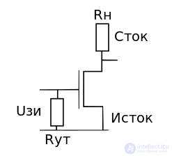
Transistor connection circuit
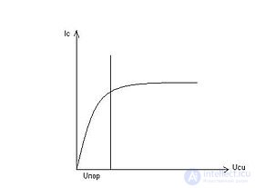
Output (drain) characteristic of an n-type channel field-effect transistor
Field-effect transistors are controlled by the voltage applied to the transistor's gate relative to its source, whereby:


When this voltage changes ( ), the state of the transistor and the drain current change (
 ).
).
- For n-type channel transistors, at
 the transistor is closed;
- At
 the transistor opens and the operating point lies on the nonlinear portion of the field-effect transistor's control (transfer) characteristic:

 — the transistor's specific transconductance;
- With a further increase in the control voltage (), the operating point moves to the linear portion of the transfer characteristic;
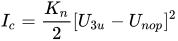 — the Hofstein equation.
Connection features
When connecting powerful MOS transistors (especially those operating at high frequencies), a standard circuit configuration is used:
- An RC snubber network connected in parallel across the source-drain to suppress high-frequency oscillations and large current spikes that occur when the transistor switches due to parasitic inductance and capacitance of the leads. High-frequency oscillations and current spikes increase heat dissipation in the transistor and can cause it to fail if the transistor is operating at its maximum permissible thermal rating. The snubber also reduces the rate of voltage rise across the drain-source terminals, protecting the transistor from self-triggering through the feedthrough capacitance.
- A fast protective diode, connected in parallel across the source-drain in reverse orientation relative to the power supply, shunts the current spikes that arise when a transistor driving an inductive load is turned off.
- If the transistors operate in a bridge or half-bridge circuit at high frequency (for example, in welding inverters, induction heaters, or switch-mode power supplies), then in addition to the protective diode, a Schottky diode is sometimes connected in the drain circuit in the opposite direction to block the parasitic diode. The parasitic diode has a long turn-off time, which can lead to shoot-through currents and transistor failure.
- A resistor connected between the source and gate to bleed off charge from the gate. The gate holds an electric charge like a capacitor, and after the control signal is removed, the MOS transistor may fail to close (or close only partially, leading to increased resistance, heating, and failure). The resistor value is chosen to have minimal effect on the transistor's control while still quickly discharging the gate's electric charge.
- Protective diodes (suppressors) connected in parallel with the transistor and its gate. If the supply voltage across the transistor (or the control signal on the transistor's gate) exceeds the permissible level, for example during pulse interference, the suppressor limits dangerous voltage spikes and protects the gate dielectric from breakdown.
- A resistor connected in series in the gate circuit to reduce the gate recharge current. The gate of a powerful field-effect transistor has high capacitance and is electrically equivalent to a capacitor of several tens of nanofarads, which causes significant current spikes during gate recharging with short control-voltage edges (up to several amperes). Large current spikes can damage the transistor's gate control device.
- A powerful MOS transistor operating in switching mode at high frequencies is controlled using a driver — a special circuit or ready-made chip that amplifies the control signal and provides a large pulse current for rapid recharging of the transistor's gate. This increases the transistor's switching speed. The gate capacitance of a powerful power transistor can reach tens of nanofarads. Rapidly recharging it requires a current of several amperes.
- Optodrivers are also used — drivers combined with optocouplers. Optodrivers provide galvanic isolation of the power circuit from the control circuit, protecting it in the event of a fault, and also provide galvanic isolation relative to ground when driving the upper MOS transistors in bridge and half-bridge circuits. Combining the driver with the optocoupler in a single package simplifies circuit design and assembly and reduces the product's size, cost, and so on.
- In high-current devices with a high level of interference, a pair of Schottky diodes connected in reverse — a so-called diode clamp — is connected to the inputs of chips built on MOS structures (one diode between the input and the common bus, the other between the input and the power bus) to prevent the phenomenon known as "latch-up" of the MOS structure. However, in some cases, using a diode clamp can lead to the undesirable effect of "parasitic power" (when the supply voltage is switched off, the diode clamp can act as a rectifier and continue powering the circuit).


Comments