
Lecture
A phototristor (light-activated thyristor) is a radiation-controlled device with three or more electrical junctions. It is used in power automation systems for switching medium and high power loads, in remote control systems for radio-electronic equipment power supplies, electronic relays, optoelectronic pairs, and more.
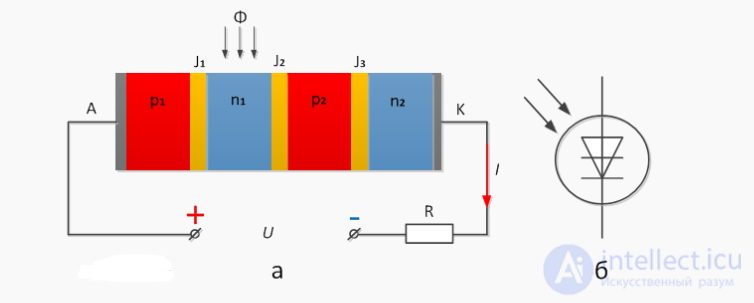
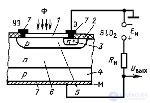 Fig. 8
The design of a phototristor and its connection diagram are shown in Fig. 8. Where: 1 - antireflective coating; 2 - dielectric layer; 3 and 4 - emitter regions of n+ and p- type respectively; 5 and 6 - base regions of p- and n- type; 7 - phototristor leads (CE - control electrode, E - emitter); RL - load resistor.
The optical signal generates nonequilibrium carriers in base regions 5 and 6 of the phototristor, which form a p-n junction reverse-biased by the external source E. The carriers are separated by the electric field of the p-n junction. A photocurrent flows through the junction, and majority carriers accumulate in base regions 5 and 6, lowering the potential barrier of the emitter junctions. This reduction in the potential barrier increases carrier injection from the emitters into the bases. From this point on, the turn-on process of the phototristor proceeds in the same way as when a control current pulse is applied to its base circuit. The phototristor remains in the on state after the light pulse ends. To turn it off, the voltage or current must be reduced below the holding voltage or holding current values. The resistance of the phototristor in the on state is a few ohms or less, and in the off state, hundreds of kilohms. A phototristor is equivalent to a photodiode VD whose photocurrent controls the turn-on of thyristor VT.
The phototristor is equipped with a breakdown protection function, integrated (built) into the device package.
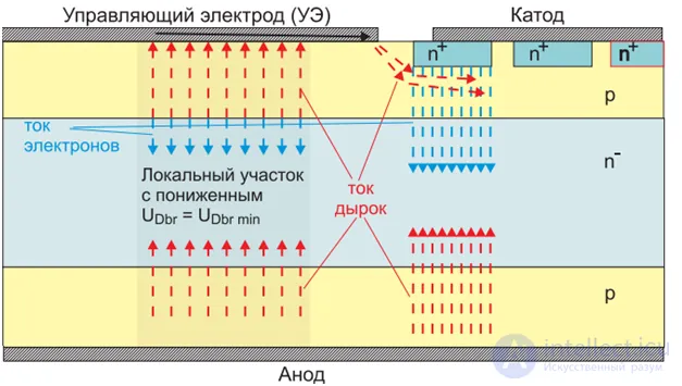
Fig. No. 2. Four-layer structure with a self-protection element against overvoltage breakdown.
The operating principle of the phototristor's protection is that when switching actions occur in connection with unauthorized or critical events.
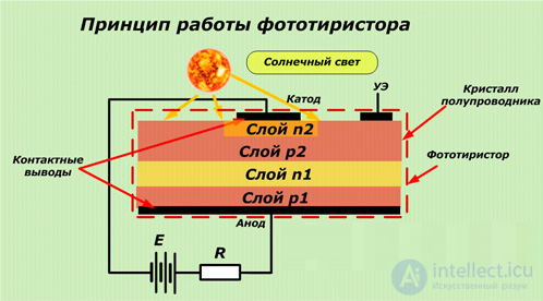
The basis of the designation system for phototristors, as for all semiconductor devices, consists of two types of designations: graphic and symbolic (alphanumeric code). These designations are established by an industry standard and are based on a number of classification criteria.
The graphic symbol is used to create graphic circuit diagrams and is shown in Fig. 8.35.
The graphic symbol of phototristors includes:
The alphanumeric code (symbolic designation) comes in two forms: an alphanumeric designation next to the graphic one
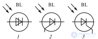
Fig. 8.35. Schematic symbols for phototristors:
designation and the alphanumeric designation code of the phototristor (marking), which classify phototristors according to certain criteria in reference guides.
In circuit diagrams, the symbols next to the graphic designation are: BL1, where BL — photoelement (phototristor), 1 — the sequential number of the device in the circuit.
Industry manufactures several types of phototristors, which have an alphanumeric code in the designation system (marking) that classifies phototristors according to certain criteria in reference guides and consists of the following elements in accordance with industry standard OST 11 336.919—81:
the first element — letters denoting the type of photoelement (TF — phototristor);
the second element — a letter or digit denoting the material from which the sensitive element is made (G or 1 — germanium, K or 2 — silicon);
the third element — a number indicating the sequential development number of the device (from 1 to 9);
the fourth element — a letter defining the subgroup of photoelements (T — phototristor), which is absent in many markings, or a digit indicating the design type from 0 to 5;
the fifth element — a number indicating the maximum permissible current in the on state.
Example of a designation per industry standard OST 11 336.919— 81. TF 130-40: TF — phototristor, 1 — the sensitive element is made of germanium, 3 — sequential development number, 0 — design type, 40 — maximum permissible current of the phototristor in the on state.
- threshold flux Φthr or radiation power Pthr, ensuring guaranteed turn-on of the phototristor at a given source voltage Es;
- minimum duration of the light pulse Tp, ensuring turn-on of the thyristor at a given light flux;
- turn-on time Ton and turn-off time Toff;
- operating wavelength - determined by the material (usually silicon) of the phototristor
- maximum permissible rate of rise of output voltage dUout/dt
- maximum permissible output current Iout.max
maximum operating voltage Umax
threshold power – directly proportional to the maximum operating voltage and the maximum permissible rate of rise of output voltage.
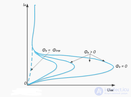
A family of I-V characteristics of the phototristor is shown in Fig. 9, where the light flux is used as a parameter.
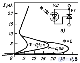 Fig. 9
At a flux of Φ=0, the I-V characteristic does not differ from that of a diode thyristor. The light flux and the base photocurrent of the thyristor are directly proportional.
Therefore, at  the I-V characteristics of the phototristor are similar to those of a triode thyristor.
The value of the threshold light flux can be varied within certain limits by the current of the phototristor's control electrode. This current can be used to electrically control the turn-on and turn-off of the phototristor.
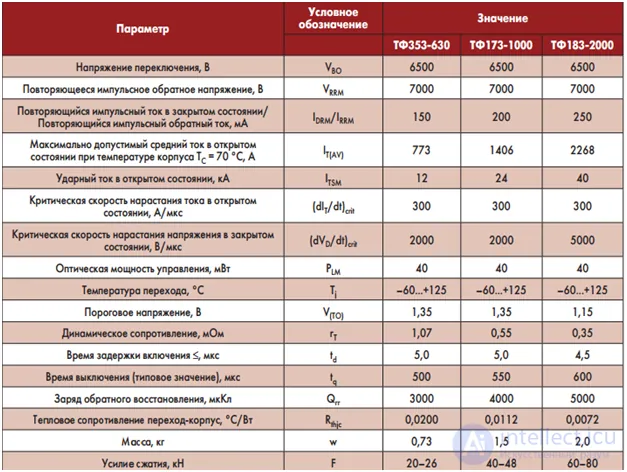
Fig. No. 4. Main parameters and functional characteristics of phototristors.
Phototristors are used in the design of unified thyristor switch modules. One such device is the TF193-2500. It is used as a base component of a converter for the electric power industry. It is successfully used in the design of valves for high-voltage converters.
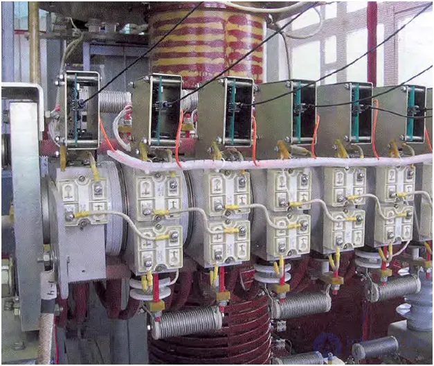
Fig. No. 5. Appearance of a thyristor switch module using TF193-2500 phototristors
Another promising direction in the development of phototristor applications is the design of solid-state switches. The predominant direction for these is the use of pulsed phototristors. They are capable of controlling extremely high power levels within extremely short time intervals. The application range of such switches is quite broad – it includes equipment used to power high-power laser systems. They are used to build circuits that generate extremely powerful electromagnetic fields.
Special switching units for capacitive energy storage devices, designed for pulse currents with an amplitude of 100 kA and a voltage of 12 kV, have been developed based on TFI193–2500 pulsed phototristors.

Comments