
Lecture
Standard graphic symbols are used to denote elements in electronic digital circuits. They help engineers and developers accurately identify components and their functions. Here are a few key symbols:
Logic elements:
Flip-flops:
Digital buses and connections:
Clock signals:
If you are designing or simulating a digital circuit, these symbols will help you organize the project and make it easier to work with online simulators.
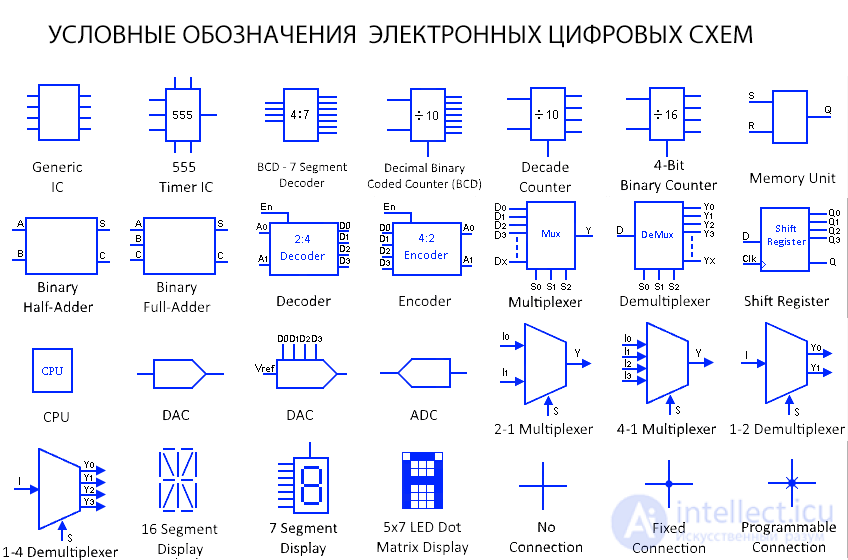
General IC symbol
This is the symbol for a general IC (integrated circuit). It is a small chip made from semiconductor material on which several microelectronic components are fabricated to perform a specific task while reducing size.
555 Timer IC
This is the symbol for the 555 Timer IC. It has three modes of operation: astable (oscillator), monostable (timer), and bistable (flip-flop). It is the most widely used IC in the world, and its applications are virtually limitless depending on the mode in which it is used.
BCD to 7-Segment Decoder
This is the symbol for a BCD to 7-segment display decoder. It converts a binary-coded decimal, which is a 4-bit binary signal, into 7 output lines, each of which drives a separate segment of a 7-segment display.
4-Bit Binary Counter
This is a simple 4-bit binary counter that counts from 0 to 15 and then resets to 0. It operates on a clock signal, incrementing by one digit on each clock cycle. The number 16 represents the MOD number, i.e. the maximum number of states it has. It divides the frequency of the clock signal by this number.
Decade Counter
This is the symbol for a digital decade counter, also known as a frequency divider. It counts from 0 to 9 and then resets, rather than counting in binary digits. Each clock cycle at the input increases the output by 1. This decade counter divides the input frequency (input clock signal) by 10.
Basic Memory Cell
This is the basic memory cell, the building block of a memory unit in any device. It is an SR latch that stores a single bit of data. SR stands for the set and reset function of the latch.
Binary Half Adder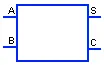
A half adder circuit adds two single-bit binary inputs A and B and produces their sum S and carry bit C. The reason it is called a half adder is that it cannot take into account a carry from previous additions.
Binary Full Adder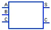
This is the symbol for a digital binary full adder. It adds two single-bit binary numbers A and B and provides their sum S along with a carry C. A full adder also adds the carry from the previous addition, which is why it is called a full adder. Several full adders are chained together to perform addition of multi-bit numbers.
2-to-4 Digital Decoder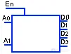
A decoder converts an n-bit binary input into corresponding 2n decimal output lines. The output lines of the decoder are always low, except for one line. This decoder converts a two-bit binary input A0 and A1 into 4 decimal-coded outputs D0, D1, D2, D3. The combination of the input logic A0 and A1 decides which of the output lines will become logic high. The Enable input turns the circuit on and off.
4-to-2 Digital Encoder
A digital encoder converts 2n decimal input lines into n binary output lines. Only one input on the data input lines D should be high at a time. An output in binary code is generated according to the decimal input lines.
Multiplexer or Mux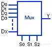
A digital multiplexer, or Mux, is a multi-input, single-output device. It is a digital selector switch that selects one output from several input data lines. Binary combinations of the select bits S0…S2 select a particular data line D0…Dx as the output Y. For example, for S = 010, Y = D2, and for S = 110, Y = D6.
Demultiplexer or DeMux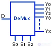
A demultiplexer, or DeMux, is a device with one input and several outputs. It is also a selector switch, and it works the opposite way to a multiplexer. It has a single data input line D and passes it to one of several output lines Y0…Yx, which is selected using the select bits S0…S2.
Shift Register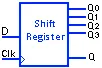
This is a memory unit made up of flip-flops that is used to store temporary data in digital devices. Input data is fed serially into the shift register through the input line D, which is stored in the flip-flop. Data stored in the shift register can be accessed either serially or in parallel using Q and Q0…Q3 respectively.
Processor
CPU stands for Central Processing Unit, also known as the processor; it is a chip inside a computer. It is the brain of the computer, performing tasks by executing instructions carried out by a program.
DAC
This is the general symbol for a DAC, showing only its input and output. A DAC, also known as a digital-to-analog converter, is an electronic IC that converts any digital signal into an analog signal. They are used in systems where the device cannot work with digital data, so the DAC converts the signal into an analog one.
DAC with Digital Input
This is the detailed symbol for a DAC, showing the input ports for the digital signal in binary form and Vref, which is the reference voltage for the generated analog output signal.
ADC
This is the general symbol for an ADC. ADC stands for analog-to-digital converter. It works exactly the opposite way to a DAC. It converts any analog signal into a digital signal in binary format. It is used in almost all digital devices that depend to some extent on analog data.
2-to-1 Multiplexer
This is the symbol for a 2-to-1 multiplexer, or Mux, a digital device with several inputs and one output. The select input S selects either input I0 or I1 as the output Y.
4-to-1 Multiplexer
This is the symbol for a 4-to-1 multiplexer. It selects one of 4 input lines, which passes through to output Y. The select input S is used to select the input line.
1-to-2 Demultiplexer
This is the symbol for a 1-to-2 demultiplexer, used to route a single input line to one of two separate output lines. The select switch S selects one of the two output lines.
1-to-4 Demultiplexer
This symbol is used for a 1-to-4 demultiplexer. It shows a single input line I passed to one of 4 output lines Y, which is selected by the select input S.
Sixteen-Segment Display
This is the symbol for a sixteen-segment display, also known as SISD. It has sixteen LEDs configured in such a geometry as to display characters such as Arabic numerals, Thai numerals, Latin letters, and so on.
Seven-Segment Display
This is the seven-segment display symbol. It is used to display decimal digits and English letters. However, it can be designed to display numerous other characters.
5×7 LED Matrix Display
This is the symbol for a 5×7 matrix display. It has 5 columns and 7 rows of dot-shaped LEDs placed next to each other. It is used to display characters and shapes in digital devices.
No Connection
This is the symbolic depiction of two wires or traces in a digital circuit or diagram that are not connected to each other.
Fixed Connection
This is a visual representation showing a connection between two wires or traces on a circuit diagram.
Programmable Fuse Connection
This is the symbol for a programmable connection. This connection is designed to be closed or opened by blowing a fuse through programming.
Standard symbols are used in digital logic circuits to denote various logic gates. Here are the main ones:
AND:
OR:
NOT:
NAND:
NOR:
XOR (EXCLUSIVE OR):
XNOR (EXCLUSIVE NOR):
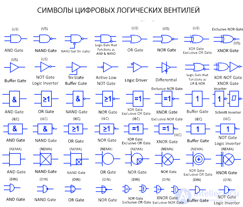
Digital AND Logic Gate
The AND gate performs a logical (inclusive) conjunction (the output is True only if all inputs are True). It provides a "HIGH" logic output only when all of its inputs are "HIGH". And it produces a "LOW" logic when one or all of its inputs are "LOW".
Digital OR Logic Gate
The OR gate performs a logical (inclusive) disjunction (a True output for any True input). The output of the OR gate is logic "HIGH" when one or more of its inputs is logic "HIGH". The output remains logic "LOW" only when all of its inputs are logic "LOW".
Digital NOT Logic Gate
The NOT gate, also known as a logic inverter, is a logic gate with one input and one output. It inverts the input logic. The output signal is logic "LOW" when the input signal is logic "HIGH", and the output signal is logic "HIGH" when the input signal is logic "LOW".
Active-Low NOT Gate
The bubble in front of the gate shows that it is an active-low logic gate. It has the same function as a regular NOT gate.
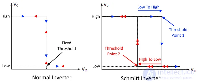
Schmitt Trigger Inverter:
The Schmitt trigger inverter is a logic gate designed using the phenomenon of hysteresis arising from positive feedback within the gate. The main difference between a regular inverter and a Schmitt trigger inverter lies in its threshold level. The former has a fixed threshold that determines LOW and HIGH logic, while the latter has a threshold level that resembles a B-H hysteresis curve, i.e. the low-to-high and high-to-low thresholds differ.
Digital Buffer Gate
A buffer gate has one input and one output. It does not change the input logic. It is mainly used to increase the propagation delay of a signal.
Tri-State Digital Buffer Gate
This type of buffer gate has an additional control pin (also known as the enable pin). It is used to control the flow of logic. If the control pin is HIGH, the input logic flows through; otherwise the output is a "high-impedance Z state".
Digital NAND Logic Gate
The NAND gate is the inverse of the AND gate, or a "NOT AND" gate. Its output is logic "High" when any of the inputs is logic "LOW", and its output is logic "LOW" when all of its inputs are logic "HIGH".
Digital NOR Logic Gate
The NOR gate is the negation, or inverse, of the OR gate, i.e. a "NOT OR gate." It produces "HIGH" logic when all of its inputs are "LOW" logic, and produces "LOW" logic when any of the inputs is "High" logic.
Digital XOR Logic Gate
The XOR gate, also known as the Exclusive OR gate, implements exclusive disjunction (the output is true when exactly one input is true). The output of the XOR gate is HIGH when only one input is HIGH; otherwise the output is LOW.
Digital XNOR Logic Gate
The XNOR gate, also known as the Exclusive NOR gate, is the inverse of the XOR gate. It implements the equality function. The output is True only when the logic of the inputs is the same, i.e. the output is HIGH only when all inputs are "HIGH" or all are "LOW".
Imply Gate
The IMPLY logic gate implements a "logical condition." It forms the statement "If A, then B."
The output of this gate is: "if input A is true, then input B is also true." So when A is true "HIGH" and B is true "HIGH", the output is true "HIGH". When A is true but B is false, the output is false. Now, if input A is false, the output automatically becomes true regardless of input B, i.e. the output is true in both cases.
| A | B | Output |
| 0 | 0 | 1 |
| 0 | 1 | 1 |
| 1 | 0 | 0 |
| 1 | 1 | 1 |
NIMPLY Gate
The NIMPLY logic gate has an inverted output compared to the IMPLY logic gate. It implements the statement "If A, but not B." This means the output is true if and only if input A is true but B is false.
| A | B | Output |
| 0 | 0 | 0 |
| 0 | 1 | 0 |
| 1 | 0 | 1 |
| 1 | 1 | 0 |
In digital circuits, flip-flops are used to store and control the state of bits. Here are the main symbols for various types of flip-flops:
D Flip-Flop (Data or Delay Flip-Flop):
JK Flip-Flop:
T Flip-Flop (Toggle Flip-Flop):
SR Flip-Flop (Set-Reset Flip-Flop):
D Flip-Flop with Asynchronous Reset and Set:
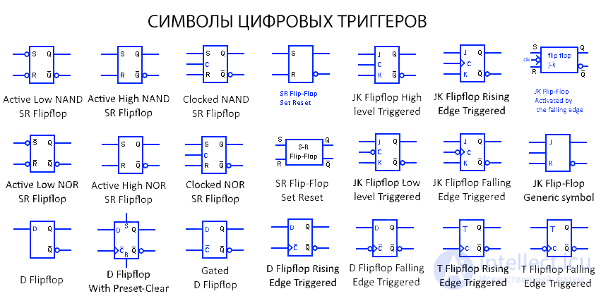
Flip-flops and latches are sequential circuits, and they are the building block for memory units. They store a single bit of data. The output of a sequential circuit depends not only on its current input but also on its previous output.
Active-Low Asynchronous SR NAND Flip-Flop
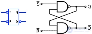
This SR flip-flop, also known as an SR latch, is an asynchronous (clock-independent) sequential circuit made up of only NAND gates. SR stands for the "set and reset" function of the flip-flop. Bubbles at the input show that it is active-low.
When both 'S' and 'R' are LOW, the state is considered invalid, i.e. the output is undefined. This is an invalid state and it is avoided.
| S | R | State | Q next | Q' |
| 1 | 1 | Hold state (no change) | Previous state | Previous state |
| 0 | 1 | Set | 1 | 0 |
| 1 | 0 | Reset | 0 | 1 |
| 0 | 0 | Invalid | X | X |
Active-High SR NAND Flip-Flop
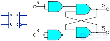
This SR flip-flop works the same as the active-low SR flip-flop, except that its inputs are inverted using NAND gates and inverters. This allows the flip-flop to operate with active-high inputs.
| S | R | State | Q next | Q' |
| 0 | 0 | Hold (no change) | Previous state | Previous state |
| 1 | 0 | Set | 1 | 0 |
| 0 | 1 | Reset | 0 | 1 |
| 1 | 1 | Invalid | X | X |
Clocked SR NAND Flip-Flop
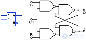
| CLK | S | R | State | Q next | Q' |
| 0 | X | X | Hold (no change) | Previous state | Previous state |
| 1 | 0 | 0 | Hold (no change) | Previous state | Previous state |
| 1 | 1 | 0 | Set | 1 | 0 |
| 1 | 0 | 1 | Reset | 0 | 1 |
| 1 | 1 | 1 | Invalid | X | X |
A clocked SR flip-flop, also known as a gated SR flip-flop, is a modified SR flip-flop with a control input. The clock input controls the state of the flip-flop. When C = 0, the SR flip-flop retains its previous state, i.e. it remains in the hold state. When C = 1, the SR flip-flop operates as a normal active-high flip-flop.
They are used to synchronize with other circuits that use a common clock signal.
Active-Low SR NOR Flip-Flop
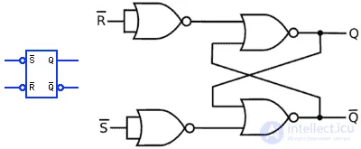
This SR flip-flop is made from four NOR gates. The two NOR gates at the start act as an inverter, which turns this flip-flop into an active-low flip-flop. The bar over the input signals shows that the input is inverted (active-low).
| S | R | State | Q next | Q' |
| 1 | 1 | Hold (no change) | Previous state | Previous state |
| 0 | 1 | Set | 1 | 0 |
| 1 | 0 | Reset | 0 | 1 |
| 0 | 0 | Invalid | X | X |
Active-High SR NOR Flip-Flop
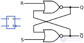
This SR flip-flop is made from just two NOR gates. It works the same way as the SR flip-flop made from NAND gates, but it is active-high.
| S | R | State | Q next | Q' |
| 0 | 0 | Hold (no change) | Previous state | Previous state |
| 1 | 0 | Set | 1 | 0 |
| 0 | 1 | Reset | 0 | 1 |
| 1 | 1 | Invalid | X | X |
Clocked SR NOR Flip-Flop
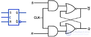
This is a clocked SR flip-flop that uses NOR gates. AND gates are used to control the input signal. When the CLK signal is HIGH, the input signal is passed through and the flip-flop operates normally. When the CLK signal is LOW, the flip-flop remains in a hold state with respect to the S and R signals.
| CLK | S | R | State | Q next | Q' |
| 0 | X | X | Hold (no change) | Previous state | Previous state |
| 1 | 0 | 0 | Hold (no change) | Previous state | Previous state |
| 1 | 1 | 0 | Set | 1 | 0 |
| 1 | 0 | 1 | Reset | 0 | 1 |
| 1 | 1 | 1 | Invalid | X | X |
D Flip-Flops
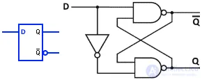
The D flip-flop is also known as the "DATA" or "DELAY" flip-flop. It is a modified version of the SR flip-flop with a single common input D. It stores a single bit of data from the input line D.
When D = 0, the flip-flop is reset and output Q becomes 0. When D = 1, the output is set and Q becomes 1.
| D | State | Q next | Q' |
| 0 | Reset | 0 | 1 |
| 1 | Set | 1 | 0 |
Gated D Flip-Flop (Level-Triggered)
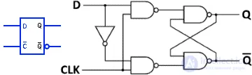
The gated D flip-flop, also known as the level-triggered D flip-flop, has an additional control input known as the "Enable" or "clock" input. When CLK = 0, the D flip-flop retains its previous state. When CLK = 1, it operates as a normal D flip-flop.
| CLK | D | State | Q next | Q' |
| 0 | X | Hold | Previous state | Previous state |
| 1 | 0 | Reset | 0 | 1 |
| 1 | 1 | Set | 1 | 0 |
Rising-Edge Triggered D Flip-Flop
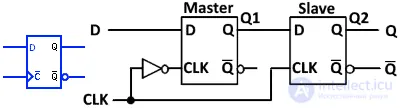
The edge-triggered D flip-flop is also known as a master-slave D flip-flop. It is sensitive to the edge of the clock signal and updates its value only when it detects a clock edge.
It can be designed for either a rising or falling edge. This is a rising-edge triggered D flip-flop. On the rising edge, CLK is applied to the slave flip-flop Q2, and CLK' is applied to the master flip-flop.
This edge-triggered flip-flop updates its state only on the rising edge of the clock signal. Until then, it will retain its state.
| CLK | D | State | Q next | Q' |
| X | X | Hold | Previous state | Previous state |
| Rising edge | 0 | Reset | 0 | 1 |
| Rising edge | 1 | Set | 1 | 0 |
Falling-Edge Triggered D Flip-Flop
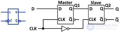
The falling-edge triggered D flip-flop updates its state only on the falling edge of the clock signal. The flip-flop retains its previous state until the falling edge of the clock signal.
In a falling-edge triggered flip-flop, CLK is applied to the master flip-flop, and CLK' is applied to the slave flip-flop.
| CLK | D | State | Q next | Q' |
| X | X | Hold | Previous state | Previous state |
| Falling edge | 0 | Reset | 0 | 1 |
| Falling edge | 1 | Set | 1 | 0 |
D Flip-Flop with Preset and Clear
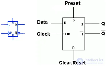
This is an edge-triggered D flip-flop with Preset (SET) and Clear (Reset) functions. It works the same as any edge-triggered D flip-flop. The Preset and Clear inputs set and reset the flip-flop respectively (like an SR flip-flop), independently of the clock edge. Set and Preset can be designed for either active-low or active-high inputs.
| CLK | D | Preset | Clear | State | Q next | Q' |
| X | X | 1 | 0 | Preset | 1 | 0 |
| X | X | 0 | 1 | Clear | 0 | 1 |
| X | X | 0 | 0 | Hold | Previous state | Previous state |
| Rising edge | 0 | 0 | 0 | Reset | 0 | 1 |
| Rising edge | 1 | 0 | 0 | Set | 1 | 0 |
Level-Triggered High JK Flip-Flop
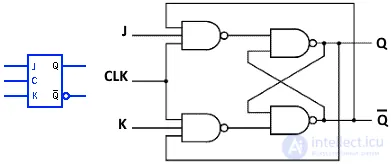
The JK flip-flop is a modified version of the SR flip-flop. The forbidden (invalid) input of the SR flip-flop is used in the JK flip-flop for the toggle function. Apart from the toggle function, the JK flip-flop works the same as the SR flip-flop.
Since this is a level-triggered flip-flop, the CLK signal activates the flip-flop when CLK = 1. The flip-flop retains its state when CLK = 0.
Here is the truth table for a level-triggered JK flip-flop
| CLK | J | K | State | Q next | Q' |
| 0 | X | X | Hold (no change) | Previous state | Previous state |
| 1 | 0 | 0 | Hold (no change) | Previous state | Previous state |
| 1 | 1 | 0 | Set | 1 | 0 |
| 1 | 0 | 1 | Reset | 0 | 1 |
| 1 | 1 | 1 | Toggle state | Q' | Q |
Level-Triggered Low JK Flip-Flop
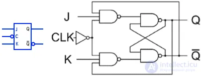
The active-low JK flip-flop is triggered by a low-level CLK pulse. When CLK = 0, the flip-flop is activated, and its state is updated according to inputs J and K. When CLK = 1, the flip-flop retains its previous state regardless of the J and K inputs.
| CLK | J | K | State | Q next | Q' |
| 1 | X | X | Hold (no change) | Previous state | Previous state |
| 0 | 0 | 0 | Hold (no change) | Previous state | Previous state |
| 0 | 1 | 0 | Set | 1 | 0 |
| 0 | 0 | 1 | Reset | 0 | 1 |
| 0 | 1 | 1 | Toggle states | Q' | Q |
JK Flip Flop is triggered on the rising edge
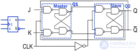
An edge-triggered JK flip-flop is designed by combining two level-triggered JK flip-flops in a Master-Slave configuration. They have the same function as a level-triggered flip-flop, except that they are activated only when a clock edge is present.
A flip-flop triggered on the rising, or positive, edge is activated by the rising edge of the clock signal (from low 0 to high 1). It is designed by connecting CLK to the master flip-flop and CLK' to the slave flip-flop.
| CLK | J | K | State | Q next | Q' |
| X | X | X | Hold (no change) | Previous state | Previous state |
| Rising edge | 0 | 0 | Hold (no change) | Previous state | Previous state |
| Rising edge | 1 | 0 | Set | 1 | 0 |
| Rising edge | 0 | 1 | Reset | 0 | 1 |
| Rising edge | 1 | 1 | Toggle states | Q' | Q |
JK Flip Flop triggered on the falling edge
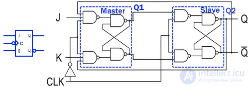
A JK flip-flop triggered on the falling edge is activated by the falling edge of the clock signal.
In a falling-edge-triggered JK flip-flop, CLK is connected to the slave flip-flop Q2, and CLK' is fed to the master flip-flop Q1. Whenever a falling edge is detected, i.e., a transition from high 1 to low 0, the flip-flop updates its state according to the J and K inputs. Otherwise, the flip-flop retains its state no matter what.
| CLK | J | K | State | Q next | Q' |
| X | X | X | Hold (no change) | Previous state | Previous state |
| Falling edge | 0 | 0 | Hold (no change) | Previous state | Previous state |
| Falling edge | 1 | 0 | Set | 1 | 0 |
| Falling edge | 0 | 1 | Reset | 0 | 1 |
| Falling edge | 1 | 1 | Toggle states | Q' | Q |
T flip-flop triggered on the rising edge
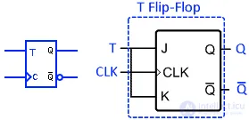
The T flip-flop is a "Toggle" flip-flop and is a modified version of the JK flip-flop. The J and K inputs of the JK flip-flop are joined together, forming a single "T" input.
The T flip-flop changes its state when T = 1, i.e., Q = Q'. When T = 0, the flip-flop retains its previous state.
Since this is a rising-edge T flip-flop, the flip-flop will toggle only when a positive edge of the clock signal is present, i.e., the clock signal changes from 0 to 1. Otherwise, the flip-flop will remain in the hold state.
| CLK | T | State | Q next | Q' |
| X | X | Hold (no change) | Previous state | Previous state |
| Rising edge | 0 | Hold (no change) | Previous state | Previous state |
| Rising edge | 1 | Toggle states | Q' | Q |
T Flip Flop triggered on the falling edge
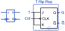
A falling-edge-triggered T flip-flop is created by connecting the inputs (J and K) of a falling-edge-triggered JK flip-flop. It is activated when a falling edge is detected in the clock signal; otherwise, the flip-flop will retain its previous state regardless of the input logic.
| CLK | T | State | Q next | Q' |
| X | X | Hold (no change) | Previous state | Previous state |
| Falling edge | 0 | Hold (no change) | Previous state | Previous state |
| Falling edge | 1 | Toggle states | Q' | Q |

Comments