
Lecture
Optoelectronics uses optical and electronic phenomena in materials, and the interactions between them, to transmit, process, and store information. The element base of optoelectronics consists of optoelectronic devices — optocouplers.
An optoelectronic pair, or optocoupler, is a semiconductor device consisting of a light-emitting element and a photodetector element, connected to each other through an optical channel. The light emitter, photodetector, and optical channel (which provides galvanic isolation between input and output) are structurally combined in a single package.
An optocoupler (or optoisolator) is an electronic device consisting of a light emitter (usually an LED, or in early devices a miniature incandescent lamp) and a photodetector (bipolar or field-effect phototransistors, photodiodes, phototriacs/phototransistors, photoresistors), connected by an optical channel and, as a rule, combined in a common package. The operating principle of an optocoupler consists of converting an electrical signal into light, transmitting it through the optical channel, and then converting it back into an electrical signal.
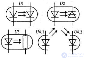
Fig. Schematic symbol of optocouplers
By degree of integration
By type of optical channel
By type of photodetector
By type of light source
Optocouplers with a field-effect transistor or phototriac are sometimes called optorelays or solid-state relays.
Two directions can currently be distinguished within optoelectronics.
There are two classes of optical elements that can be used in building optical computers:
They represent, respectively, the electro-optical and optical directions.
The type of photodetector determines the linearity of the optocoupler's transfer function. Resistive optocouplers are the most linear and hence most suitable for use in analog devices, followed by optocouplers with a receiving photodiode or a single bipolar transistor. Optocouplers with compound bipolar transistors or field-effect transistors are used in pulse (switching, digital) devices, where transmission linearity is not required. Optocouplers with phototriacs are used to provide galvanic isolation of control circuits from drive circuits.
An optocoupler is a single unit consisting of a radiation source and a receiver, connected to each other via an optical channel. The block diagram of an optocoupler is shown in Fig. 8.8.
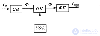
Fig. 8.8. Block diagram of an optocoupler
The input signal, for example an electric current Iin, is converted by the light emitter LE into a light flux Φ, whose energy is proportional to the input signal. The light flux travels through the optical channel OC to the photodetector PD, where it is converted into an output electric current Iout proportional to the light flux. Using an optical-channel control device OCC, the light flux can be controlled by changing the physical properties of the optical channel itself.
Thus, a double energy conversion takes place in optocouplers: electrical into light, and light back into electrical. This gives optocouplers a number of entirely new properties and makes it possible to build electronic devices with exceptionally distinctive parameters and characteristics based on them. For example, using optocouplers makes it possible to achieve nearly ideal electrical isolation between elements of a device (resistance up to 1016 Ω, coupling capacitance down to 10-4 pF). In addition, such properties of optocouplers as unidirectional information flow, absence of feedback from output to input, high noise immunity, a wide bandwidth (from zero to hundreds or even thousands of megahertz), and compatibility with other (semiconductor) devices can be used effectively. This makes it possible to use optocouplers for signal modulation, measurements in high-voltage circuits, and matching low-frequency circuits with high-frequency ones and low-impedance circuits with high-impedance ones.
The drawbacks of optocouplers include the temperature dependence of their parameters, and low efficiency and transfer ratio.
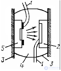
Fig. 8.9. Structure of an optocoupler: 1 – leads; 2 – photodetector; 3 – package; 4 – optical medium; 5 – LED
The structure of an optocoupler is shown in Fig. 8.9. LEDs based on gallium arsenide phosphide (GaAsP) or gallium aluminum arsenide (GaAlAs) are usually used as emitters in optocouplers, as they are characterized by high brightness, high speed, and a long service life. In addition, they are well matched in spectral characteristics with silicon-based photodetectors. Photoresistors, photodiodes, phototransistors, and phototriacs can be used as photodetectors.
Photodiodes and phototransistors have become the most widely used radiation receivers in optocouplers, since their characteristics and parameters allow them to work together with integrated circuits. Phototriacs are widely used in optocouplers as switching power amplifiers controlled by light radiation. Light transmission in optocouplers is carried out through an optical channel, whose role can be played by various media. The purpose of the optical channel is to transmit the maximum amount of light energy from the emitter to the receiver. The transmitting medium can be air, various immersion media, or optical fibers 1 m or more in length. Fiber-optic communication lines make it possible to raise the breakdown voltage of the isolation between the input and output of an optocoupler to 150 kV, which makes it possible to use optocouplers for measurements in high-voltage circuits.
The input parameters of optocouplers are: the rated forward input current of the LED Iin.rated and the forward voltage drop across it Uin at the rated value of input current; the input capacitance Cin under a given operating mode; the maximum permissible input current Iin.max; and the maximum permissible reverse input voltage Uin.rev.max.
The output parameters of optocouplers are: the maximum permissible reverse voltage Uin.rev.max applied to the output; the maximum permissible output current Iout.max; the output capacitance Cout; and the illuminated Rlight and dark Rdark output resistances (for photoresistive optocouplers).
Among the transfer parameters, the primary ones are the current transfer ratio KI = (Iout / Iin)·100 or the differential current transfer ratio KI,d = (dIout / dIin)·100, expressed as percentages.
The speed of an optocoupler is evaluated by applying a rectangular pulse to its input and measuring the delay time td from the moment the pulse is applied to the moment the output current reaches 0.1 of Iout.rev.max, and also by the rise time tr of the output current from 0.1 to 0.9 of its maximum value. The sum of the delay time and the rise time is called the turn-on time ton. The speed of the photodetector is characterized by its frequency properties, i.e., the frequency of a sinusoidally modulated light flux at which the sensitivity of the photodetector, owing to its inertia, decreases by a factor of  .
.
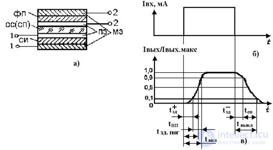 Fig. 1
An optocoupler is used as an electrical isolation element in digital and pulse devices, analog-signal transmission devices, and automation systems for contactless control of high-voltage power supplies, among others. It is a component element of optical integrated circuits. In the design of the optocoupler (Fig. 1a), LE is the light emitter, PD is the photodetector, OM (OS) is the optical medium, ME are metal electrodes, and TE are transparent electrodes. LEDs, lasers, and other emitters are used as light emitters in optocouplers, while photodiodes, phototransistors, photoresistors, and phototriacs are used as photodetectors. Depending on the type of photodetector used, optocouplers are classified as diode, transistor, thyristor, and resistive types.
The operating principle of an optocoupler is shown in Fig. 1. An electrical signal, for example a current pulse IIN (Fig. 1b), is fed to the input of the optocoupler and is converted by the light emitter into a light-flux pulse. The light pulse is emitted at the operating wavelength toward the photodetector, passes through the optical medium with low attenuation, and is converted into an electrical signal in the photodetector. The shape of the output current pulse is shown in (Fig. 1c). Conversion of the electrical signal into an optical signal is carried out by modulating the optical carrier in the light emitter. Galvanic isolation of the input circuit 11 and output circuit 22 of the optocoupler is achieved through an optically transparent dielectric medium between the receiver and the emitter, and all components of the optocoupler must be optically matched. This is achieved by an appropriate choice of materials. Fig. 2 shows examples of matched pairs of semiconductor materials for the photodetector and light emitter over the wavelength range of 0.2–20 μm. LEDs are predominantly used as light emitters in optocouplers.
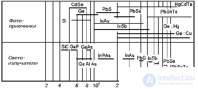
Fig. 2
The use of lasers in optocouplers is economically justified only in high-speed systems. Given that the emission spectrum of the LEDs used in optocouplers is relatively narrow, the sensitivity of the photodetector should be at its maximum at the operating wavelength of the light emitter.

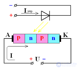
schematic symbol of a phototriac
 =
=
A phototriac is similar to an ordinary thyristor, except that it is controlled not by a gate electrode but by rays (apparently infrared) emitted by an LED. The main advantage of a phototriac over an ordinary thyristor is the galvanic isolation of the power circuit from the control circuit.
Optically triggered SCRs are a special type of symmetric semiconductor power device that can be used most effectively in phase-controlled converter devices. A phototriac is a semiconductor assembly consisting of two elements combined into a single unit: a power silicon (Si) phototriac and a low-power gallium arsenide (GaAs) control LED. Optical isolation of the power and information sections not only simplifies control of such a thyristor but also significantly increases the noise immunity of high-power converters and automatic control systems built on their basis, particularly high-voltage systems. Control drivers for devices isolated via an optical channel generally have a simpler design and lower power than drivers for ordinary thyristors with an external control electrode.
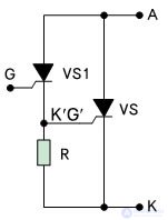
Fig. 1. Equivalent electrical circuit of a thyristor with a regenerative gate electrode
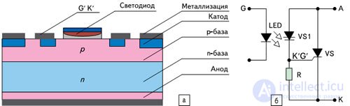
Fig. 2. Power phototriac with a regenerative gate electrode: a) simplified structure; b) equivalent electrical circuit
The light-flux power required to switch a phototriac depends on the depth of the junctions beneath the crystal surface and the rate of surface and bulk recombination of charge carriers, and it increases with wavelength. The efficiency of photogeneration of carriers is determined not only by the emission spectrum of the LED used but also by the design features of the device: the radiation pattern; the angles and point of incidence of the radiation beam; the ratio of the optical window area to the total crystal area; the design of the light channel; and the properties of the materials used.
The structure of a phototriac is practically no different from that of an ordinary thyristor with a gate electrode, except for possible changes in junction depths and the doping levels of individual layers, for example to reduce the required gate charge. Discrete low-frequency devices and phototriac modules are currently available for currents up to 1 kA and voltages up to 2.4 kV, which makes it possible to build controllable devices with an output power of several megawatts (for standard industrial mains voltages of 50, 60, and 400 Hz). Work is also underway on high-speed optically triggered thyristors for operating frequencies above 500 Hz. The level achieved in commercial industrial designs is reflected in Table 1 (here and below the standard system of parameter notation for thyristors [4, 5] is used) [6-9].
A phototriac can be conditionally divided into two parts: an LED and a phototriac. Let us consider the operation of the phototriac. A phototriac has a four-layer pnpn structure (three pn junctions). When voltage U is applied to it, the middle pn junction remains closed. It can be opened in two ways:
- by raising the voltage between the anode A and the cathode K, in which case the control voltage on the LED need not be applied, i.e., Uctrl. = 0;
– by applying a control voltage to the LED. When the pn junction of the thyristor is illuminated, a photo-EMF arises in it. Keep in mind that voltage U already exists between the anode and the cathode.
The greater the control current (light intensity), the lower the voltage required between the anode and cathode to open the phototriac. Note! In the open state, when the voltage drop between A and K is small and the current is high, the thyristor is no longer controllable. To switch it off, the supply voltage U must be removed. It is a mistake to think that an ordinary thyristor is controlled only by the control current. In fact, it is merely turned on by that current. Study Fig. 2 carefully.
To avoid confusion, industry also produces gate turn-off thyristors, or GTOs. Unlike ordinary thyristors, these can be controlled without removing the voltage U. To turn on a GTO thyristor, a positive voltage is applied to the gate electrode; to turn it off, a negative voltage is applied. However, such thyristors are designed for large currents and have larger dimensions, and are produced in disc (puck) and stud (bolt-down) packages.
The main parameters of optocouplers can be divided into four groups.
The input parameters characterize the operating mode of the light emitter. If an LED is used as the light emitter, its electrical parameters form the basis of the optocoupler's input parameters:
Output parameters.
The output parameters are characterized by the operating modes and characteristics of photodetectors such as photoresistors, phototransistors, etc.
- Maximum permissible output current IOUT.MAX through the photodetector when the optocoupler is on
- Maximum permissible reverse output voltage UOUT.REV.MAX.
- Output capacitance COUT.
Signal-transfer parameters.
The transfer parameters generally characterize the frequency and pulse properties of optocouplers.
- Transfer ratio of the optocoupler Ki. This ratio has a different physical meaning for different types of optocouplers:
A distinction is made between the static current transfer ratio Ki=(IOUT-IQ)/IIN and the differential current transfer ratio Ki,d=dIOUT/dIIN for diode and transistor optocouplers. If the output transistor of the photodetector operates in saturation mode, the static transfer ratio is determined for the current IOUT corresponding to the saturation voltage USAT. The transfer ratio of resistive optocouplers is the ratio of the dark and illuminated output resistances, i.e., Ki=RDARK/RLIGHT. For a phototriac, the transfer ratio has no physical meaning, since once switched on, the phototriac remains in that state regardless of the input voltage. Therefore, the parameter for this element is the turn-on current — the minimum input current of the optocoupler IIN that switches the phototriac to the on state — as well as the maximum permissible noise input current INOISE.IN, at which the phototriac does not yet turn on. The parameter INOISE.IN characterizes the noise immunity of the thyristor-type optocoupler against false triggering.
- Maximum signal transfer rate FMAX — the number of signals that can be transmitted through the optocoupler per unit time without losing or falsely generating even a single one of them. It characterizes the speed of an optocoupler operating in digital-signal transmission devices.
- Rise time tR and fall time tF — the rise time is measured from the level of 0.1 IOUT.MAX to the level of 0.9 IOUT.MAX (Fig. 1c).
- Pulse-edge delay time tD — the turn-on delay time, measured from the moment the input signal arrives to the moment the output rises to the level of 0.1 IOUT.MAX.
- Logic delay time tD.LOGIC — the delay time from the moment the signal is applied to the optocoupler's input to the moment the output signal rises to the level of 0.5 IOUT.MAX.
- The speed of optocouplers in pulse and digital circuits is evaluated by the total switching time
tsw=ton+toff, where ton=t+D+tR, and toff=t-D+tF.
- Current transfer ratio:
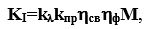 , (1)
, (1)
Where:  - the spectral matching coefficient, kPR – the transparency coefficient of the optical medium,
  – the external quantum yield of the light emitter, M – the gain factor of the photodetector.
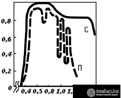
Fig. 3
The spectral matching coefficient of the light emitter  , of the photodetector, and of the optical medium depends on the difference in spectral characteristics between the light emitter and the photodetector within the working wavelength range, and on the spectral transmission characteristic of the optical medium. Fig. 3 shows the spectral transmission characteristics of glass and polymer, which are used as optical media in optocouplers. The vertical axis shows the normalized spectral transmission characteristic of the optical medium. In the near-infrared wavelength region, the polymer exhibits resonant absorption of radiation by the chemical groups OH, CH3, CH2, NH2, NH, and others. Narrow dips in the transmission spectral characteristic correspond to resonant absorption. Over the working wavelength range, the transmission coefficient of the optical medium should be close to unity.
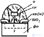 Fig. 4
Transparency coefficient of the optical medium kpr To increase this coefficient, the materials of the light emitter, photodetector, and optical medium are selected according to their refractive index; foreign inclusions at the light emitter–optical medium–photodetector interfaces are technologically eliminated; homogeneous media, anti-reflective coatings, and light guides are used in the light emitter–photodetector coupling channel; and the design of the optocoupler is improved.
External quantum yield of the light emitter  To increase the external quantum yield of an LED, one must, first, reduce the loss of generated photons within the generation region, achieve total internal reflection at the semiconductor–optical medium interface, and reduce losses due to edge and back emission (edge and back emission losses of the LED are reduced in the optocoupler design shown in Fig. 4); second, increase the injection coefficient of the LED's electrical junction; and third, reduce the fraction of nonradiative and competing recombination in the LED's junction, i.e., increase the internal quantum yield.
Also, to increase the quantum yield it is necessary to select optimal LED materials, use heterojunctions in their structure, reduce the reflection coefficient at the optical-medium–semiconductor interface, and reduce losses from passive absorption in the semiconductor that do not produce nonequilibrium carriers, as well as recombination losses.
Gain factor M of the photodetector (phototransistor). As the gain factor M of the photodetector increases, the speed of the optocoupler decreases in most cases. Using rational photodetector structures, such as a photodiode-transistor combination, makes it possible to obtain an acceptable gain factor without a significant reduction in the optocoupler's speed.
Galvanic isolation parameters:
- Maximum permissible peak voltage between the input and output of the optocoupler UISO.PK.MAX.
- Maximum permissible voltage between the input and output Uiso.max.
- Coupling capacitance CISO. This is the capacitance between the input and output of the optocoupler, which characterizes its frequency properties. This parameter should be minimized, for which the optocoupler design shown in (Fig. 6) is used.
- Galvanic isolation resistance RISO. — this is the resistance between the input and output of the optocoupler.
- Maximum permissible peak voltage characterizes the dielectric strength of the optocoupler and is usually UISO.PK.MAX>1 kV.
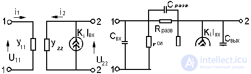 Fig. 5
In analog-signal transmission mode, an optocoupler can be represented as a linear two-port network with Y parameters. Since the signal in an optocoupler is transmitted only from the light emitter to the photodetector, the two-port network must be unidirectional. Its circuit contains only ideal generators, and the conductance of the two-port network's feedback path y12=0. Fig. 5 shows the equivalent circuit of an optocoupler with ideal galvanic isolation. The input electrical signal of a real optocoupler passes to the output of the two-port network through the isolation parameters RISO and CISO. Taking the isolation parameters into account, the equivalent circuit is transformed as follows: capacitor CIN and resistor rle.diff model the input capacitance and differential resistance of the light emitter; capacitor COUT and resistor rpd.diff model the output capacitance and output differential resistance of the photodetector; capacitor CISO and resistor RISO account for the isolation capacitance and resistance of the optocoupler; and the current source KiIin represents the conversion of the input signal by the optocoupler.
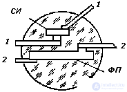 Fig. 6
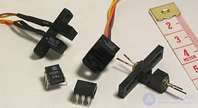
Various types of optocouplers
Optocoupler designs vary: assembled from discrete elements, film-type, and monolithic. Let us consider examples of optocoupler designs built from discrete elements. In the packageless optocoupler (Fig. 6), LE is the light emitter; PD is the photodetector; OM is the optical medium; 1 – leads of the light emitter; 2 – leads of the photodetector. The light-emitter and photodetector crystals are placed in the optical immersion medium strictly in parallel. Organic polymer optical adhesives are mainly used as the optical medium. LEDs commonly used in optocouplers have a ring-shaped emitting region with an ohmic contact located in the center, outside the active emission area. In this design, with a minimal light-emitting area of the LED, energy losses due to shading and edge effects are reduced, and the requirements on the precision of the LED-to-photodetector alignment are relaxed.
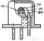 Fig. 7
To increase the transfer ratio of the optocoupler, the sensitive area of the photodetector greatly exceeds the emitting area of the LED. The photodetector structures of optocouplers are made mainly of silicon. The most widely used are p-i-n structure photodiodes, bipolar phototransistors, phototriacs, photodiode-transistor structures, and others.
The design of an optocoupler in a metal-glass package is shown in Fig. 7. To reduce the isolation capacitance to 10-3–10-4 pF, a grounded metal mesh GM is built into the optical medium, or glass with a conductive coating made of materials such as SnO2 or In2O3. The isolation resistance of the optocoupler reaches values of 1014–1016 Ω.
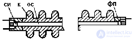
Fig. 8
Edge and back emission losses of the LED are reduced in the optocoupler design shown in Fig. 4, where R is the reflector; RC(M) is the metal ring lead of the p-region of the photodetector, insulated from the n-region by a dielectric SiO2 layer. The reflector directs the LED's rays, shown in the figure by arrows, onto the sensitive area of the photodiode and increases the optocoupler's transfer ratio by about a factor of two. A design version of an optocoupler with galvanic isolation of up to several tens of kilovolts is shown in Fig. 8. Isolation is provided by a rigid glass light guide OM, placed inside the optocoupler's package P.
An example of a film-type optocoupler design is shown in Fig. 1a. A layer of SnO2 is deposited on both sides of a glass substrate GS, forming transparent electrodes TE. On one of the transparent electrodes, a thin film layer of phosphor — zinc sulfide (ZnS) activated with copper (Cu) and manganese (Mn) impurities — is formed by vacuum evaporation, followed by a metal electrode ME. On the other transparent electrode, a photoresistive layer of cadmium sulfide with sensitivity centers of copper atoms (CdS:Cu) is deposited, onto which a metal electrode ME of comb structure is then sputtered. The thin-film phosphor light emitter LE of the optocoupler can operate at low DC voltage. The luminescence is caused by excitation of manganese atoms in the phosphor by "hot" (high-energy) electrons generated in the p-Cu2S–n-ZnS(Mn) heterojunction in the surface layer of the film. The light flux propagates toward the optocoupler's photoresistor photodetector PD through the glass substrate and the transparent electrodes, which form the optical medium.
The advantages of optoelectronic pairs include nearly ideal galvanic isolation, immunity of the optical communication channel to electromagnetic interference, compatibility of input and output signal parameters with integrated circuits, and broad functional capabilities.
The disadvantages of optoelectronic pairs are low signal-energy conversion efficiency, high power consumption, temperature dependence of parameters, a relatively narrow operating temperature range, a limited service life, design imperfections, and others — although most of these are temporary in nature.
Let us give a brief description of some of the most common types of industrial optocouplers.
Photodiode optocoupler.
Its schematic symbol is shown in Fig. 8.10a. A gallium arsenide-based LED is used as the emitter.
Silicon photodiodes, which are well matched in spectral characteristics and speed with gallium arsenide LEDs, are used as photodetectors in diode optocouplers.
The current transfer ratio of a diode optocoupler is small (KI = 1.0 1.5%), but diode optocouplers are the fastest.
As a circuit element, the photodetector of a diode optocoupler can operate in two modes: as a photoconverter with an external power supply, or as a photogenerator without an external power supply.
Taking into account the dependence of the LED's light flux on the input current Iin through the LED, one can find the dependence of the load resistor current IL or the voltage UL across it on the optocoupler's input current, i.e., IL = f(Iin) or UL = φ(Iin).
It should be taken into account that, to transmit the maximum energy, the load resistor must be matched to the optocoupler's output resistance.
Phototransistor optocoupler (Fig. 8.10b). Compared to a photodiode optocoupler, a silicon phototransistor is used as the photodetector. Being a base-current amplifier, the phototransistor has a substantially higher sensitivity than a photodiode, so the current transfer ratio of a phototransistor optocoupler is KI = 50100%, and for an optocoupler with a compound phototransistor it can reach 800% or more.
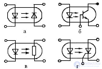
Fig. 8.10. Schematic symbols of optocouplers: photodiode (a), phototransistor (b), photoresistor (c), phototriac (d)
A drawback of phototransistors is that, compared with photodiodes, they are much more sluggish, with a speed of 10-4–10-5 s.
Photoresistor optocoupler (Fig. 8.10c). Photoresistors based on cadmium selenide or cadmium sulfide (CdSe, CdS) are sometimes used as photodetectors in optocouplers, together with spectrally matched LEDs based on gallium phosphide or gallium arsenide phosphide (GaP, GaAsP) as the emitter. The speed of photoresistive optocouplers is entirely determined by the speed of the photodetector, which is about 100–200 μs.
Phototriac optocoupler (Fig. 8.10d) incorporates a phototriac as the photodetector. The speed of a phototriac optocoupler is determined by the turn-off time of the phototriac, during which the device switches from the on state to the off state, and it amounts to tens of microseconds.
Depending on the type of photodetector, optocouplers can be used in electronic devices for switching, conversion, matching, modulation, and so on. They can also be used as small-sized pulse transformers, relays for switching voltages and currents, in self-oscillators, feedback circuits, and so forth.
Optocouplers with an open optical channel serve as various sensors (for displacement, "object edge," etc.). Optoelectronic integrated circuits, in which optocouplers and an integrated circuit are combined in a single package, are often used in data transmission devices. The photodetector of such a microcircuit can be fabricated on the same silicon crystal as the transistor circuit, as a single unit.
Optoelectronic devices with a controllable light guide can be used as logic cells in frequency converters, in indicator-switching devices, liquid-type indicators, devices for measuring small displacements, tactile sensing devices for robots, and so on. These devices have high speed, noise immunity, and can be used in aggressive and explosive environments.
Recently, in manufacturing optoelectronic devices, it has become possible to move the radiation source and receiver away from the measurement zone (from the object being monitored) by tens of meters using fiber-optic elements — optical fiber waveguides (bundles of glass fiber strands).
Optoelectronic devices are widely used in computing technology, automation, and monitoring and measurement instruments. In the future, the use of these devices will continue to expand as their characteristics — reliability, durability, and temperature stability — improve.
Optocouplers have several areas of application that make use of their various properties:
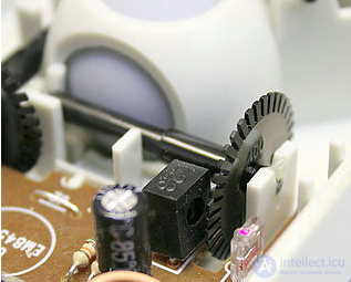
Optical coordinate counter in a mechanical mouse
Optocouplers with an open optical channel accessible for mechanical actuation (interruption) are used as sensors in all kinds of presence detectors (for example, a paper detector in a printer), end-of-travel or start sensors (similar to a mechanical limit switch), and counters and discrete speedometers built on them (for example, coordinate counters in a mechanical mouse, anemometers).
Optocouplers are used for galvanic isolation of circuits — transmitting a signal without transmitting voltage — for contactless control and protection. Some standard electrical interfaces, such as MIDI, mandate the use of optocoupler isolation. There are two main types of optocouplers intended for use in galvanic isolation circuits: optocouplers and optorelays. The main difference between them is that optocouplers are generally used for transmitting information, while optorelays are used for switching signal or power circuits.
Optocouplers
Transistor or integrated optocouplers are generally used for galvanic isolation of signal circuits or circuits with low switching current. Bipolar transistors, control circuits for digital inputs, and specialized circuits (for example, for driving a power MOSFET or IGBT — opto-drivers) are used as the switching element.
Properties and characteristics of optocouplers
Dielectric strength (the permissible voltage between the input and output circuits) depends on the device's construction. Optocouplers for galvanic isolation are manufactured in DIP, SOP, SSOP, and Mini flat-lead packages. Each package type has its own characteristic isolation voltage. To ensure high breakdown voltages, the optocoupler's construction must provide as large a distance as possible not only between the LED and the photodetector, but also along both the internal and external surfaces of the package. Manufacturers sometimes produce specialized optocoupler families that comply with international safety standards. These optocouplers are characterized by increased dielectric strength.
One of the main parameters characterizing a transistor optocoupler is the current transfer ratio. Optocoupler manufacturers perform sorting, assigning a particular ranking based on the transfer ratio, which is indicated in the part designation.
The lower operating frequency of an optocoupler is unlimited: optocouplers can operate in DC circuits. The upper operating frequency of optocouplers optimized for high-frequency transmission of digital signals reaches hundreds of MHz. The upper operating frequencies of linear optocouplers are substantially lower (units to hundreds of kHz). The slowest optocouplers, which use incandescent lamps, are in effect efficient low-pass filters with a cutoff frequency on the order of a few Hz.
Noise in transistor optocouplers
Transistor optocouplers are characterized by the appearance of noise caused, on one hand, by the presence of feed-through capacitance between the LED and the transistor's base, and on the other hand, by the presence of parasitic capacitance between the collector and base of the phototransistor. To combat the first type of noise, a special shield is added to the optocoupler's construction. The second type of noise can be avoided by correctly selecting the optocoupler's operating conditions.
Types of optocouplers for galvanic isolation
Application examples for optocouplers
Photorelays
Photorelays (solid-state relays) are typically used for switching circuits with high switching currents. A pair of back-to-back connected MOSFET transistors is usually used as the switching element, which allows the photorelay to operate in AC circuits.
Properties and characteristics of photorelays
Photorelays come in three topologies. Normally open — topology A, normally closed — topology B, and changeover — topology C. The normally open topology closes the switching circuit only when control voltage is applied to the LED. The normally closed topology opens the switching circuit when control voltage is applied to the LED. The changeover topology, as the name implies, combines normally closed and normally open channels within a single photorelay. Standard packages for photorelays are DIP8, DIP6, SOP8, SOP4, and Mini flat-lead 4. Like optocouplers, photorelays are also characterized by their dielectric strength.
Types of photorelays
Application examples for photorelays
Devices built on the optocoupler principle include:
They are also used in non-destructive testing as emergency condition sensors. GaP diodes begin to emit light when exposed to radiation, and a photodetector registers the resulting glow and signals an alarm.

Comments