
Lecture
The elements we have considered so far are linear. This means that doubling the applied signal (say, a voltage) doubles the response (say, a current). Even reactive elements — capacitors and inductors — possess this property. The elements considered are also passive, i.e., they contain no built-in source of energy. Moreover, all these elements have two terminals.
A diode circuit is any of a wide range of electrical circuits that exploit the distinctive characteristics of diodes. A class of two-terminal crystalline semiconductors, diodes exhibit a strong bias toward carrying electric charge "forward" in one direction while almost completely suppressing it in the other. Diode circuits are commonly used in power supplies to convert alternating current (AC) into direct current (DC) and for tuning television and radio receivers. They are also used as analog and digital logic switches, as capacitors for temporary charge storage and boosting, in overvoltage protection devices to prevent equipment damage from voltage spikes, and as sensors for detecting and generating light. Besides rectifier diodes, other common types include LEDs (light-emitting diodes), varactor diodes, and Zener diodes.
A diode (Fig. 1.66) is a passive nonlinear two-terminal element.
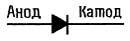
Fig. 1.66. A diode.
The current-voltage characteristic of a diode is shown in Fig. 1.67. (Following our usual approach, we will not go into the physics underlying this element's operation.)
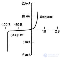
Fig. 1.67. Current-voltage characteristic of a diode.
[[s|diodecurve]]
In the schematic symbol, the direction of the diode's arrow (which marks the element's anode) coincides with the direction of current flow. For example, if a current of 10 mA flows through the diode from anode to cathode, the anode is 0.5 V more positive than the cathode; this voltage difference is called the "forward voltage of the diode." The reverse current for general-purpose diodes is measured in nanoamps (note the different scale on the horizontal axis for forward versus reverse current), and it can generally be disregarded until the voltage across the diode reaches the breakdown voltage (also called the peak inverse voltage). For general-purpose diodes such as the 1N914, the breakdown voltage is typically 75 V. (As a rule, the voltage applied to a diode is kept below the level that could cause breakdown, the previously mentioned Zener diode being the exception.) Most often, the voltage drop across a diode due to forward current through it is between 0.5 and 0.8 V. This voltage drop can be neglected, in which case the diode can be treated as a conductor that passes current in only one direction.
Other key characteristics that distinguish existing diode types from one another include: maximum forward current, capacitance, leakage current, and reverse recovery time (see Table 1.1, which lists the characteristics of several diode types).
Before starting to examine circuits containing diodes, let us note two points: 1) a diode does not have resistance in the sense defined above (it does not obey Ohm's law); 2) a circuit containing diodes cannot be replaced by an equivalent circuit.
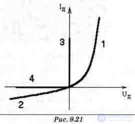
When analyzing circuits with real elements, in particular diodes, one must account for the nonlinearity of their characteristics, which also affects the calculation method used for such circuits. Let us consider the simplest methods for analyzing nonlinear circuits, used to solve the problems presented in this and subsequent chapters. Current-voltage characteristic of a diode. Analysis of the physical processes in a diode yields an expression for its I-V characteristic in exponential form:
 (9.10)
where Is is the saturation current, φT is the thermal potential, and Id, Ud are the diode current and the voltage across it, respectively. This is the simplest case of specifying the diode's I-V characteristic in analytical form. The diode's characteristic can also be measured experimentally point by point, as was done in section 9.1. In that case the characteristic is given in tabular form. Finally, the I-V characteristic can be presented in graphical form, which is quite often used to present typical characteristics in reference data. The diode's I-V characteristic in graphical form is shown in Fig. 9.21.
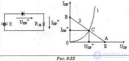
This method is based on the direct use of the diode's I-V characteristic given in graphical form. The graphical method is most suitable when the circuit contains only one diode. In that case, the circuit can be split into two parts: a linear non-ideal voltage or current source (an active two-terminal network) and a nonlinear (passive) two-terminal network, and the equivalent-source method can be used for the calculation. The simplest circuit. Fig. 9.22 shows the simplest circuit for such an analysis. The diode current Id and the voltage Ud across it are related by the following equations:

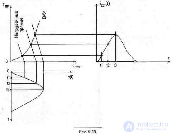
Equation (9.12) describes the diode's I-V characteristic, given in graphical form in Fig. 9.22 (curve 1). Equation (9.11) reflects the load characteristic of the non-ideal EMF source, often called the load line (the slanted line 2 in Fig. 9.22). The load line intersects the voltage axis at point A, cutting off on that axis a segment OA numerically equal to the open-circuit voltage E of the power supply. The load line intersects the current axis at point B, cutting off on that axis a segment 0B numerically equal to the circuit's maximum current E/R. The diode's I-V characteristic and the load line intersect at point C. This point is the graphical solution of the system of equations (9.11), (9.12). The coordinates I*fwd and U*fwd of point C are the desired diode current and voltage, respectively. The supply voltage can have any waveform (for example, sinusoidal). Constructing the time-domain diagram of the diode current for this case is shown in Fig. 9.23. For each instant of time (t1, t2, t3, etc.) one must find the instantaneous values of the supply voltage e(t) and draw the corresponding load line. The points where the load lines intersect the diode's I-V characteristic then determine the instantaneous values of the diode current at the instants t1, t2, t3.
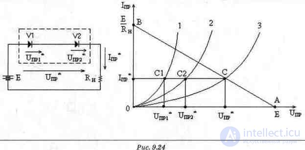
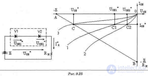
With several diodes connected in series, in parallel, or in a mixed configuration in a circuit, they can be replaced by a single nonlinear two-terminal network, after which the problem is reduced to the previous case. Let us consider this approach for various diode connection configurations. Series connection of diodes. Suppose two diodes are connected in series in a circuit, as shown in Fig. 9.24. The forward branches of the I-V characteristics of diodes V1 and V2 are shown in Fig. 9.24 by curves 1 and 2, respectively. Two series-connected diodes can be represented as a single equivalent nonlinear two-terminal network, for example an equivalent diode. Since the voltage Ufwd across this equivalent diode equals the sum of the voltage Ufwd1 of diode V1 and the voltage Ufwd2 of diode V2, constructing the equivalent diode's I-V characteristic requires adding the individual diodes' I-V characteristics (curves 1 and 2 in Fig. 9.24) with respect to voltage. This yields curve 3 (Fig. 9.24). Now the problem is reduced to the previous case. One must draw the load line AB and find its intersection with the equivalent diode's I-V characteristic. These lines intersect at point C with coordinates I*fwd and U*fwd. Knowing the current, the voltages U*fwd1 and U*fwd2 can be found from the diodes' I-V characteristics. In the example considered, the diodes are forward-biased. Let us consider the same circuit under reverse bias (Fig. 9.25). The reverse branches of the I-V characteristics of diodes V1 and V2 are shown in Fig. 9.25 by curves 1 and 2, respectively. By analogy with the case considered above, the diodes' I-V characteristics must be added with respect to voltage. This yields curve 3 (Fig. 9.25). The point C where the resulting I-V characteristic intersects the load line gives the diodes' reverse current I*rev and reverse voltage U*rev. The intersection of a line parallel to the voltage axis passing through point C with the diodes' characteristics gives the voltages across the diodes U*rev1 and U*rev2. Note that with diodes connected in series, the reverse voltages across them turn out to be unequal. The reason lies in the non-identical reverse branches of the diodes' I-V characteristics. To equalize the reverse voltages across the diodes, additional elements must be introduced into the circuit (for example, equalizing resistors connected in parallel with the diodes).
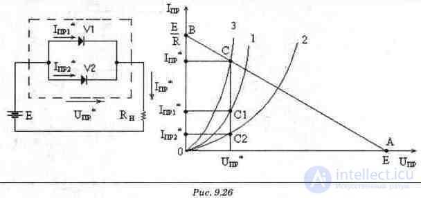
Let us consider an analogous approach for diodes connected in parallel (Fig. 9.26). Two parallel-connected diodes can be regarded as a single equivalent nonlinear two-terminal network, for example an equivalent diode. Since the current Ifwd of this equivalent diode equals the sum of the current Ifwd1 of diode V1 and the current Ifwd2 of diode V2, constructing the equivalent diode's I-V characteristic requires adding the individual diodes' I-V characteristics (branches 1 and 2 in Fig. 9.26) with respect to current. This yields curve 3 in Fig. 9.26. Now the problem is reduced to the one solved earlier. One must draw the load line AB and find its intersection with the equivalent diode's I-V characteristic. These lines intersect at point C. As a result we obtain the voltage U*fwd, which is the same for both diodes V1 and V2. Knowing this voltage, the desired currents I*fwd1 and I*fwd2 can be found from the diodes' I-V characteristics. Note that with diodes connected in parallel, their currents turn out to be unequal. The reason for this is the non-identical forward branches of the diodes' I-V characteristics. To equalize the currents, additional elements must be introduced into the circuit (for example, an equalizing resistor connected in series with each diode).
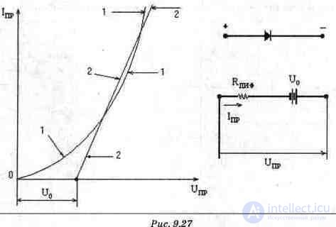
The graphical-analytical method involves two stages of solution. The first consists of approximating the graphically given I-V characteristic with an analytical expression, and the second consists of solving the systems of nonlinear equations set up from Kirchhoff's laws using this expression. If, for example, equation (9.10) were used as the second equation in the system of equations (9.11), (9.12), the system would become transcendental and a solution could not be obtained in analytical form. The most common form of approximation is linearization of the I-V characteristic. In this case, the diode is replaced by a model made up of the simplest linear elements. These models differ for the forward and reverse branches of the I-V characteristic. Fig. 9.27 shows the forward branch of the diode's I-V characteristic (line 1) and the straight-line segment 2 that approximates this branch. The linear-approximation equation has the form: Ud = Rdiff.fwd Id + U0, (9.13) where Rdiff.fwd is the diode's differential resistance under forward bias, and U0 is the threshold voltage. To determine the value of Rdiff.fwd, one must select two arbitrary points on the approximating line (line 2 in Fig. 9.27) (one of them may lie on the voltage axis). For these points, the voltage difference and the current difference must be found, and then the first difference divided by the second. This is the desired value. The forward-bias model of the diode, consisting of an ideal EMF source and a resistance connected in series, is also shown in Fig. 9.27. Fig. 9.28 shows the reverse branch of the diode's I-V characteristic (curve 1) and the straight-line segment 2 that approximates this branch. The equation for this linear approximation has the form:
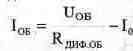 (9.14)
where Rdiff.rev is the diode's dynamic resistance under reverse bias, and I0 is the threshold current. The value of Rdiff.rev is determined the same way as the value of Rdiff.fwd. Below, the forward and reverse differential resistances of the diode, Rdiff.fwd and Rdiff.rev, will be denoted
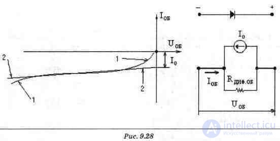
identically as Rdiff, distinguishing between the two notations only where the text requires it. The diode's I-V characteristic under reverse bias is described by expression (9.14). This same expression holds for the two-terminal network shown in Fig. 9.28. Therefore, replacing the diode with this two-terminal network is equivalent. Since the diode's I-V characteristic now has two different analytical expressions and two models (for the forward and reverse portions of the characteristic), it is necessary to determine which one to use. To do this, one must first determine which state (forward or reverse) the diode is in within the original circuit. In relatively simple circuits, the diode's state is not in doubt. In more complex circuits, after completing the calculation, the initial assumption about the state of each diode must be checked. If a diode was initially assumed to operate under forward (reverse) bias, but the calculation yields a negative (positive) current for it, then the assumption about the diode's state is incorrect. A different expression for the diode's I-V characteristic (and a different model) must be used, and the calculation repeated. The expressions obtained, (9.13) and (9.14), can be used to solve specific problems. If the forward voltage drop across an open diode is negligibly small compared to the voltages across the other elements of the circuit, the diode's real forward branch 1 of the I-V characteristic in Fig. 9.21 can be replaced by the vertical straight segment 3. In this case, when calculating the circuit, the diode's terminals (anode and cathode) can be considered short-circuited. If the reverse current of a closed diode is negligibly small compared to the currents through the other elements of the circuit, the diode's real reverse branch 2 of the I-V characteristic can be replaced by the horizontal segment 4. In this case, when calculating the circuit, the branch containing the diode can be considered open. Clearly, both ideal models are limiting special cases of linearizing the characteristics. In that case, solving problems is trivial, and such cases are not considered here. The simplest circuit with one diode (Fig. 9.22), taking into account approximation (9.13), is described by the following system of equations:

Solving this system gives the expression for the diode current:
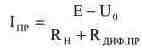 (9.17)
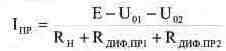
Series connection of diodes. A circuit with two series-connected diodes under forward connection (Fig. 9.24) is described by the system of equations:

where Rdiff.fwd1, Rdiff.fwd2 are the differential resistances of diodes V1, V2 under forward bias, and U01, U02 are the threshold voltages of diodes V1, V2. The equivalent circuit corresponding to this case is shown in Fig. 9.29. The diode current is given by the expression:
 (9.21)
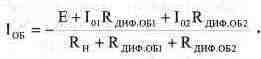
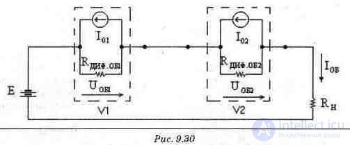
A circuit with two series-connected diodes under reverse bias (see Fig. 9.25), taking into account approximation (9.14), is described by the system of equations:

where Rdiff.rev1, Rdiff.rev2 are the differential resistances of diodes V1, V2 under reverse bias, and I01, I02 are the threshold currents of diodes V1, V2. The equivalent circuit corresponding to this case is shown in Fig. 9.30. The diode current is given by the expression:
 (9.25)
The current Irev is negative, since a reverse voltage is applied to the diodes.
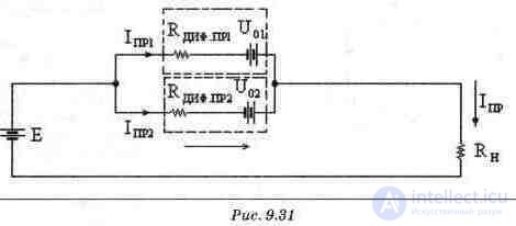
Parallel connection of diodes. A circuit with two parallel-connected diodes (see Fig. 9.26), taking into account approximation (9.13), is replaced by the circuit in Fig. 9.31 and is described by the system of equations:
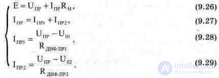
The voltage across the diodes is determined, using the node-potential method, by the expression:
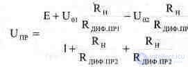 (9.30)
The currents of diodes V1, V2 can be determined by substituting (9.30) into the expressions for the currents (9.28), (9.29). Which of the methods considered is preferable depends on the conditions of the specific problem.
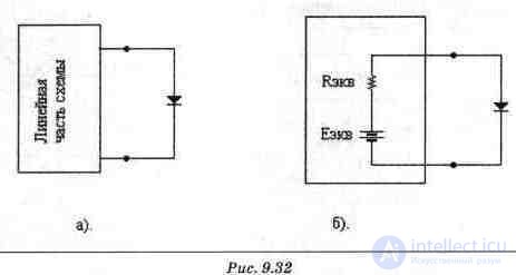
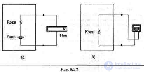
The single-diode circuits offered in this section (files c9_080...c9_111) contain a linear part with a more complex structure. To use the graphical method, the linear part of the circuit must first be replaced by an equivalent source. Let us consider the procedure for this transformation. Suppose the circuit contains only one nonlinear element, for example a diode. Let us extract this diode from the whole circuit, as shown in Fig. 9.32a. The remaining linear part of the circuit can be represented as an equivalent active two-terminal network, shown in Fig. 9.32b. This two-terminal network consists of two elements: an equivalent EMF source Eeq and an equivalent resistor Req (see section 2.1, the part dealing with non-ideal voltage sources). The value of Eeq is easy to measure under open-circuit conditions, by connecting a voltmeter in place of the diode. The measured voltage equals the desired value Eeq. To determine the value of Req, one could measure the short-circuit current of the two-terminal network and then divide Eeq by this current. This approach is sometimes used when experimentally determining the parameters of the equivalent two-terminal network. When calculating Req, it is more convenient to set Eeq = 0 and determine the resistance of the two-terminal network as seen from its terminals. When determining the equivalent resistance, the terminals of EMF sources in the original circuit must be short-circuited, and branches containing current sources must be opened. The same must be done in the actual circuit when measuring resistance. In the measurement circuit shown in Fig. 9.33b, the terminals of the EMF source are short-circuited, and a multimeter set to ohmmeter mode is connected to the two-terminal network's terminals in place of the diode. Calculating circuits with several diodes. When calculating the circuits given in files c9_120...c9_137, the diodes must be replaced by equivalent circuits. This substitution yields a linear calculation circuit. The currents and voltages of the diodes can be determined using methods for analyzing linear circuits. After calculating the circuit, the initial assumptions about the state of each diode (forward or reverse bias) must be checked. The calculation may show that the current of a diode replaced by its equivalent circuit for forward connection turns out to be negative. This means that the initial assumption about this diode's forward connection was incorrect. That diode must be replaced by its equivalent circuit for reverse bias, and the entire calculation repeated. In these problems, the simplest option — an open circuit — is used as the equivalent circuit for the reverse branch of the I-V characteristic. In experiments with models based on an ideal diode
the reverse current is zero. Another case is also possible: the current of a diode replaced by its equivalent circuit for reverse connection turns out to be positive. This means that the initial assumption about the diode's reverse connection was incorrect. The diode must be replaced by its equivalent circuit for forward bias, and the calculation repeated.
A rectifier converts alternating current into direct current; rectifier circuits are the simplest and most practically useful of all diode circuits (diodes are sometimes even called rectifiers).
The simplest rectifier circuit is shown in Fig. 1.68.
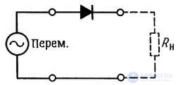
Fig. 1.68. Half-wave rectifier.
The symbol "AC" is used to denote an alternating-voltage source; in electronic circuits it is usually paired with a transformer powered from the AC mains line. For a sinusoidal input voltage significantly greater than the diode's forward voltage (rectifiers typically use silicon diodes, for which the forward voltage is 0.6 V), the output voltage will look as shown in Fig. 1.69. If you recall that a diode is a conductor that passes current in only one direction, it is easy to understand how the rectifier circuit works.
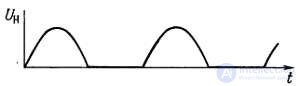
Fig. 1.69.
This circuit is called a half-wave rectifier, since it uses only half of the input signal (half of each period).
Fig. 1.70 shows the circuit of a full-wave rectifier, and Fig. 1.71 shows its output signal.
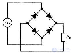
Fig. 1.70. Full-wave bridge rectifier.
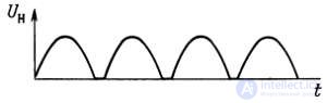
Fig. 1.71.
The graph shows that the input signal is used fully during rectification. On the output voltage graph, intervals with zero voltage can be observed; these are caused by the diodes' forward voltage. In this circuit, two diodes are always connected in series with the input; this should be kept in mind when designing low-voltage power supplies.
The rectified signals obtained in the previous section still cannot be used as direct-current signals. The fact is that they can be considered direct-current signals only in the sense that they do not change polarity. In reality, they contain a substantial amount of "ripple" (periodic voltage oscillations about a constant value), which must be smoothed out to obtain a genuine DC voltage. For this, the rectifier circuit must be supplemented with a low-pass filter (Fig. 1.72).
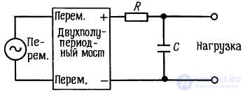
Fig. 1.72.
Generally speaking, the series resistor here is not needed, and it is typically not included in the circuit (if a resistor is present, it has a very small resistance and serves to limit the rectifier's peak current). The fact is that the diodes prevent the discharge current of the capacitors from flowing, so the capacitors act more as energy storage elements than as elements of a classical low-pass filter. The energy stored in a capacitor is given by W = 1/2CU2. If the capacitance C is measured in farads and the voltage U in volts, then the energy W will be measured in joules (in watts times 1 s).
The capacitor is chosen so that the condition RloadC >> 1/f is satisfied (where f is the ripple frequency, 120 Hz in our case). This attenuates the ripple because the capacitor's discharge time constant substantially exceeds the time between recharge events. We will clarify this statement in the next section.
Determining the ripple voltage. It is not hard to estimate the ripple voltage approximately, especially when it is small compared to the DC voltage (Fig. 1.73).
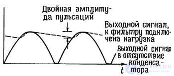
Fig. 1.73. Determining a source's ripple voltage.
The load causes the capacitor to discharge, which happens in the interval between cycles (or half-cycles, for full-wave rectification) of the output signal. If we assume that the current through the load remains constant (which holds for small ripple), then ΔU = (I/C)Δt (recall that I = C(dU/dt)). Substituting the value 1/f (or 1/2f for full-wave rectification) for Δt (this substitution is valid, since the capacitor begins recharging again in less than half a cycle), we get
ΔU = Iload/fC
(half-wave rectification),
ΔU = Iload/2fC
(full-wave rectification).
(Our teaching experience tells us that students love to memorize these equations! An informal survey conducted by the authors showed that of every two engineers surveyed, two do not remember these equations. So don't waste effort on pointless memorization — instead, learn how to derive these relationships.)
If you use the exponential function that describes the change in voltage across a capacitor as it discharges, the result you get will be incorrect, for the following reasons:
1. Capacitor discharge follows an exponential law only if the load is resistive; in most cases it is not. A voltage regulator is often installed at the rectifier's output to keep the rectified voltage constant — it acts as a load through which a constant current flows.
2. Power supplies typically use capacitors with a tolerance of 20% or more. When designing circuits, one should account for the spread in component parameters and, to be safe, calculate for the least favorable combination of values. In that case, if we assume that the capacitor initially discharges according to a linear law, the approximation will be quite accurate, especially when the ripple is small. The inaccuracies of the approximation merely amount to a certain margin of safety — they show up as an overestimate of the calculated ripple voltage compared with its true value.
Exercise 1.27. Design a full-wave rectifier circuit that provides an output DC voltage with an amplitude of 10 V. The ripple voltage must not exceed 0.1 V (peak-to-peak). The load current is 10 mA. Choose an appropriate AC input voltage, taking into account that the voltage drop across the diode is 0.6 V. Make sure to use the correct ripple frequency in your calculation.
Full-wave bridge circuit. Fig. 1.74 shows the circuit of a DC power supply with the bridge rectifier we just discussed.
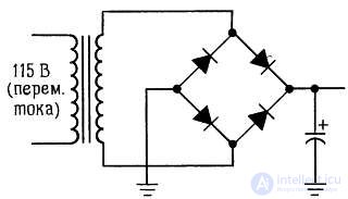
Fig. 1.74. Bridge rectifier circuit. The polarity mark and the arc-shaped electrode denote a polarized capacitor; charging it with the opposite polarity is not permitted.
Industry manufactures bridge circuits in the form of functional modules. Small bridge modules are rated for a maximum current of 1 A and a breakdown voltage of 100 to 600 V, sometimes up to 1000 V. For larger bridge rectifiers, the maximum current is 25 A and higher. Table 6.4 lists the parameters of several types of such modules.
Full-wave single-phase rectifier. The circuit of a full-wave single-phase rectifier is shown in Fig. 1.75.
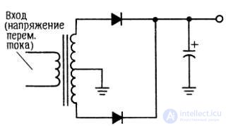
Fig. 1.75. Full-wave rectifier based on a center-tapped transformer.
Here the output voltage is half that of the bridge-rectifier circuit. The full-wave single-phase rectifier circuit is not efficient in terms of transformer utilization, since each half of the secondary winding is used for only one half-cycle. As a result, the current in the winding during that interval is twice that in a simple full-wave circuit. According to Ohm's law, winding heating is proportional to the product I2R, so with the time halved, the heating will be four times greater, or on average greater, compared with an equivalent full-wave circuit.
The transformer for this circuit should be chosen so that its maximum current rating is 1.4 (i.e., √2) times greater than that of a transformer for the bridge circuit; otherwise such a rectifier will be more expensive and bulkier than a bridge rectifier.
Exercise 1.28. This exercise will help you understand the mechanism of winding heating proportional to I2R, and see where the drawback of the single-phase rectifier shows up. What minimum current rating should a fuse have so that it can carry a current that varies according to the graph shown in Fig. 1.76 and has an average amplitude of 1 A?
Hint: a fuse "blows" when the current flowing through the circuit exceeds the fuse's rated current. In that case, the metal conductor inside the fuse melts (its heating temperature is proportional to I2R).
Assume that in our case the thermal time constant of the fuse is much greater than the period of the square-wave oscillations, i.e., the fuse responds to the value of I2 averaged over several periods of the input signal.
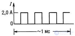
Fig. 1.76.
Splitting the supply voltage. A widely used circuit is the single-phase full-wave bridge rectifier shown in Fig. 1.77. It allows the supply voltage to be split (producing equal positive and negative output voltages).
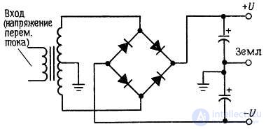
Fig. 1.77. Generating a split (bipolar) supply voltage.
This circuit is efficient, since both halves of the secondary winding are used in each half-cycle of the input signal. Voltage-multiplying rectifiers. The circuit shown in Fig. 1.78 is called a voltage doubler.
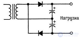
Fig. 1.78. Voltage doubler.
To understand how this circuit works, imagine that it consists of two rectifiers connected in series. In fact this circuit is a full-wave rectifier, since it operates during each half-cycle of the input signal — the ripple frequency is twice the frequency of the mains supply (for a mains frequency of 60 Hz, as in the US, the ripple frequency is 120 Hz). Variants of this circuit allow the voltage to be increased by a factor of 3, 4, or more.
Fig. 1.79 shows rectifier circuits that provide a 2x, 3x, and 4x voltage increase, in which one end of the transformer winding is grounded.
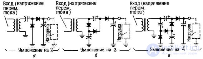
Fig. 1.79. Voltage-multiplier circuits; a floating-voltage source is not required in the circuits shown.
By increasing the capacitance of the capacitor, the voltage ripple can be reduced to the required level. This way of dealing with ripple has two drawbacks:
1. Capacitors of the needed capacitance may turn out to be unacceptably bulky and expensive.
2. Even when the ripple has been reduced to a negligible level, fluctuations in the output voltage are still observed, caused by other reasons — for example, changes in the mains input voltage lead to fluctuations in the DC output voltage. In addition, a change in the output voltage can be caused by a change in the load current, since the transformer, diode, and other elements have a finite internal resistance. In other words, for the equivalent circuit of a DC power supply, the relation R > 0 holds.
A more correct approach to designing a power supply is to use a capacitor to reduce the ripple to some level (for example, to about 10% of the DC voltage), and then use a feedback circuit to eliminate the remaining ripple. Such a circuit contains a controlled resistor (a transistor) connected in series with the circuit's output, by means of which the output voltage level is kept constant (Fig. 1.80).
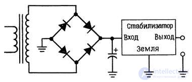
Fig. 1.80. DC voltage regulator.
Such voltage regulators are used almost everywhere as power supplies for electronic circuits. Nowadays industry produces voltage regulators as complete, ready-to-use modules. Based on a voltage regulator, one can build a power supply that is convenient to work with, immune to any hazards (short circuits, overheating, etc.), and whose characteristics satisfy the highest requirements placed on a voltage source (for example, the internal resistance of such a source is measured in milliohms).
We will look at DC power supplies with voltage regulators in Chapter 6.
Signal rectification. Besides the cases considered above, there are situations where a signal must have only one polarity. If the input signal is not sinusoidal, it is not customary to speak of "rectifying" it, although the rectification process still applies to it. For example, suppose a sequence of pulses is needed, coinciding with the rising edges of a square-wave signal. The simplest approach is to differentiate the square-wave signal and then rectify it (Fig. 1.81).
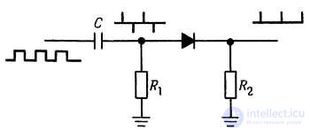
Fig. 1.81.
It should always be kept in mind that a diode's forward voltage is approximately 0.6 V. At the output of our circuit, for example, a signal will only be obtained if the peak-to-peak amplitude of the square-wave input signal is at least 0.6 V. This condition places certain constraints on the circuit design, but there are known techniques for overcoming them. For example, one can use a Schottky diode, whose forward voltage is around 0.25 V (one could also use a so-called back diode with zero forward voltage, but its use is limited because it has a low breakdown voltage). One can also use the circuit shown in Fig. 1.82.
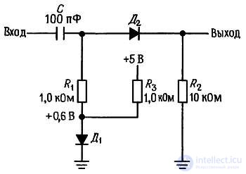
Fig. 1.82. Compensating for a diode's forward voltage in a diode clipper circuit.
The forward voltage across diode D2 is compensated by diode D1, which provides a bias of 0.6 V. This bias sets the conduction threshold for D2. Generating the bias with diode D1 (rather than, say, with a voltage divider) has the following advantages: there is no need to adjust the bias level, since the circuit provides nearly ideal compensation; and changes in the diodes' forward voltage (due, for example, to temperature changes) are compensated and do not affect the circuit's operation. Later on we will repeatedly encounter compensation of forward-voltage changes using a matched pair of diodes, transistors, or field-effect transistors — this technique is very effective and simple to implement.
Diode gates. Another application of diodes is based on their ability to pass through the greater of two voltages while having no effect on the smaller one. Circuits that exploit this property belong to the family of logic circuits. Consider a circuit with a backup battery — used in devices that must operate continuously even during power outages (for example, precision electronic clocks). The circuit shown in Fig. 1.83 includes just such a battery. When there is no power failure, the battery does not operate; when a failure occurs, power to the circuit begins to come from the battery, and there is no interruption in the power supply.
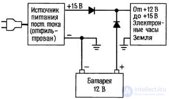
Fig. 1.83. Diode OR gate with a backup battery.
Exercise 1.29. Modify the circuit so that the battery is charged from the DC source (when power is present, of course) with a current of 10 mA (such a circuit is needed to keep the battery topped up).
Diode limiters. In cases where it is necessary to limit the range of variation of a signal, for example a voltage, the circuit shown in Fig. 1.84 can be used.
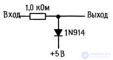
Fig. 1.84. Diode voltage limiter.
Thanks to the diode, the output voltage cannot exceed +5.6 V, while the presence of the diode has no effect on smaller voltage values (including negative ones); the only condition is that the negative input voltage must not reach the breakdown voltage (for example, for a 1N914-type diode this value is —70 V). All circuits in the CMOS digital logic family use input diode limiters. They protect these sensitive circuits from being destroyed by electrostatic discharge.
Exercise 1.30. Design a symmetric limiter circuit that sets the signal's range of variation from —5.6 to +5.6 V.
A reference voltage can be fed to the limiter from a voltage divider (Fig. 1.85).
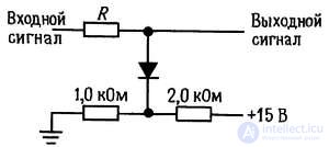
Fig. 1.85.
If the voltage divider is replaced by its equivalent circuit, the original circuit is transformed into the form shown in Fig. 1.86.
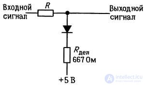
Fig. 1.86.
Analyzing the transformed circuit, one can conclude that the impedance seen at the divider's output (Rdiv) must be small compared with the resistance R. When the diode is open (the input voltage exceeds the clipping voltage), the output voltage matches the voltage taken from the divider, with the divider's lower arm represented by its equivalent resistance (Fig. 1.87).
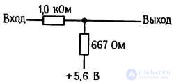
Fig. 1.87.
Consequently, for the given circuit parameters, the output voltage for a triangular input signal will have the form shown in Fig. 1.88.
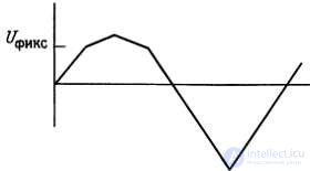
Fig. 1.88.
The difficulty here arises from the fact that the voltage divider does not provide a firmly fixed reference-voltage value. A well-fixed reference signal does not "drift," which means that the source of such a voltage has a low impedance (meaning the equivalent impedance).
Fig. 1.85 shows a simple way to "fix" the limiter circuit, at least for high-frequency signals — for this, a bypass capacitor must be connected across the 1 kΩ resistor.
For example, a 15 μF capacitor with one grounded terminal reduces the impedance seen at the divider's input to below 10 Ω at frequencies above 1 kHz. (A capacitor can similarly be connected to D1, as shown in Fig. 1.82.) Needless to say, this technique's effectiveness decreases as the frequency decreases, and for direct current it is simply useless.
In practice, a low reference source impedance is achieved by using a transistor or an operational amplifier. This approach is certainly better than using very-low-resistance resistors, since it doesn't require large currents to be drawn and provides impedance values on the order of a few ohms or less.
It should be noted that other limiter circuits using operational amplifiers are also known. We'll discuss these circuits in Chapter 4.
An interesting example is the use of a limiter to restore the DC component of a signal in the case of AC (capacitive) coupling. The idea is illustrated in Fig. 1.89. Such techniques must be used in circuits whose inputs behave like diodes (for example, transistors with a grounded emitter), since otherwise, with capacitive coupling present, the signal simply disappears.
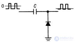
Fig. 1.89. Restoring the DC component of a signal.
Two-sided limiter. Another limiter is shown in Fig. 1.90.
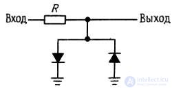
Fig. 1.90. Diode limiter.
This circuit limits the "swing" of the output signal and makes it equal to the voltage drop across the diode, i.e., approximately 0.6 V. This may seem like a very small value, but if the next stage of the circuit is an amplifier with a high voltage gain, the input signal to it must always be only slightly greater than 0 V, or else the amplifier will go into "saturation" (for example, if the stage gain is 1000 and the supply voltage is ±15 V, the input signal must not exceed a range of ±15 mV). The circuit described is often used to protect the input of a high-gain amplifier.
Diodes as nonlinear elements. We get a fairly good approximation if we assume that the current through a diode is proportional to an exponential function of the voltage across it at a given temperature (the exact relationship between current and voltage is given in Section 2.10). Because of this, a diode can be used to obtain an output voltage proportional to the logarithm of the current (Fig. 1.91).
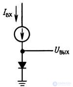
Fig. 1.91. Logarithmic converter: the circuit idea is based on the diode's nonlinear current-voltage characteristic.
Since the voltage U deviates only slightly from 0.6 V (due to fluctuations in the input current), the input current can be set using a resistor, provided that the input voltage is significantly greater than the voltage drop across the diode (Fig. 1.92).
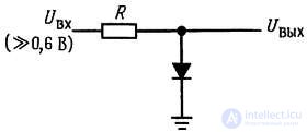
Fig. 1.92.
In practice, it is sometimes desirable for the output voltage to include a 0.6 V offset caused by the diode's voltage drop. In addition, it is desirable that the circuit not respond to temperature changes. These requirements can be satisfied by the diode compensation method (Fig. 1.93).
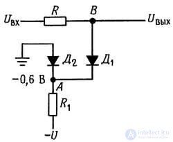
Fig. 1.93. Compensating for the diode voltage drop in a logarithmic converter.
Resistor R1 turns on diode D2 and creates a voltage of -0.6 V at point A. The potential at point B is close to ground potential (in which case the current Iin is strictly proportional to the voltage Uin). If two identical diodes are under identical temperature conditions, the voltages across them fully compensate each other, except of course for the difference caused by the input current flowing through diode D1, which determines the output voltage. For this circuit, resistor R1 should be chosen so that the current through diode D2 is significantly greater than the maximum input current. Under this condition, diode D2 will remain turned on.
In the chapter devoted to operational amplifiers, we'll look at more sophisticated logarithmic converter circuits and more precise temperature compensation methods. These allow high conversion accuracy to be achieved—the error amounts to only a few percent over six or more decades of input current variation. But before tackling such circuits, it's necessary first to study the characteristics of diodes, transistors, and operational amplifiers. This section serves merely as an introduction to that study.
What happens if you open a switch controlling current through an inductor? An inductor, as is well known, has the following property: U = L(dI/dt), from which it follows that current cannot be switched off instantaneously, since this would produce an infinite voltage across the inductor. In reality, the voltage across the inductor rises sharply and continues to increase until current appears. Electronic devices that control inductive loads may not survive such a voltage spike, especially components that undergo "breakdown" at certain voltage values. Let's consider the circuit shown in Fig. 1.94.
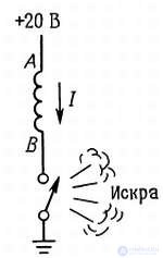
Fig. 1.94. Inductive "kick."
In the initial state, the switch is closed and current flows through the inductor (which could be, for example, a relay winding). When the switch is opened, the inductor "tries" to maintain a current between points A and B flowing in the same direction as when the switch was closed. This means that the potential at point B becomes more positive than the potential at point A. In our case, the potential difference can reach 1000 V before an electric arc forms across the switch, closing the circuit. This shortens the switch's service life and generates pulse interference that can affect the operation of nearby circuits. If we imagine a transistor being used as the switch instead, its service life doesn't just shorten—it drops to zero!
To avoid such trouble, it's best to connect a diode across the inductor, as shown in Fig. 1.95.
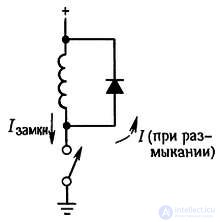
Fig. 1.95. Blocking the inductive kick.
When the switch is closed, the diode is reverse-biased (due to the DC voltage drop across the coil winding). When the switch is opened, the diode turns on and the potential at the switch contact rises above the positive supply voltage by an amount equal to the voltage drop across the diode. The diode must be chosen so that it can withstand an initial current equal to the steady-state current flowing through the inductor; for example, a 1N4004-type diode would work.
The only drawback of this circuit is that it prolongs the decay of the current flowing through the coil, since the rate of change of this current is proportional to the voltage across the inductor. In cases where the current must decay quickly (for example, high-speed impact printers, high-speed relays, etc.), a better result can be obtained by connecting a resistor to the coil, chosen so that the value of Ui + IR does not exceed the maximum allowable voltage across the switch. (The fastest decay for a given maximum voltage can be obtained by connecting a Zener diode across the inductor, which provides decay following a linear rather than an exponential law.)
Diode protection cannot be used for AC circuits containing inductors (transformers, AC relays), since the diode would be turned on during those half-cycles of the signal when the switch is closed. In such cases, it's recommended to use what's called an RC snubber network (Fig. 1.96).
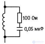
Fig. 1.96. RC "snubber" for suppressing an inductive kick.
The R and C values shown in the circuit are typical for small inductive loads connected to AC power lines. A snubber of this type should be included in all devices operating from AC power line voltages, since a transformer is itself an inductive load. A metal-oxide varistor can also be used for protection. This is an inexpensive component, similar in appearance to a ceramic capacitor, but with electrical characteristics resembling those of a bidirectional Zener diode. It can be used over a voltage range of 10 to 1000 V for currents reaching thousands of amperes (see Section 6.11 and Table 6.2). Connecting a varistor to the circuit's external terminals not only prevents inductive interference from affecting nearby devices but also suppresses large voltage surges that sometimes occur on the power line and pose a serious threat to equipment.
Diodes can perform switching and digital logic operations. Forward and reverse bias switch the diode between low- and high-resistance states, respectively. In this way, the diode acts as a switch.
Diodes can perform digital logic functions: AND and OR. Diode logic was used in early digital computers. Today it has only limited application. Sometimes it's convenient to build a single logic gate out of several diodes.
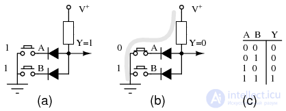
Diode AND gate
A diode AND gate is shown in the figure above. Logic gates have inputs and an output (Y), which is a function of the inputs. The inputs of the gate can be at a high logic level (logic 1), say, 10 V, or a low logic level, 0 V (logic 0). In the figure, the logic levels are generated by pushbuttons. If a button is released, the input signal is high (1). If a button is pressed, it connects the diode's cathode to ground, corresponding to a low level (0). The output depends on the combination of inputs A and B. The inputs and output are usually recorded in a "truth table" (figure (c)) to describe the gate's logic. In figure (a), both inputs are at a high logic level (1). This is recorded in the last row of the truth table (c). The output, Y, is at a high logic level (1) due to the voltage V+ at the top terminal of the resistor. It is unaffected by the open switches. In figure (b), switch A pulls the cathode of the connected diode to a low level, pulling the output Y down to a low level (0.7 V) as well. This is recorded in the third row of the truth table. The second row of the truth table describes the output with the switches in states opposite to those shown in figure (b). Switch B pulls its diode and the output down to a low level. The first row of the truth table records Output=0 for a low logic level (0) on both inputs. This truth table describes the AND logic function. In summary: a high logic level on both inputs (both A and B) produces a high logic level (1) at the output.
The figure below shows a two-input OR gate built from a pair of diodes. If both inputs are at a low logic level (figure (a)), simulated by both switches in the "down" (open) position, the output Y is pulled to a low level by the resistor. This logic zero is recorded in the first row of the truth table (c). If the first input is at a high logic level, as shown in figure (b), or the other input is high, or both inputs are high, the diode(s) conduct, pulling the output Y to a high logic level as well.
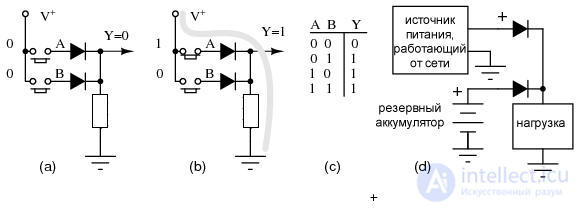
OR gate: (a) First row of the truth table. (b) Third row of the truth table. (d) An OR gate with a mains-powered supply and a backup battery on the inputs.
Using the OR gate circuit, a backup battery can be connected together with a mains-powered DC source to power a load even when the mains voltage is lost. When AC mains voltage is present, the load is powered by the mains-powered source, assuming its output voltage is greater than the battery voltage. If the mains voltage is lost, the voltage from the mains-powered source drops to 0 V, and the load is then powered by the battery. The diodes must be connected in series with the power sources to prevent current from flowing from the mains-powered source through the battery, which could cause the battery to be overcharged while mains power is present. Does your computer retain its BIOS settings after a power outage? Do mains-powered clocks retain their settings and time after a power outage?
Diodes can switch analog signals. A reverse-biased diode is, in effect, an open circuit. A forward-biased diode is a low-resistance conductor. The only problem is separating the AC signal being switched from the DC control signal. The circuit in the figure below shows a parallel resonant circuit: the tank inductor is connected in parallel with one (or more) tank capacitors. This parallel LC tank circuit could be a preselector filter in a radio receiver. It could determine the frequency of an oscillator (not shown). The digital control lines could be driven through a microprocessor interface.
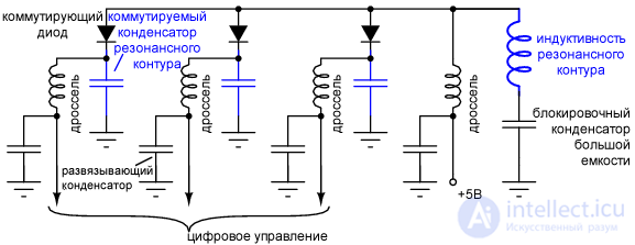
Diode switch: a digital control signal (logic zero) selects a tank capacitor by forward-biasing the switching diode
A large DC-blocking capacitor connects the tank inductor to ground for AC while blocking DC. It must have low reactance compared to the reactances of the parallel LC tank circuit. It prevents the DC voltage at the anode from being shorted to ground through the tank inductor. The switched tank capacitor is selected by pulling the corresponding digital control input to a low logic level. This forward-biases the switching diode. DC current flows from the +5V point through the radio-frequency choke (RFC), the switching diode, and to ground through the digital control line. The purpose of the radio-frequency choke (RFC) in the +5V line is to prevent AC current from flowing into the +5V source. The choke in the digital control line must prevent AC current from flowing out through the external control line. The bypass capacitor shunts the small AC current flowing through the radio-frequency choke to ground, bypassing the external digital control line.
At a high logic level (≥+5V) on all three digital control lines, none of the switched tank capacitors is selected, due to reverse bias on the diodes. Pulling one or more lines to a low logic level selects one or more of the corresponding switched tank capacitors. Since the additional capacitors are connected in parallel with the tank inductor, the resonant frequency decreases
The capacitance of a reverse-biased diode can have an effect in circuits operating at very high frequencies and ultra-high frequencies. In this case, PIN diodes, which have lower parasitic capacitance, can be used for switching.

Comments