
Lecture
The latch-up effect (Latch-up) is a type of short circuit that can occur in an integrated circuit (IC). Specifically, it is the unintentional creation of a low-impedance path between the power rails of a MOSFET circuit, triggering a parasitic structure that disrupts the proper operation of the part, possibly even leading to its destruction due to current overload. A power cycle is required to correct this situation.
Single event latch-up is latch-up caused by a single-event upset, usually from heavy ions or protons from cosmic rays or solar flares.
The parasitic structure is usually equivalent to a thyristor (or SCR), a PNPN structure that acts as PNP and NPN transistors located next to each other. During latch-up, when one of the transistors conducts, the other also begins to conduct. They keep each other in saturation as long as the structure is forward-biased and some current flows through it, which usually means until the power is switched off. The parasitic SCR structure forms as part of a pair of totem-pole PMOS and NMOS transistors in the output gate drivers.
Latch-up need not occur only between the power rails — it can occur anywhere the required parasitic structure exists. A common cause of latch-up is a positive or negative voltage spike on an input or output pin of a digital chip that exceeds the rail voltage by more than a diode drop. Another cause is the supply voltage exceeding its absolute maximum rating, often due to a transient spike in the power supply. This leads to breakdown of an internal junction. This often happens in circuits that use several supply voltages that do not come up in the required sequence at power-on, resulting in voltages on data lines that exceed the input specifications of parts that have not yet reached their rated supply voltage. Latch-up can also be triggered by electrostatic discharge.
High-power microwave interference can also cause latch-up. Another common cause of latch-up is ionizing radiation, which makes it a serious problem in electronic products intended for space (or very high-altitude) applications.
Both CMOS and TTL integrated circuits are more susceptible to latch-up at higher temperatures.
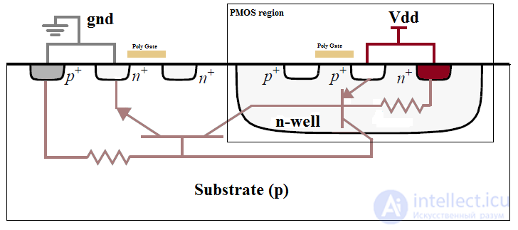
Integrated bipolar junction transistors in CMOS technology
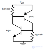
All CMOS chips have latch-up paths, but there are several design techniques that reduce susceptibility to latch-up
In CMOS technology there are a number of transistors with an internal bipolar junction. In CMOS processes these transistors can create problems when the combination of the n-well/p-well and the substrate results in the formation of parasitic npnp structures. Triggering of these thyristor-like devices causes a short circuit between the Vdd and GND lines, which usually leads to destruction of the chip or a system failure that can only be cleared by switching off the power.
Let us consider the structure with n-wells in the first figure. The npnp structure is formed by the NMOS source, the p-substrate, the n-well, and the PMOS source. The equivalent circuit is also shown. When one of the two bipolar transistors is forward-biased (due to current flowing through the well or the substrate), it feeds the base of the other transistor. This positive feedback increases the current until the circuit fails or burns out.
In 1977, Hughes Aircraft invented the standard technology for preventing latch-up in CMOS devices.
Latch-up-resistant chips can be designed by adding a layer of insulating oxide (called a trench ) that surrounds both the NMOS and PMOS transistors. This disrupts the structure of the parasitic silicon-controlled rectifier (SCR) between these transistors. Such details are important in cases where the correct sequencing of power and signals cannot be guaranteed, for example, in hot-swappable devices .
Devices made from lightly doped epitaxial layers grown on heavily doped substrates are also less prone to latch-up. The heavily doped layer acts as a current sink, where excess minority carriers can recombine quickly. [10]
Most silicon-on-insulator devices are inherently resistant to latch-up. Latch-up is a low-resistance connection between the well and the power-supply rails.
Also, to avoid latch-up, a separate tap connection is provided for each transistor. But this increases the size of the device, so fabs leave the minimum spacing for placing a tap, for example, 10 µm in the 130 nm process.

Comments