
Lecture
Это окончание невероятной информации про электроника .
...
"National Semiconductor," Apple (USA) Macintosh
Block diagram and composition of a microprocessor system
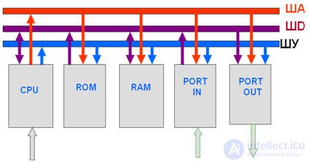
Types of microprocessor buses
Address bus – AB (16);
Data bus – DB (8);
Control bus – CB (10-12) implemented as a set of conductors connecting the main elements of the microprocessor to each other;
CPU- central processing unit
ROM – read-only memory, for storing control programs and a set of initial data for organizing the information processing operation
RAM – random access memory, for storing the changing portion of the data being processed
I/O devices – input/output devices, ports for exchanging data between the microprocessor and the keyboard, monitor, printer, etc.
Internal architecture of a microprocessor
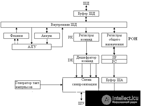
ALU – arithmetic-logic unit, implementing the set of arithmetic and logic functions of the microprocessor.
Clocking and control unit – receives and generates external control signals.
Register set – for temporary storage of instruction codes, data, addresses, and information about the internal state of the microprocessor.
The contents of some internal registers of the microprocessor can be changed, while another part of them is inaccessible to the programmer.
IR – instruction register receives the code of the current instruction from the data bus and holds it for the entire duration of its execution. The instruction register is not accessible to the programmer.
General-purpose registers – for storing data and intermediate results.
Accumulator – if the microprocessor has only a single dedicated register for storing data and intermediate results.
Stack pointer register SP – for storing the address of the last unused stack memory cell (a memory region whose size changes during processing). The stack operates on the "last in, first out" principle.
PC – program counter.
Flag register – the status register or condition-code register, programmatically accessible.
All operations in the microprocessor are initiated by clock pulses from an external clock pulse generator, stabilized by a crystal oscillator.
The clock frequency can be used to judge the microprocessor's speed. The first microprocessors had a speed of 2-4 MHz; modern ones – 3 GHz
Additional resources – coprocessors
• Arithmetic coprocessor;
• Cache memory;
• Microcontroller;
• Graphics microprocessor.
Basic microprocessor instructions
• data transfer instructions (from memory to a register and vice versa, transfer from register to register);
• arithmetic and logic instructions (addition, subtraction, etc., and logic operations AND, OR, NOT, etc.);
• jump instructions from one point in the program to another (conditional jumps);
• instructions for controlling the microprocessor's operation; input-output, stack operations, etc.
Writing, reading, and debugging programs is simplified when instructions are written in a machine-oriented language – assembly or BASIC.
8-bit microprocessors are intended for building microcontrollers based on them – simple microcomputers for use in industry, everyday life, and as control systems
Digital memory devices
Flip-flop-based memory registers
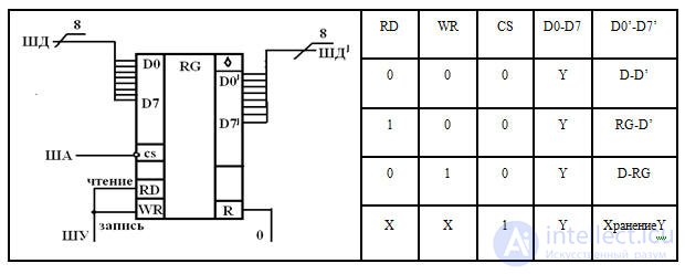
CS - always-active inverted chip-select input.
The RG register stores 8 bits of information.
If 8 registers are used, an 8-byte memory is obtained
On the control bus: "0" - read RD, "1" - write WR
Parallel register
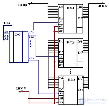
If many registers RG1-RG8 are used, a positional decoder DC is needed to select the register for reading or writing information.
For example: we want to read data from RG1; to do this, a "1" is applied to input RDRG1, and the address selection code for RG1 goes on the address bus, i.e., "0" appears at the decoder's output cs1, while all others are "1".
By combining a decoder and registers in a single IC, a read-only memory chip is obtained.
Such ICs have a single data bus, which is divided by the RD/WR signals, i.e., the data bus is bidirectional.
In processors, the data bus is always 8 wires wide; in computers, 16, 32, 64; modern coprocessors, 96
In memory ICs the number of addresses is 4096, with a 4096×8 configuration; the control bus typically has 10-50 wires
Example 1: an address bus for 64 registers, configuration 64×8
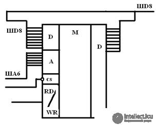
Example 2
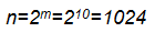
Determine the information capacity n of a memory IC if the number of address inputs m=10
Main characteristics of memory devices
• information capacity;
• speed;
• information retention time.
1. Information capacity N – the number of memory bits in the memory device's storage array;
2. Number of words n – the number of word addresses in the memory device's storage array;
3. Word width m – the number of bits per word in the memory device's storage array;
4. Number of reprogramming cycles Ncy – the number of write-erase cycles for which the memory device remains functional;
5. Steady-state power consumption Pcc;
6. Standby (retention-mode) power consumption Pccs;
7. Retention time tsg .
Static parameters of memory devices
• Supply voltage Ucc
• Supply current Icc
• Standby-mode supply current Iccs
• Standby-mode supply voltage Uccs
• Logic-high voltage Uh
• Logic-low voltage Ul
Dynamic parameters of memory devices:
• chip select time;
• address access time;
• signal access time.
Classification of memory devices:
by functional purpose
• RAM
• ROM
• PROM
• EPROM
• EEPROM
• FLASH
by method of information storage
Static
Bistable cells (transistors), non-destructive read of information; 10,000 cells
Dynamic
Information storage relies on the inertial properties of reactive elements (capacitors) (periodic recharging/refresh is required)
by manufacturing technology
• semiconductor memory devices based on bipolar transistors (TTL, ECL);
• semiconductor memory devices based on insulated-gate field-effect transistors, CMOS;
• charge-coupled semiconductor memory devices;
• devices with an MNOS structure (metal - silicon nitride - Si oxide - semiconductor).
by method of addressing the array of memory elements
• random access, which allow any order of address sequencing;
• sequential access, in which memory elements can only be accessed in order of increasing or decreasing addresses (shift registers)
Random access memory RAM
A digital information storage device combined with control circuits that provide write, storage, and read modes for digital information during its processing.
Static and dynamic RAM
Static RAM
• The basis is a storage array or memory matrix consisting of individual bistable storage cells.
• The cells – flip-flops – contain six MOS field-effect transistors.
• Binary information is stored in a cell until it is replaced by other information or until the supply voltage is removed.
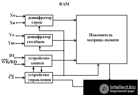
Chip select, row address strobe RAS, column CAS
• A RAM IC with a capacity of 1Kbit contains 1024 flip-flops.
• Address decoding circuits, located inside the RAM chip, select a specific flip-flop each time, as indicated by the signals on the address lines.
Symbol of a static RAM IC (K537RU17)
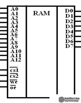
Using RAM solves two tasks:
1. Selecting the specific storage cell into which data will be written or from which it will be read
2. Reading or writing the information
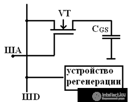
Dynamic RAM
To increase information capacity, dynamic RAM is used, in which information is stored in the form of a charge on corresponding capacitors.
Capacitor capacitance Cstor=0.1 pF, retention time 1ms.
Regeneration (restoration) of the stored information is required with a period no greater than 1ms.
The memory cell is implemented using either bipolar or MOS transistors without a special power source.
Addressing is sequential
Memory cell
• Information is stored in Cgs;
• Power consumption Pcons=50-500mW;
• The entire system operates in switching mode.
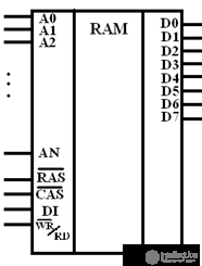
Symbol for dynamic RAM ICs
Read-only memory (ROM)
Types of ROM storage arrays:
• ROM - mask-programmed (memory matrix), programmed at the manufacturing stage.
• PROM - programmable ROMs implemented on the basis of memory cells with fusible nichrome links.
• Series K500 K1500 KR556RT.
• The user programs it electrically, using a programmer for user-multiply-programmable ROMs.
• EPROM - with electrical programming and ultraviolet erasure.
• EEPROM - with electrical programming and electrical erasure.
• SEEPROM (EAPROM) - with electrical programming and selective erasure.
• A common property of ROM ICs is a multi-bit (word-oriented) organization, with reading as the main mode.
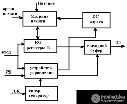
Structure of an electrically-programmed ROM
ROM symbol
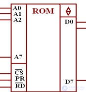
4 address lines give 256 memory cells 
• If a microprocessor system contains several memory modules, a memory map is drawn up, i.e., the address space distribution.
• Address space – the bit width of the address bus.
• Width 16 => 65536 the number of addressable registers or memory cells.
ROM K155RE21-24 (ROM)
• Codes of the letters of the Russian alphabet are stored in RE21
• Codes of the letters of the Latin alphabet are stored in RE22
• Codes of arithmetic signs and digits are stored in RE23
• Codes of additional symbols are stored in RE24
• The set of ICs forms a character generator for 96 characters in a 7×5 format
Problems and examples
DIODES, RECTIFIERS
1. Given: circuit (Fig. 1), U1 = 10 V, U2 = 13 V, U3 = 15 V, U4 = 22 V, R1 = R2 = 1 kOhm. Determine Uout
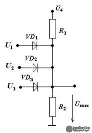
Solution:
When U1 = U2 = U3 = 0, the diodes are closed and the voltage
Uout = U4•R2 / (R1 + R2) = 11 V.
If we connect U1, Uout will not change — the diodes remain closed.
When U2 is connected, Uout becomes 13 V (the diode in the branch with U2 will be open).
When U3 is connected, the diode in that branch opens, and Uout becomes 15 V. The other diodes close.
2. Assuming the diodes are ideal, find the value of the current and voltage for the circuits shown in the diagram.
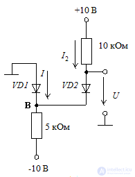
Solution:
For the circuit shown, it is not obvious whether both diodes are in the conducting state. In this case we will assume that the diodes are conducting, carry out the calculations, and then check whether our assumption is correct.
For the circuit, assuming both diodes are conducting, it follows that
UB = 0; U = 0
The current through diode VD2 can be found from the expression
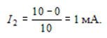
Writing the equation for the currents at node B, we have
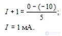
Thus, diode VD1 is in the conducting state, as we initially assumed, and the final results are
I = 1 mA and U = 0 V.
3. Determine the current in the circuit and the voltage across the diodes whose I-V characteristics are shown, if Uin = 2.5 V, Rload = 25 Ohm
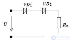
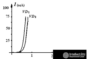
Solution:
we construct the combined I-V characteristic of the diodes and the "inverted" I-V characteristic of the load resistor.
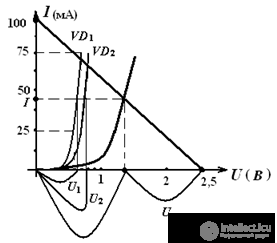
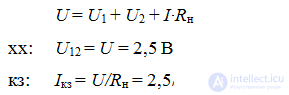
Answer: U1 = 0.6 V, U2 = 0.7 V, Uload = 1.2 V, I = 45 mA
Rectifiers
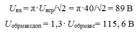
4. In a half-wave rectifier (without a filter), the voltage across the load is Uload,avg = 40 V.
What maximum reverse voltage Urev,max should the semiconductor diode be chosen for?
Solution:
5. In a half-wave rectifier, the voltage on the secondary winding of the transformer is U2 = 150 V. The mains frequency is 50 Hz,
Rload = 2 kOhm.
Determine Uload,avg, Iforward, Iload,avg, Urev,max, and the ripple factor p.
Solution:
Uload,avg =√2•U2/π = 67.36 V
Iload,avg = Uload,avg/ Rload = 67.36 / 2000 = 0.034 A
Iforward = Iload,avg = 0.034 A
Urev,max = √2•U2 = 212 V
p = 1.57
.
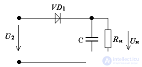
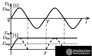
6. In a half-wave rectifier with a capacitive filter, Fig. 21, calculate Uload,avg and Urev,max if Cfilter = ∞, U2 = 150 V, mains frequency 50 Hz,
Rload = 2 kOhm, and plot the rectifier's time diagram.
Solution:
Cfilter = ∞, therefore p = 0
Uload,avg =√2•U2 / (1 + p) = 212 V
Iload,avg = Uload,avg/ Rload = 212 / 2000 = 0.106 A
Iforward = Iload,avg = 0.106 A
Urev,max = 2√2•U2 = 424 V
Time diagram of the rectifier.
7. In a full-wave bridge rectifier circuit with a filter, the voltage on the secondary winding of the transformer is U2 = 150 V. The mains frequency is 50 Hz, Rload = 2 kOhm, given that the filter capacitance is ∞. Determine the average value of the rectified voltage Uload,avg, the value of the forward current through the diode Iforward, Iload,avg, Urev,max, and the ripple factor.
Solution:
Cfilter = ∞, therefore p = 0
Uload,avg =√2•U2 / (1 + p) = 212 V
Iload,avg = Uload,avg/ Rload = 212 / 2000 = 0.106 A
Urev,max = √2•U2 = 212 V
8. For a half-wave rectifier circuit without a filter (fig.), determine the transformer's turns ratio and the maximum reverse voltage on the diode, if the rectified voltage across the load is 30 V and the voltage on the primary winding of the transformer is 220 V (50 Hz).
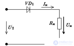
Solution:
Uload,avg =√2•U2/π = 30 V
U2 = 2.22 Uload,avg = 66 V
Urev,max = √2•U2 = 94 V
N= U1/ U2 = 220/66 = 3.33
9. Determine the capacitance of the filter capacitor Cfilter in a bridge rectifier, if the rectified voltage Uload,avg = 12 V, the current Iload,avg = 10 mA, and the ripple factor must not exceed 0.05.
Solution:
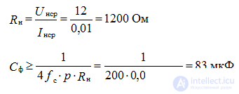
10. In a half-wave rectifier operating with Rload = 250 Ohm, the RMS value of the voltage on the secondary winding of the transformer is
U2 = 10 V.
Draw the circuit diagram of the half-wave rectifier.
Determine what permissible forward current the semiconductor diode should be chosen for,
Draw the time diagrams of the rectifier's input and output voltages.
Solution:
Uload,avg =√2•U2 / π = 4.5 V
Iload,avg = Uload,avg/ Rload = 4.5 / 250 = 0.018 A
Iforward = Iload,avg = 0.018 A
Iforward,perm = 1.3• Iforward = 0.0234 A
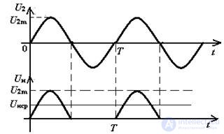
Time diagram of the rectifier.
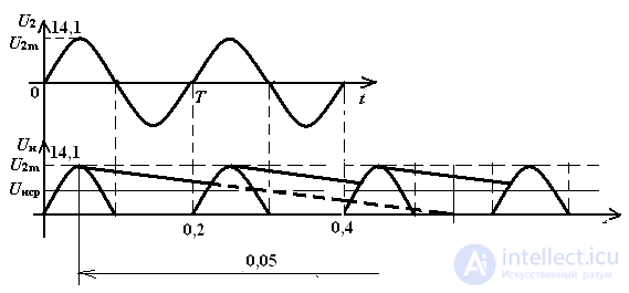
11. In a half-wave rectifier with a capacitive filter (fig.), the voltage on the secondary winding of the transformer is U2 = 10 V. The mains frequency is 50 Hz, Rload = 1 kOhm, Cfilter = 80 µF.
Determine the average value of the rectified voltage Uload,avg, Iload,avg, Urev,max, the ripple factor p, and plot the time diagrams.
Solution:
Uload,avg =√2•U2 / (1 + p) = 14.1/(1 + 0.2) = 11.75 V
Urev,max = 2√2•U2 = 28.2 V
τdischarge = C•Rload = 0.05 s
We plot the time diagrams:
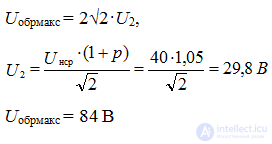
12. In a half-wave rectifier with a capacitive filter, the voltage across the load is Uload,avg = 40 V, and the ripple factor must not exceed 0.05.
What maximum reverse voltage Urev,max should the semiconductor diode be chosen for?
Solution:
VOLTAGE REGULATOR
1. What is the relative change in the output voltage of a parametric voltage regulator if the zener diode current changes by 2 mA, Ust = 8 V, Rdiff = 16 Ohm?
Solution:

2. A voltage u = Um(1.5 - 2t/T) V is applied to a chain consisting of a series-connected resistor R = 200 Ohm and a KS182 zener diode. Determine the current in the circuit at t = 0.2T, if the differential resistance of the zener diode is Rdiff = 30 Ohm, Um = 12 V.
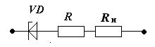
Solution:
i = (u – Ust) / (R + Rdiff)
U(0.2T) = 1.1Um
i(0.2T) = (14 - 8.2)/230 = 0.025 A
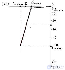
3. Draw the characteristic of a zener diode with the following parameters:
Ust = 12 V, Ist min = 3 mA, Rdiff = 25 Ohm
Ist max = 50 mA.
Solution:
∆Ist = Ist max - Ist min = 50 – 3 = 47 mA
∆ Ust = ∆Ist •Rdiff = 0.047•25 = 1.175 V
Ust min = Ust - ∆ Ust/2 = 11.42 V
Ust max = Ust + ∆ Ust/2 = 12.59 V
We plot the I-V characteristic of the zener diode as shown in the figure.
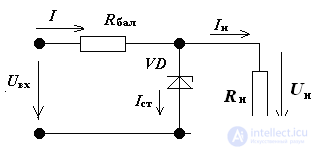
4. For the voltage regulator circuit, the zener diode has the parameters:
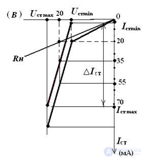
Ust = 20 V, Ist min = 1 mA, Rdiff = 40 Ohm, Ist max = 71 mA. Determine the current I in the circuit graphically, if Iload =20 mA:
Solution:
I = Ist + Iload
∆Ist = Ist max - Ist min = 71 - 1 = 70 mA
∆ Ust = ∆Ist •Rdiff = 0.07•40 = 2.8 V
Ust min = Ust - ∆Ust/2 = 18.6 V
Ust max = Ust + ∆Ust/2 = 21.4 V
We plot the I-V characteristic of the zener diode and the I-V characteristic of the resistor. We sum the characteristics. We graphically determine the current in the undivided branch of the circuit.
I = 55 mA
5. To stabilize the voltage across the load Rload = 2 kOhm, a parametric voltage regulator is used. The zener diode has the parameters:
Ist min = 1 mA, Ist max = 23 mA, Rdiff = 30 Ohm; the nominal output voltage is 11 V, the input voltage is 22 V.
Determine Kst and Rballast.
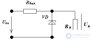
Solution:
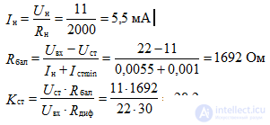
6. Determine the input voltage of the regulator. Parameters
of the zener diode: Ust = 12 V, Ist min =5 mA, Ist max=35 mA, Rdiff = 20 Ohm
Rballast = 800 Ohm, Rload = ∞.
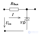
Solution:
current through the regulator
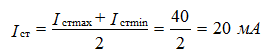
Since the zener diode and the ballast resistance are connected in series in the circuit,

By Kirchhoff's second law:

7. Determine U2 in the voltage regulator, if U1 = 16 V, R1 = 300 Ohm,
R2 = 1.2 kOhm, Ust min = 12 V, Rst = 15 Ohm.
Note: solve the problem analytically, using the equivalent circuit of the zener diode (an EMF source E = Ust connected in series with resistor Rst).
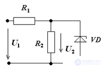
Solution:
Let us draw the equivalent circuit of the regulator
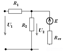
We use the two-node method:
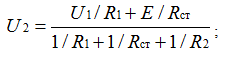
U2 = 12.2 V
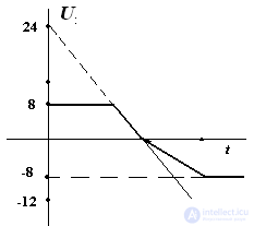
8. A periodic voltage u varies according to the law u(t) = 24(1 – 2t/T), where T is the period. The stabilization voltage of the zener diode is 8 V. R1 = R2 = 1 kOhm.
Plot the graph of the output voltage variation.
Assume the diode and the zener diode are ideal.
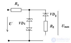
Solution:
During the positive half-period, diode VD2 is closed. The voltage Uout at t = 0 will equal the stabilization voltage. Starting from the moment
t = T/3 to T/2 it changes from 8 V to zero.
During the negative half-period, diode VD2 is open. With the zener diode branch disconnected, the voltage across resistor R2 changes from zero (at t = T/2) to – 12 V, at t = T. Connecting the zener diode branch limits the output voltage to – 8 V.
Transistors, amplifiers
1. Determine the base current and the current transfer ratio h21e of a BJT connected in a common-emitter configuration, if the increment of the collector current equals 17 mA and that of the emitter current is 18 mA. Determine the transistor currents IB, IC, IE and the voltages at its terminals relative to the common bus UB, UC, UE for the circuit.
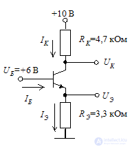
2. Determine the DC current gain of the transistor for the
circuit.
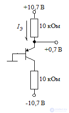
3. Determine the DC current gain of the transistor for the
circuit.
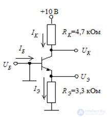
4. Determine the current IE in the bipolar transistor circuit.
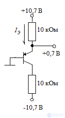
5. Determine the current IE and the voltage UC for the circuit.
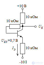
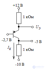
6. Determine the current IE and the voltage UC for the circuit.
7. Determine the output power of the voltage amplifier, if Rload = 40 Ohm, the voltage gain is 200, the input voltage is 0.01 V.
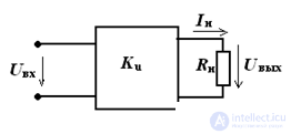
8. Determine the input voltage of the amplifier, if the resistance
Rload = 100 Ohm, Pout = 2.5 W, KU = 50.
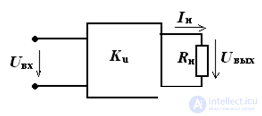
9. Determine the input voltage of the amplifier, if the resistance
Rload = 100 Ohm, Pout = 2.5 W, KU = 50.
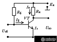
10. Determine the base current Ib and the voltage drop across the transistor Uce in the voltage amplifier, if Rb = 150 kOhm, Rc = 1.25 kOhm, Ec = 9 V, h21 = 40, Ube = 0
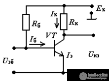
11. Determine the current gain KI and voltage gain KU of a two-stage amplifier, if the load resistance is 10 Ohm, the input voltage of the amplifier is 0.1 V, the power delivered to the load is 0.45 W, and the input resistance of the first stage is 100 Ohm.
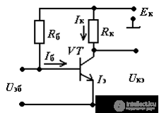
12. Determine the resistance Rc of the voltage amplifier, if Ec = 10 V, Ucep=4 V, Icp = 5 mA
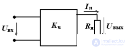
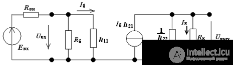
13. Find the values of Kgain, Rout in the voltage amplifier, if h11 = 900 Ohm, h21 = 50, h22 = 0.00016 S, Rc = 3 kOhm. Use the amplifier's equivalent circuit in the calculation.
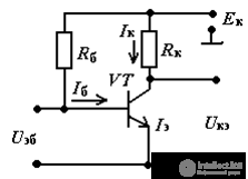
14. What is Ec equal to in the voltage amplifier, if Ucep = 7.5 V, Icp = 1 mA, Rout=2.5 kOhm?
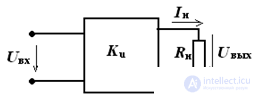
15. In a BJT voltage amplifier with a load Rload =250 Ohm, Uin = 0.1 V, Iload = 20 mA, Rb = 50 kOhm and transistor parameters h11 = 400, h21 = 40, h22 = 0, determine the voltage gain Ku and the output voltage. Use the amplifier's equivalent circuit in the calculation.
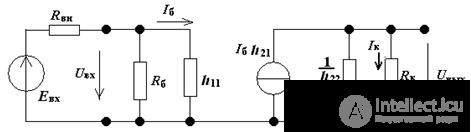
16. The parameters of the transistor connected in a common-emitter configuration in a single-stage amplifier are as follows: h11 = 250 Ohm, h22 = 0.63•10‾³, h21 = 50, the internal resistance of the signal source being amplified Rint = 250 Ohm, Ein = 10 mV, collector circuit resistance Rc = 2 kOhm, Rload = 200 Ohm.
Find the current gain, the voltage gain, the power gain, Rout, Rin of the amplifier. Use the amplifier's equivalent circuit in the calculation.
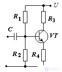
17. In the quiescent state, the collector current IKP = 2 mA, and the voltage on the collector equals half the supply voltage. The values of the resistors in the collector circuit are R3 = 5 kOhm and in the emitter circuit R4 = 1 kOhm. Determine the base voltage in the quiescent state and the resistances of the base divider resistors. Take the parameter h21 equal to 40.
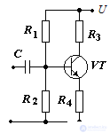
18. In the quiescent state, the collector current IKP = 100 µA, and the base voltage Ubp = 2 V. Determine the values of the resistors in the collector and emitter circuits at which the voltage gain equals 5. Parameter h21 = 40.
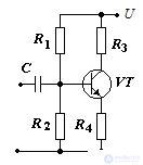
19. Determine the values of R1, R2, R3, R4 in a common-emitter amplifier stage, if the supply voltage U = 5 V and the gain of the stage equals 10. In the calculation take Ucp=0.4•E V, h21> 30, Icp = 200 µA.
20. Determine the voltage on the collector of the transistor for a common-emitter amplifier stage, if the supply voltage E=10 V, h21 = 50, R1 = 50 kOhm, R2 = 5 kOhm, R3 = 3 kOhm, R4 = 0.5 kOhm
Operational amplifiers
1. Determine the output voltage of the summing amplifier (fig.): if
U1 = U2 = U3 = 1V, R1 = 1 kOhm, R2 = 2 kOhm, R3 = 4 kOhm, R4 = 12 kOhm
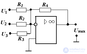
Fig.
Solution:
Uout = - (Kfb1U1+ Kfb2U2+ Kfb3U3) Kfb = - R4/ Ri
Uout = - (12U1+ 6U2+3U3) = - 1•21= - 21 V
2. What is the output voltage of the inverting amplifier, Fig. 3, if
R1 = 500 Ohm, R2 = 5000 Ohm, Uin = 0.2 V
Solution:
Kfb = - R2/ R1 = 10
Uout = Uin• Kfb = 2 V
3. A non-inverting amplifier based on an op-amp operates from a source with a voltage Uin =150 mV.
The resistances of the resistors are R1=20 kOhm, R2=200 kOhm.
Determine the amplifier's output voltage Uout and the gain KU.
Solution:
KU = 1 + R2/ R1 = 11
Uout = Uin• Kfb = 1.650 V
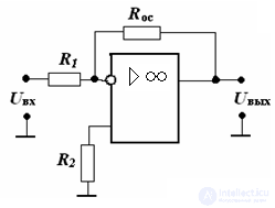
4. Calculation of an inverting amplifier.
Given: Uin = 80 mV, Uout = 4 V, Rload = 10 kOhm, op-amp type 14OUD7
MB=√2 – the frequency distortion factor in the upper frequency range. Calculate the values of R1, Rfb, R2 in the inverting amplifier.
Solution:
Determination of the resistor values.
Let us draw the amplifier circuit
Let us determine the amplifier's gain
Kfb = (Uout/Uin) = 4•103/80 = 50
We find Rfb from the relation
Rfb>=10•Rload = 10•10 = 100 kOhm
We determine R1:
R1= Rfb/ Kfb = 100/50 = 2 kOhm
Let us calculate the value of R2. This resistor is installed in the amplifier to balance the input currents.
R2= R1Rfb / ( R1+ Rfb) = (2•100/102) ~ 2 kOhm
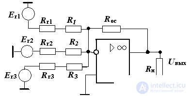
5. Calculation of a summing amplifier based on an op-amp.
Given:
Eg1 = - 2 V, Eg2 =3 V, Eg3 = 1 V, Rg1 = 0.5 kOhm, Rg2 = 0, Rg3 = 1 kOhm.
Gains for the inputs:
Kfb1 = 5, Kfb2 = 2, Kfb3 = 10, Rload = 2 kOhm. Op-amp type 153UD1.
Calculate the resistance values in the summing amplifier and determine Uout
Solution:
We choose Rfb >= 10•Rload, Rfb = 10•2 = 20 kOhm
From the expressions for the gains in the summing amplifier:
Kfb1 = Rfb/(R1 + Rg1) = 5
Kfb2 = Rfb/(R2 + Rg2) = 2
Kfb3 = Rfb/(R3 + Rg3) = 10
We find
R1 = 3.5 kOhm, R2 =10 kOhm, R3 =1 kOhm
We determine Rload, needed to balance the input currents
Rload = Rfb/(R1 + Rg1)/R2/(R3 + Rg3) = 1.3 kOhm
We find the output voltage of the summing amplifier:
Uout = Eg1• Kfb1 + Eg2•Kfb2 + Eg3• Kfb3 = 10 – 6 – 10 = - 6 V
We determine the output circuit current:
Iout = Ifb + Iload = Uout/Rfb + Uout/Rload = 3.3 mA
This value of Iout does not exceed the output current of the 153UD1 op-amp, which is 20 mA.
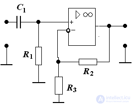
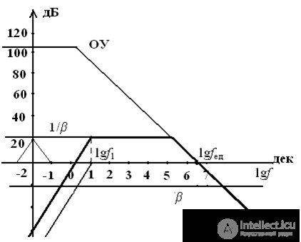
6. Plot the amplifier's log-frequency response (Bode plot), determine the gain, fl and fh, if
R1 = 20 kOhm, R2 = 10 kOhm, R3 = 100 kOhm K = 200000, funity = 3 MHz C1=0.7 µF
Solution: operational amplifier
Kdb = 20 lgK = 20•5.3 = 106 dB
lgfunity = 6.5 dec
Input circuit:
τ1 = R1• C1 = 20000•0.7•10-6 = 0.014 s
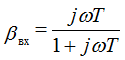
Break frequency of the input circuit's Bode plot:
f1 = 1/2πT1 = 11.4 Hz lgf1 = lg11.4 = 1.06 dec
Feedback element:
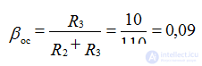
20lg βfb = 20 lg0.09 = - 20.8 dB
Since the amplifier uses "deep" negative feedback, Kfb = 1/β = 11
Constructing the Bode plot:
Часть 1 Electronics
Часть 2 - Electronics
Часть 3 - Electronics

Comments