
Lecture
Это продолжение увлекательной статьи про электроника .
...
Ec -Rc Ic
Using this equation we plot a straight load line - the "load line" - (the I-V characteristic of resistor Rc)
The line is plotted from two points:
Open-circuit mode: Ic =0 ; Uce = Ec
Short-circuit mode: Uce = 0 ; Ec = Rc Ic
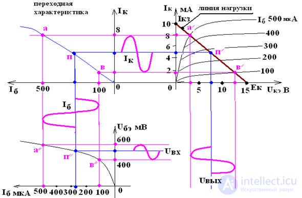
The intersection of the load line with the output characteristics determines the collector current Ic and the collector-emitter voltage Uce, for any base current Ib .
Rc is chosen based on the required amplification of the input signal, i.e. Rc is used to set the gain of the amplifier, while keeping the limits in mind: Uce max , Ic max , Pc max
Rc is usually 2-5 kOhm for low-power transistors
Determine the transistor's operating point:
Uceq ≈ Ec /2 Icq ≈ Ec /2Rc
Ibq ≈ Icq / h21
Ubeq ≈ 0.3 V for Ge
Ubeq ≈ 0.65 V for Si
The quiescent mode is provided by the resistance of resistor Rb: according to Kirchhoff's second law for the input circuit Ube = Ec - Rb Ib
Rb =(Ec - Ubeq)/ Ibq ≈ Ec / Ibq,
since Ec >> Ubeq
On the transfer characteristic, the linear section ab is selected; on it the signal is transferred from the input circuit to the output circuit without distortion.
2. Operating mode
Uin ≠ 0
Uin = Rin iin iin ≈ Ib => Ube = Ubeq + uin this causes ripples in the base current and the collector current:
Ib = Ibq + ib and Ic = Icq + ic
Output voltage ripples
Uce = Uceq + uce Uout = - Rc• ic
Capacitor C2 blocks the DC component of the collector voltage and passes only the AC component uce to the load device, which is the output voltage of the amplifier.
If uin, ic, ib stay within the linear sections of the input and transfer characteristics, then the shape of the output signal will be free of distortion and will match the shape of the input signal.
Amplifier characteristics
Amplitude characteristic (AC) of the amplifier
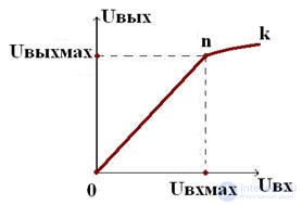
The straight line - section 0n, the linear part of the AC, can be determined by
Kamp = Uout /Uin
Along the section hk the amplitude characteristic is nonlinear, and the gain Kamp decreases.
Amplitude-Frequency Characteristic
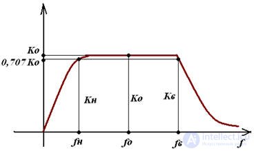
The range of frequencies over which the gain does not depend on frequency is called the amplifier's passband and is denoted Δf.
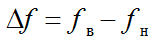
where fL - lower frequency,
fH - upper frequency
Frequency properties of an amplifier
At ω < ωL, the reactance of the coupling capacitors has a strong influence
XC1.2 = 1/ ωL C1,2 , it becomes large and its influence is significant (C1,2~ 1μF).
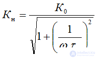
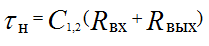
At ω>ωH the influence of C12 is small, but the element C0 begins to have an effect, shunting Rload, and KU decreases.
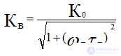
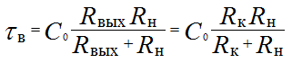
The decrease in gain is estimated by the frequency distortion coefficient:
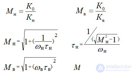
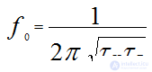
Quasi-resonant frequency at which Ko is maximal
Amplifier stage with temperature stabilization
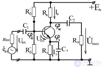
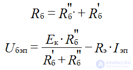
According to Kirchhoff's second law

Calculation of the amplifier's element parameters
Rb =(Ec - Ubeq)/ Ibq ≈ Ec / Ibq
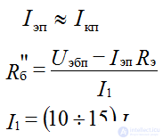
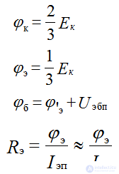
Emitter follower (current amplifier)
An amplifier in which the transistor is connected in the common-collector configuration is called a current amplifier.
The main resistor from which the output voltage is taken is included in the emitter circuit. The collector is connected to the common point (ground) of the amplifier, since the internal resistance Rin of the supply source Ec is small.
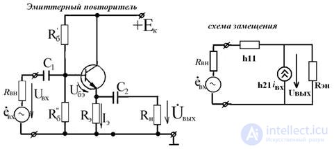
Main parameters:

Gain
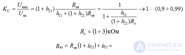
Output resistance

Current gain
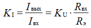
Comparing the current amplifier with the voltage amplifier, we can draw the following conclusions:
the input and output voltages are in phase;
the input resistance is (1 + h21) times greater than in a voltage amplifier;
the output resistance is (1 + h21) times smaller than in a voltage amplifier
Field-effect transistor amplifier
Amplifiers based on field-effect transistors are widely used because they have a higher input resistance than amplifiers based on bipolar transistors, a lower output resistance, better temperature stabilization, and better radiation resistance.
The design of field-effect transistor amplifiers is the same as that of BJT amplifiers.
Common-source field-effect transistor amplifier
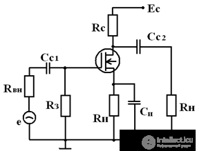
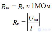
Rg is a resistor that provides a potential at the gate that is negative with respect to the source. Rg=(0.1-0.03)Rgs for DC
Amplifier parameters
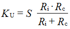
Ri - the internal resistance of the field-effect transistor.
Multistage amplifiers
Amplifiers consisting of several stages, intended to increase the gain, are called multistage amplifiers.
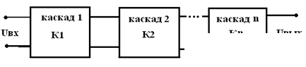
The coupling between the amplifying stages of a multistage amplifier is achieved in various ways:
• the input of the next amplifying stage is connected to the output of the previous one by means of resistors - direct (galvanic) coupling;
• the input of the next amplifying stage is connected to the output of the previous one through a coupling capacitor Cc and a resistor Rc connected in parallel with the input of the next amplifying stage - resistive-capacitive coupling.
Two-stage amplifier
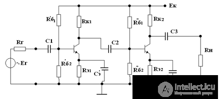
The voltage gain for mid-frequencies K = K1*K2*…Kn.
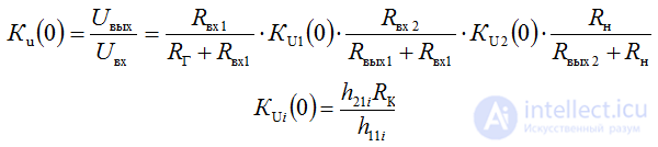
Voltage dividers reduce the overall gain by several times, typically by 3-5. This must be taken into account when designing the amplifier.
• As the number of stages increases, the frequency distortion coefficient is determined by the formula:
M = M1•M2…,
if the number of stages is n, then M increases n-fold.
• Phase of the output signal: φ = φ1 + φ2 +…
• the gain increases, but the passband narrows.
For a two-stage amplifier: the frequency distortion coefficient increases 2-fold, and the phase of the output signal is equal to the phase of the input signal
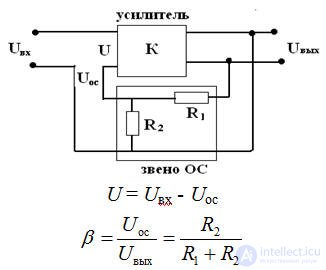
Effect of negative feedback on the parameters and characteristics of an amplifier
Gain
Negative feedback reduces the gain of the amplifier by a factor of (1+βK).

If βK>>1, then the gain, taking feedback into account, does not depend on the parameters of the amplifier itself; such feedback is called "deep" feedback

the input resistance increases by a factor of (1+βK)
the output resistance decreases by a factor of (1+βK)
the passband widens -
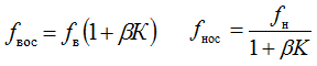
Negative feedback increases the stability of the gain, and improves the amplifier's properties; the level of nonlinear distortion is reduced.
Properties of positive feedback (PFB)
• U = Uin + Ufb; Kfb = K / (1- βK);
• the gain increases when positive feedback is introduced;
• the input resistance decreases;
• the output resistance increases;
• the passband narrows;
• the amplifier's stability worsens;
• the level of nonlinear distortion increases..
Amplitude-frequency characteristic taking feedback into account
Amplitude characteristic taking feedback into account
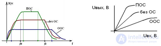
Power amplifiers
Power amplifiers form an independent group of electronic devices with special properties: they can amplify both current and voltage to obtain the required power at the load, and they also have an output resistance matched to the resistance of the electrical energy receiver.
The output resistance of an amplifying stage in which the transistor is connected in the common-emitter (or common-source) configuration is hundreds of Ohms or units of kOhms, whereas the resistance of a load device that consumes significant power is units to tens of Ohms. With such a ratio of resistances, the power dissipated in the load device is given by the formula 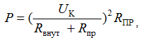 , which follows from the analysis of the equivalent circuit, Figure 4.
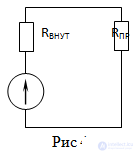
The load devices of power amplifiers are:
• motor windings
• relays
• loudspeakers and other elements of electrical circuits with small resistances (from 1 to 10 Ohms)
These devices require significant amplified-signal power (from 10 to 100 W)
• The main figure of merit is the power gain Kp = Ku•KI
• Obtaining the required power in the load device is ensured by selecting the appropriate transistor and by the equality Rout amp = Rload
For matching, the following are used:
• a step-down transformer
• an emitter follower
Transformerless power amplifier
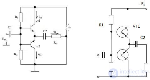
Fig 5 Push-pull power amplifier
The push-pull power amplifier of Fig. 5 is built using transistors of different conductivity types:
T1 - of the n-p-n type; T2 - of the p-n-p type
T1 and T2 are connected in the common-collector configuration; it is necessary that the transistors of different types have strictly identical parameters. If discrete components are used, complementary pairs of transistors are chosen
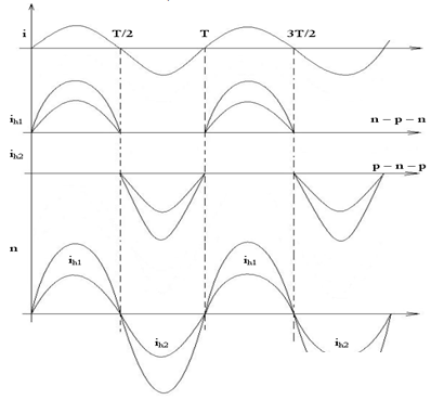
Direct current amplifiers
In measurements, electronic devices need to amplify signals of very low frequencies (fractions of a Hz). Direct current amplifiers are designed to amplify signals that change slowly over time, i.e. signals with f→0.
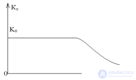
Fig. 1 amplitude-frequency characteristic of a direct current amplifier
Uout is determined by the amplified useful signal and a spurious signal produced by changes over time in the DC operating parameters of the stages.
Zero drift
The spontaneous change in Uout of a direct current amplifier with a constant input Uin = const is called zero drift.
• Udr =DUoutdr/KU;
• KU - the gain of the amplifier,
• Udr - the spurious input signal.
DC amplifier circuit
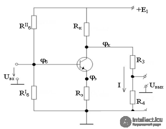
Fig. 2 Direct current amplifier
The direct current amplifier in Fig. 2 has two power supplies, +E1 and -E2, which create positive and negative voltages relative to the common point (which has zero potential).
Across the divider R3 - R4 is applied UR3 + UR4 = jc + E2, and the potential of the divider's midpoint must equal zero, so that Uout=0; hence UR3 = jc, UR4 = E2.
Uin >> Udr for normal operation.
So as not to disturb the transistor's operating mode, a current I = (0.02-0.1)Ic must flow through the divider; I ≤ Ic.
R3 = UR3/I; R4 = UR4/I
The divider at the output of the direct current amplifier compensates for the DC component of the collector voltage, but transfers the amplified voltage from the transistor's collector to the amplifier's output with some attenuation.
K = Ko•R4/(R3 + R4);
Ko - the gain without the divider. In practice Ko is reduced by a factor of 1.5-2.
To combat zero drift the following are used:
• stabilization of the supply voltages;
• stabilization of the temperature regime;
• differential direct current amplifiers.
Differential amplifiers
These are designed to amplify the difference of potentials (voltage, current) applied to two inputs. The simplest circuit of this type of amplifier is shown in Fig. 3.
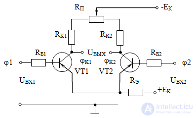
Fig. 3 Circuit of a symmetrical differential amplifier using two bipolar transistors
The symmetrical differential amplifier, whose circuit is shown in Fig. 3, consists of two identical, single-stage DC amplifiers connected in parallel with respect to the power supply. Input voltages (potentials), relative to the common terminal (the joined emitters), are applied to the corresponding base terminals, and the output voltage, as the potential difference relative to the same common terminal, is taken from the transistors' collector terminals.
If  . The same result occurs if the voltages at both inputs are equal in absolute value and have the same sign, i.e. when

If the input voltages do not match in sign or in absolute value, then a voltage appears at the output equal to the difference of the amplified voltages at the collectors of VT1 and VT2. Thus

where K is the gain of one arm; the terms in parentheses represent the algebraic sum of the input voltages taking the sign of the potential into account: for a negative potential at the input, the sign of the input voltage is reversed.
It should be kept in mind that such an amplifier has no common point between the signal source and the load: the output voltage is taken from the load resistance, which is connected to both collectors, and is measured as the potential difference between them.
The resistance RE has a relatively large value, which creates a current-source mode in the emitter circuit of both transistors. In this case, by Kirchhoff's first law, there is no increment of current in the emitter circuit when the currents in the arms of the differential amplifier change. The emitter circuit serves to stabilize the quiescent mode and, in the differential stage, does not affect the gain: thus there is no AC feedback.
Since the differential stage amplifies a difference of potentials, when common-mode voltages (voltages of the same polarity, phase, and amplitude) are applied to its inputs, the output voltage will be zero. For example, the electromagnetic field of the mains voltage may induce an EMF of the same sign and magnitude at the inputs of the differential amplifier, which will not be transferred to the output owing to mutual cancellation at the output. In a single-stage voltage amplifier this effect is absent, since the voltage at the collector terminal of the single transistor is measured relative to the same common point as at the input.
The quality of common-mode rejection is characterized by the common-mode rejection ratio, whose unit is decibels (dB). 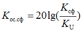
With a high degree of stage symmetry, the common-mode rejection ratio is

Single-ended differential amplifier
A simpler variant of the single-ended differential amplifier circuit is shown in Fig. 4.
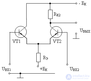
Fig. 4 Circuit of a single-ended differential amplifier
Here, the left arm on VT1 is essentially a common-collector amplifier. The resistor RE plays the same role as in the symmetrical differential amplifier. However, in the single-ended amplifier it is possible to take the output voltage relative to the common point, which allows this type of differential amplifier to be matched with single-ended voltage or power amplifiers.
Obtaining an output voltage of either polarity is achieved by using a bipolar power supply -E and +E. According to Kirchhoff's second law, when moving from +E to -E through VT2, the potential passes through zero. Thus, in the quiescent state, a mode is possible in which UOUT = 0 when there are no voltages at the inputs.
When a negative-polarity voltage Uin1 is applied to the input of VT1, its collector current increases, and consequently the collector current through VT2 decreases (the current through Re remains constant), for Uin2. This leads to an increase in the positive potential at the output, since the voltage drop across Rc2 decreases.
When UIN1 = 0 and there is a negative potential at the input of VT2, it opens and the current through it increases, which leads to an increase in the voltage drop across Rc2 and, accordingly, the potential at the output decreases. That is, the output voltage changes polarity. With potentials of equal magnitude and sign at the inputs, the output voltage will be zero, since the collector currents of transistors VT1 and VT2 do not change.
One of the inputs of the single-ended differential amplifier has a potential sign that matches the output and is therefore called the non-inverting input. The input of the differential amplifier whose potential sign is opposite to the sign of the output potential is called the inverting input.
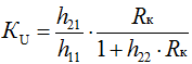
Main parameters
1. Uout = U21 = Ku*(Uin1 - Uin2)
2. Rin da = 2h11
3. Rout da = 2Rc/(1+h22Rc) » 2Rc
Differential amplifiers (DA) are used: in op-amps as the main input stage, in stabilizers; and as separate integrated circuits. Series K118 UD1, K122 UD1, K175 UV, and others
Operational amplifiers
An operational amplifier (hereafter op-amp, or amplifier) is an analog electronic microdevice with a differential input, intended for amplifying and generating electrical signals, performing mathematical operations in analog form, creating electrical filters and threshold devices, i.e. for performing various operations on electrical signals.
Internal structure of the operational amplifier
The internal structure of the operational amplifier is shown in Fig. 5. The input block is a differential amplifier (DA), which may consist of 3-4 stages. To create a large internal gain, a voltage amplifier (VA) block is used. A power amplifier (PA), built using a transformerless circuit, is normally used as the output block.
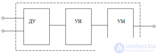
Fig 5. Block diagram of an operational amplifier
An op-amp has two inputs and one output. One of the op-amp's inputs is called the inverting input, since when a voltage is applied to it, its sign at the output becomes opposite. The other input is called the non-inverting input: when a voltage is applied to it, its sign at the output does not change. This behavior of the op-amp is possible because it is powered from two voltage sources of different signs. As a result, the output block of the op-amp, under certain conditions, has a virtual zero potential, relative to which the sign of the potential (the output voltage) can change in either direction relative to the common terminal. As in any amplifying device, an op-amp can be enclosed in a feedback (FB) loop
Parameters of the operational amplifier
Depending on the operating mode, an op-amp is characterized either by static or by dynamic parameters.
The main static parameters of an op-amp include:
1. The gain Ko. Its value can be 
2. The unity-gain bandwidth f1 - the upper frequency at which the gain drops to unity. The value of f1 for a number of op-amps reaches  Hz.
Hz.
3. The zero offset voltage UOS - the potential difference between the inverting and non-inverting inputs that must be applied so that the output voltage equals zero. This potential difference in operational amplifiers is 0.001-10 mV, depending on their quality.
4. Input bias currents 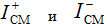 - the currents at the non-inverting input and the inverting input respectively when they are grounded. The magnitude of these currents is on the order of tenths to thousandths of a microampere. In modern op-amps this parameter can be
  A.
A.
5. The average input bias current  - half the sum of the input bias currents.
6. The input offset current  - the difference of the magnitudes of the input bias currents.
The main dynamic parameters of an op-amp include:
7. The slew rate of the output voltage  - the ratio of the change in the output voltage of the op-amp to the time interval over which this change is observed. The value of this parameter is 0.1-100 V/μs.
8. The common-mode rejection ratio Kcmr - the ratio of the change in common-mode input voltage to the input voltage that would cause the same change in output voltage. Modern op-amps have Kcmr=70-120 dB.
In operational amplifiers the input stage is implemented as a differential circuit with a single-ended output
Standard graphic symbols for op-amps
The standard graphic symbols (SGS) of the operational amplifier (op-amp) are shown in Fig. 6.
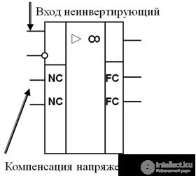
Fig. 6,a shows the full symbol
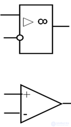
Fig. 6,b - the simplified symbol of the op-amp.
Inputs are shown on the left, outputs on the right. Terminals intended for connecting the power supply (+U, -U), offset-voltage compensation circuits (NC), and frequency-correction circuits (FC) are shown in additional field zones on either side of the symbol.
For convenience in analyzing how an op-amp operates in various circuits, the concept of an ideal op-amp is used. An ideal op-amp is one in which the differential voltage at the inputs  is always automatically maintained at zero by the op-amp itself when there is a feedback path to the inverting input (this holds when Uos=0), the input current
  , the unity-gain bandwidth
  , and the output resistance equals zero, Rout = 0.
From these properties of an ideal op-amp's parameters it follows that the potentials of the inverting  and non-inverting
  inputs are equal:
  , and the current through the input elements equals the current in the feedback loop.
Uout = (Uin1-Uin2)∙Koa the difference voltage is called the differential input signal. This is the voltage applied between the inverting and non-inverting inputs.
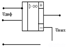
Fig. 7 Circuit for determining the differential voltage.
• If both inputs of the op-amp are connected together, the resulting circuit, Fig. 8, will have only one input, and the voltage applied to it is called the common-mode voltage Ucm = Uin1= Uin2.
• For the common-mode circuit, the output voltage must equal zero
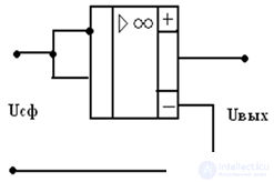
Fig. 8 Circuit for determining the common-mode voltage
Characteristics of an Operational Amplifier
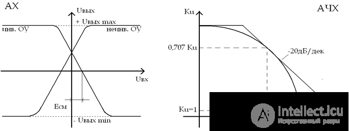
Op-amp parameters
Static:
– Gain
– Input resistance
– Output resistance
– Offset voltage
Common-mode rejection ratio
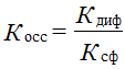
Dynamic:
1. Cutoff frequency fcut – the value of this frequency corresponds to a decrease in the magnitude of the op-amp's gain by a factor of √2 (3 dB)
fcut is the op-amp's bandwidth.
2. Unity-gain frequency f1 – at which Kou decreases to 1. For modern op-amps
f1 = 10,000–10,000,000 Hz.
3. Maximum output voltage slew rate Uout ~ 0.1–100 V/µs.
4. Settling time tset.
Basic parameters of an ideal operational amplifier
• Differential gain Kdiff →∞
• Common-mode gain Kcm = 0
• Input resistance Rin →∞
(input currents equal 0)
• Output resistance Rout = 0
Classification of op-amps
• general-purpose (K140UD7) K=1000…100000, Eoff=4mV, f1=0.8MHz
• precision or instrumentation (K140UD24) K=1000000, Eoff=5µV, f1=2MHz
• high-speed (154UD2) K=10000, Eoff=2mV, f1=50MHz
• micropower (K1423UD1) K=10000, Eoff=5mV, f1=1.5MHz
Circuit design of electronic devices based on operational amplifiers
Operational amplifiers with deep negative feedback
Operational amplifiers with deep negative feedback are used to build various computing amplifiers.
Basic connection schemes for operational amplifiers
• Non-inverting amplifier;
• Inverting amplifier;
• Differential-input amplifier 1
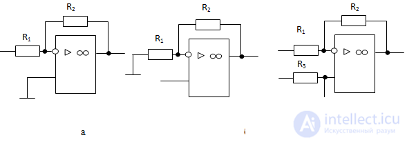
Fig. 1. Op-amp connection schemes: inverting (a); non-inverting (b); differential (c).
Non-inverting amplifier
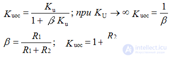
Inverting amplifier
Kuoc = - R2/R1
In differential connection of the op-amp, input voltages are applied to both inputs through resistors R1 and R3. In this case, the equality of potentials at the inputs is maintained.

It follows that

When R1=R3; R2=R4, it follows that:
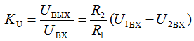
where the value in parentheses is the voltage difference taking sign into account
Summing amplifier.
Fig. 2 shows an amplifier circuit based on an op-amp that performs the function of a summing amplifier.
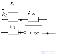
Fig. 2. Summing amplifier based on an op-amp with frequency-independent elements.
Based on Kirchhoff's 1st law for node 1
 or
or 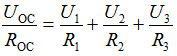
That is, the output voltage of the amplifier circuit equals the input voltages with weighting coefficients equal to the gain for the corresponding input:
Differentiator.
The use of reactive elements makes it possible to implement analog differentiation and integration operations. If in the circuit the input element is a capacitor with capacitance C, and the feedback element is a resistor with resistance R, then from the condition I1=I2 it follows that
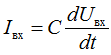 hence
hence 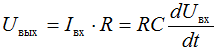
i.e., the output voltage is the derivative of the input voltage with weighting coefficient RC.
Integrator.
In the case where a resistor is connected to the inverting input, and a capacitor is placed in the negative feedback loop, the operational amplifier circuit performs the function of an integrator:

i.e., the output voltage is the integral of the input voltage.
Example.
If the voltage on the input resistor changes as a step from 0 to U0, then the op-amp's output voltage will change according to the law 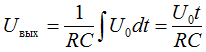 , i.e., it will grow proportionally to time. This corresponds to the case of charging a capacitor C with a constant current Iin=Uin/R
Electrical signal generators
An electronic oscillator is a device that converts the energy of a DC power source into electromagnetic oscillation energy of a given shape, required frequency, and power.
Electronic oscillators of harmonic (sinusoidal) oscillations and pulse (relaxation) oscillations are distinguished.
Classification of oscillators
Depending on frequency, oscillators are divided into three types:
1. low-frequency
2. high-frequency
3. ultra-high-frequency
Depending on the type of excitation, oscillators are divided into:
1. externally driven
2. self-excited (self-oscillators)
There are several oscillator operating modes:
1. self-oscillation
2. standby (gated)
3. synchronized
Block diagram of an oscillator
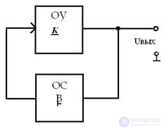
self-excitation conditions

• two conditions that must be satisfied simultaneously:
1. amplitude balance condition

2. phase balance condition (only at the resonant frequency)

• To obtain stationary steady oscillations in a self-oscillator, the following condition must be satisfied:

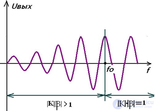
High-frequency oscillator
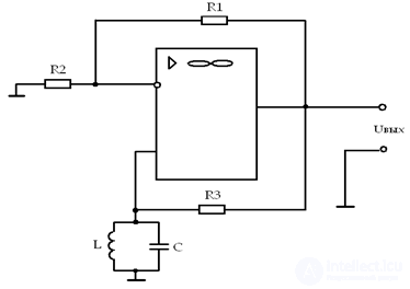
• the self-excitation condition is used – the amplitude and phase balance condition at the resonant frequency, R3>>Rfb
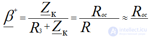
• For the oscillations to be slightly larger in amplitude, the condition  is required
Low-frequency oscillator
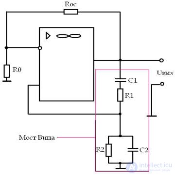
• An op-amp with a negative feedback element on Ro Rfb, setting the gain K=3.
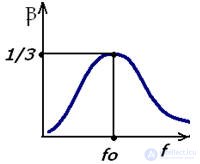
• Wien bridge – a positive feedback element on R1C1 and R2C2, having a transfer coefficient
β = 1/3 and ψ = 0, where R1=R2=R, C1=C2=C
• Self-oscillator frequency:
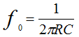
To adjust the frequency, either R1 and R2 are changed (fine adjustment) or C1 and C2 via switches. The output will be a pure sine wave if a thermistor or an incandescent lamp is placed in the negative feedback loop (as current increases, resistance increases).
Parameters
• frequency f
Sinusoidal-oscillation generators hold frequency better than generators of other waveform shapes.
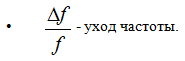
The task is to improve this parameter, i.e., to reduce it to zero
Applications of oscillators
• as a component part of measuring instruments and automatic systems
• for powering instruments that monitor the composition and quality of various substances
• for powering installations for high-frequency heating of metals, etc.
• Audio-frequency and high-frequency oscillators in radio engineering and electronics.
Pulse generators
Electronic switches
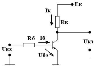
• Switch "open" – the transistor operates in cutoff mode, i.e., the minimum current flows through the transistor ic = 0, Uce = Ec. The transistor's resistance is very high – an open circuit.
• Switch "closed" – the transistor operates in saturation mode: Uce = 0, current limited by resistor Rc – the transistor enters saturation mode when the transistor's resistance in this mode equals zero.
• When a transistor switch toggles from the open state to the closed state and back, this occurs abruptly, and the power losses involved are negligible.
Pulsed operating mode of a device is a brief application of a signal alternating with a pause.
Pulse shapes:
• Rectangular
• Triangular
• Sawtooth
• Exponential, etc.
the most common pulse shape is rectangular.
Pulse parameters:
Pulse period Tp or frequency fp = 1/Tp
Pulse amplitude Up
Pulse duration tp
Rise time tr
Fall time tf
Pause duration tpause
Comparator
A comparator is a device designed to compare a measured input signal Uin with a reference voltage Uref.
Voltage comparators are ICs designed to compare two voltages and output the comparison result in logical form: high signal level, low signal level
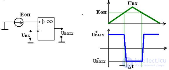
There are three types of comparators:
• High-speed Δt ≤ 1ns
• Medium 1ns ≤ Δt ≤ 10ns
• Slow Δt ≥ 10ns
SCHMITT TRIGGER
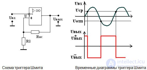
If positive feedback is introduced into a comparator, such a device is called a Schmitt trigger.
A trigger (flip-flop) is a device having two states of stable equilibrium and capable of switching abruptly from one state to another under the influence of an external control signal.
A state of stable equilibrium is characterized by the fact that after a weak disturbance the device returns to its initial state, i.e., the currents and voltages return to their original values.
Multivibrators
In a multivibrator operating in self-oscillation mode, rectangular pulses are continuously generated at its output.
Any multivibrator, as a pulse generator, consists of an amplifier and RC circuits.
Symmetric multivibrator
The pulse duration tp and the pause duration tpause are equal.
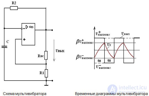
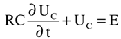
The capacitor charging process is described by the differential equation:

Solution of this equation:

If the capacitor charging process begins at time t2 and ends at time t3, then for this circuit the solution can be written as:
Let UC(tp) = β Uout max. Taking the logarithm of this expression, we get:
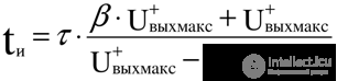
If U+out max = U-out max, then: tp = τ ∙ln(1+2 R1/ Rfb)
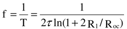
if tp = tpause, then the multivibrator is symmetric; in such an oscillator the oscillation frequency is determined by the formula, where the period T = tp + tpause
Asymmetric multivibrator
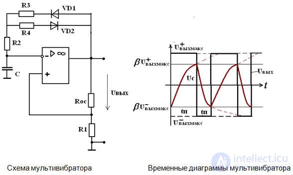
An asymmetric multivibrator is a rectangular pulse generator in which the pulse duration is not equal to the pause duration, i.e., tp≠ tpause.
tp =(R2+R3)•C• ln (1+2 R1/ Rfb)
tpause =(R2+R4)•C• ln (1+2 R1/ Rfb),
where R3 ≠ R4.
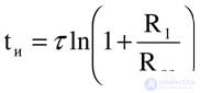
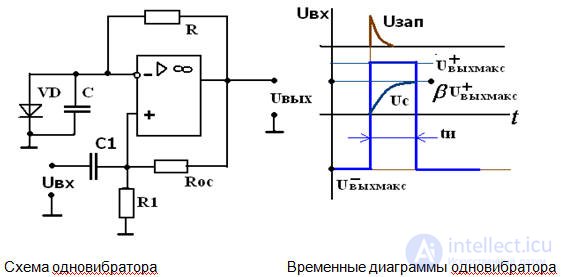
One-shot (monostable)
A multivibrator operating in standby (gated) mode, where a rectangular pulse appears at the output only when a trigger pulse is applied to the enable input.
Fundamentals of digital electronic engineering.
Logic and digital devices
Mathematical apparatus
• Number systems (decimal, binary, hexadecimal) – a way of representing a number with a set of digits;
• Boolean algebra;
• The unit of information in digital systems is the bit (BInary digiT).
A bit can take two values – zero and one.
• A group of eight bits makes up a byte.
1 byte = 8 bits – a binary word;
16 bits = 2 bytes – a machine word;
4 bits = ½ byte – a nibble.
Number systems
• The decimal number system uses digits from the natural number sequence.
• In digital electronic devices, the binary number system is used, in which only two values, 0 and 1, are used – machine language.
• The hexadecimal system is more compact.
Binary number system
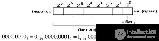
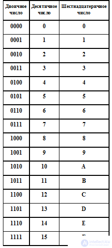
Converting a binary number to decimal form.
00010100=27•0 + 26•0 + 25•0 + 24•1 + 23•0 + 22•1 + 21•0 + 20•0=16 + 4=20
Converting from a decimal to a binary number is done by successive division by 2.
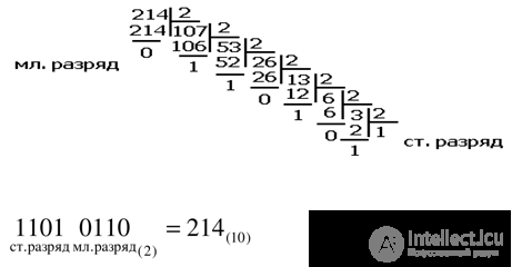
Binary number Decimal number Hexadecimal number
Boolean algebra
• Each specific set of variable values can be viewed as an n-bit binary code, so the number of such sets is .
• Any Boolean function of variables can be specified by a truth table, or analytically in the form of structural formulas.
Rules and relations in Boolean algebra:
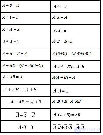
The commutative and associative laws of mathematics apply
A+B=B+A
AB=BA
A(B+C)=AB+AC
ABC+AC+AB+BC=AC(B+1)+B(A+C)
Logic elements
A binary logic element is an electronic circuit whose output state is described by one of the basic Boolean functions.

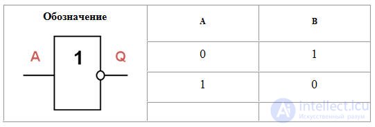
The "NOT" logic element
element symbol, truth table, and structural formula
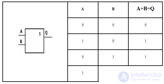
The "OR" logic element
element symbol, truth table, and structural formula
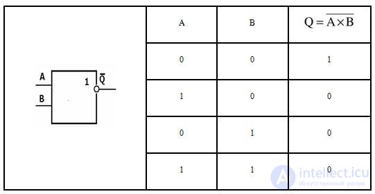
The "NOR" element (inverse disjunction)
element symbol, truth table, and structural formula
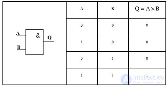
"AND" – logical multiplication (conjunction)
element symbol, truth table, and structural formula
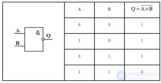
The "NAND" element (inverse conjunction)
element symbol, truth table, and structural formula
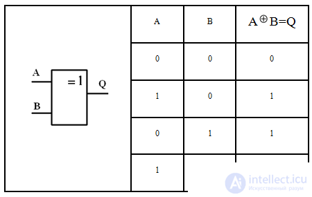
Exclusive OR
element symbol, truth table, and structural formula
Combined logic elements
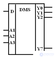
The "NOT," "AND," "OR," and other elements are combined to implement more complex logic functions: encoders, decoders, multiplexers, demultiplexers, half-adders, etc.
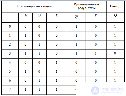
Analysis of logic circuits
Analysis of logic circuits is the process of constructing a truth table from a logic circuit.
The truth table of a complex element can be constructed from the truth tables of the individual simplest elements.
Example of analyzing a logic device

Let us construct the truth table
Synthesis of logic circuits
Synthesis of logic circuits is the construction of logic circuits from a given truth table.
Synthesis rules
1. Based on the output value Q, the number of "0"s and "1"s is determined; if "0"<"1", then synthesis is performed for the rows where Q=0 (if "1"<"0", then for the rows where Q=1)
2. Each row is implemented by a single "AND" element with corresponding "NOT" elements on the inputs.
3. An "OR" device, if synthesizing by "1," or "NOR," if synthesizing by "0," performs the conversion of the signals into the output value Q.
Minimization using Karnaugh maps or using the canonical disjunctive normal form (CDNF)
• A structural formula is constructed
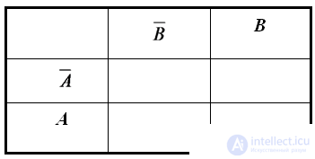
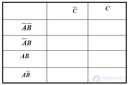
• A Karnaugh map is constructed for two, three, four, etc. variables
for two variables
for three variables
A set of Boolean algebra rules
De Morgan's theorems
The complement of a sum equals the product of the complements of the variables

The complement of a product equals the sum of the complements of the variables

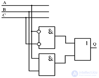
Example
Given: synthesize the function represented by the structural formula

Let us write the equation in canonical disjunctive normal form (CDNF)
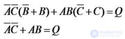
Final circuit
Flip-flops
Basic concepts
A flip-flop is an electronic device that can retain one of two possible states.
The inputs of a flip-flop are divided into:
setting inputs — for setting the flip-flop's initial state;
data inputs — for entering information;
clocking inputs — for setting the moment of triggering of the flip-flop.
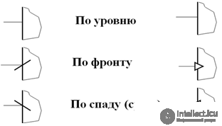
Flip-flops are triggered on the rising edge or the falling edge
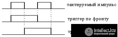
Symbols for the action of the clocking pulse
Asynchronous RS flip-flop
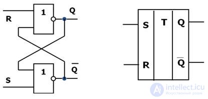
S - set – set to "1" Symbol
R – reset – reset to "0"
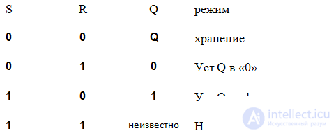
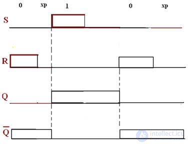
RS is an asynchronous flip-flop, i.e., the transition from one state to another is not tied to clock pulses.
Truth table of the RS flip-flop
Timing diagrams of the asynchronous RS flip-flop
Synchronous RS flip-flop
Symbol
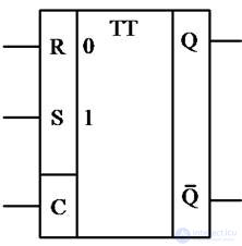
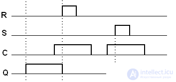
Initially with Q="1", a change to "0" is possible when R and C are "1"; if Q=1 is needed, then S=1 and C=1, and so on.
Timing diagrams
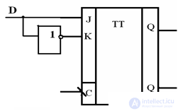
D flip-flop
The D flip-flop (data delay flip-flop) is a synchronous flip-flop whose output state matches the signal on its data input (D input) that it had during the previous clock pulse
Symbol and truth table for edge-triggered operation of the flip-flop
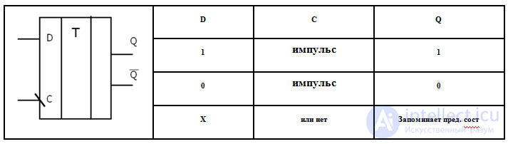
Timing diagrams
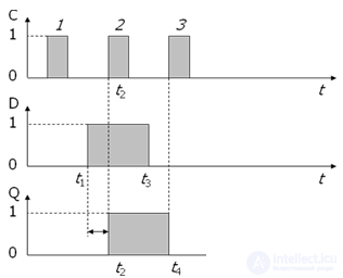
The D flip-flop delays the information present at input D by 1 clock cycle.
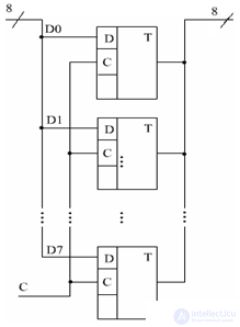
Registers can be built from D flip-flops; to fill an 8-bit word, 8 D flip-flops are needed.
Information in D flip-flops is stored until an enable signal for changing the information arrives, at which point a new number is written
T flip-flops
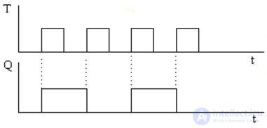
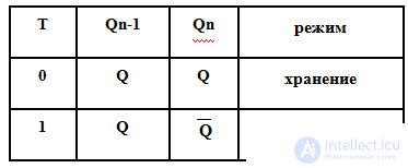
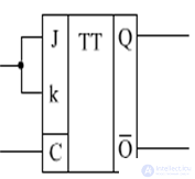
A counting flip-flop (T flip-flop) changes its state each time there is an active signal level on its single data input T.
Symbol
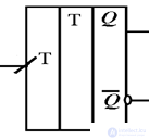
The T flip-flop is a divide-by-2 frequency divider.
Timing diagrams
Truth table
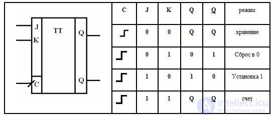
JK flip-flop (universal)
Symbol Truth table
Timing diagrams
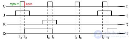
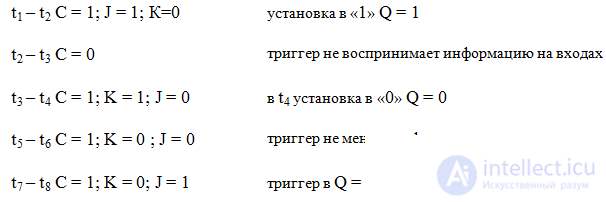
If J and K are connected together, we get a T flip-flop. T flip-flop, with C=1
D flip-flop built from a JK flip-flop
Digital counters
A pulse counter is a device designed to count the number of pulses applied to its input. The count result is stored in binary code
A digital circuit that performs the counting function can be assembled from flip-flops and logic elements.
Counters are built on the basis of JK or T flip-flops
The counter's bit width is determined by the maximum number up to which it counts in binary code
to build a modulo-16 counter, 4 flip-flops are needed
CT2 – a two-bit binary counter
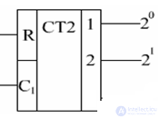
Outputs: 1, 2 – designation of binary digits
C1 – clock (counting) input
R - reset to 0
Counters are used:
• for counting numbers, pulses, time intervals,
• for ordering sequences,
• for addressing,
• for building frequency dividers,
• for building memory elements.
Modulo counters
The modulus of a counter shows the number of distinct states the counter passes through during one full counting cycle.
Example 1. For counting modulo 5, the cycle is the sequence of binary numbers: 000, 001, 010, 011, 100 (i.e., 0, 1, 2, 3, 4).
Example 2. At the output of a 4-bit binary counter, 4 binary digits are activated; such a counter counts from 0000 to 1111 (i.e., from 0 to 15).
Asynchronous decimal counter. (Modulo-ten counter)
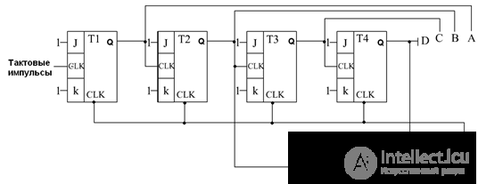
It counts from 0000 to 1001 (from 0 to 9), i.e., 4 binary digits are needed – 8 4 2 1 – therefore, the counter is implemented using four JK flip-flops and a NAND element. The flip-flops are in toggle mode J=K=1. The clock pulses trigger only the first flip-flop T1, flip-flop T1 triggers T2, and so on.
Such a flip-flop chain is called a ripple counter or a counter with a carry chain.
Each higher-order digit switches half as often as the previous one. The NAND logic element is used to reset all flip-flops to "0" upon the arrival of the tenth pulse (1010), i.e., when a logical "1" is applied to D and B at the NAND element, all flip-flops are reset to zero, and the counter starts counting pulses again; the NAND provides the reset.
Synchronous counters
To increase the speed of digital devices, counters must operate synchronously with the clock pulses. This task is implemented in synchronous counters.
Let us consider a 3-bit modulo-8 counter.
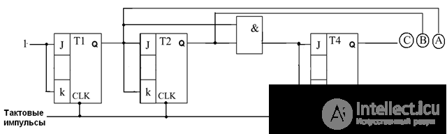
The JK flip-flops operate in toggle mode and in hold (blocking) mode
Registers
A register is a digital device designed for temporary storage of a numeric code and its conversion.
Symbol for a four-bit register
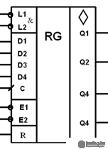
L1&L2 – write;
E1∨E2 – output disable;
The main elements of a register are binary cells, which are D flip-flops.
Registers can be built on synchronous RS flip-flops and JK flip-flops.
To create an 8-bit number, 8 flip-flops are needed
Types of registers (RG)
Serial RG
• A shift register is a register in which data is entered bit by bit.
• For example, serially loading a 4-bit combination 0111 into a serial shift register takes 5 clock cycles.
Serial shift register – Timing diagrams
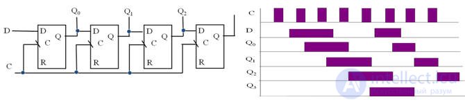
Parallel RG
A parallel register performs parallel data loading, in which all data bits are entered into the register simultaneously on a single clock pulse. A parallel register can be made into a ring register, in which case information is not lost when circulated.
Write when C=1 Qi = Di C = 0
Qi is held until a new number is written
To write a new number, a "1" must be applied to C
Digital-to-analog converters (DACs) and analog-to-digital converters (ADCs)
Main parameters of DACs and ADCs
• Resolution, expressed in bits and characterizing the range of measurement of the input quantity.
• Transfer coefficient error, showing the difference between the actual and the prescribed values (in units of the least significant bit).
• Linearity of the characteristic, i.e., the presence of proportionality between the reference analog value and the code corresponding to that value, in units of the least significant bit.
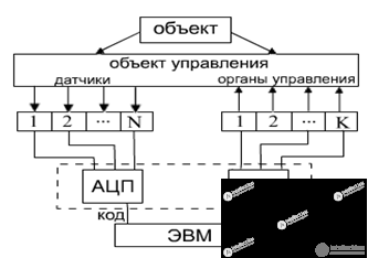
Possible applications of DACs and ADCs
Digital-to-analog converters
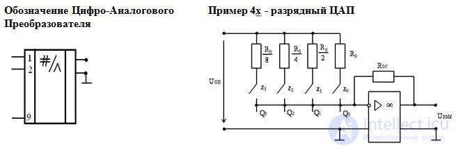
where z0, z1, z2, z3 – coefficients taking the value "0" or "1" depending on whether the corresponding switch is closed or open.
A 4-bit binary code is converted into an output voltage level in the range (0÷15) ΔU, where ΔU is the quantization step. The smaller ΔU, the greater the DAC's resolution
Analog-to-digital converters
ADC symbol
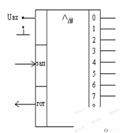
An ADC (analog-to-digital converter) is a special type of encoder.
ADC operating principle: the sequential counting method is used.
How an ADC works
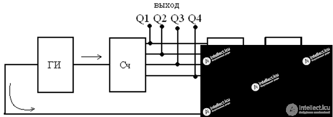
The pulse generator PG produces a sequence of pulses, which are converted into a binary code by means of the counter Ctr. This code controls the DAC's switches. The DAC's output voltage is fed to one of the comparator's inputs. When the voltages Uin and Udac are equal, the comparator issues a signal that stops the PG's operation. The output of the counter holds a binary code corresponding to the voltage Uin
Microprocessor
A microprocessor is a general-purpose digital IC (a type of LSI) capable of performing the complete set of functions of a computer's central processing unit.
With the advent of microprocessors, the need to design a new IC for each new application disappeared
Main manufacturers of modern microprocessors: microprocessor manufacturing companies: IBM, Intel- Pentium, Motorola, AMD,
продолжение следует...
Часть 1 Electronics
Часть 2 - Electronics
Часть 3 - Electronics

Comments