The simplest semiconductor devices include those made of a single semiconductor with intrinsic conductivity (see § 8-k). These are thermistors and photoresistors – devices that change their resistance depending on temperature and/or illumination. Thermoelements and photocells, as well as diodes, are somewhat more complex, since they consist of several semiconductors and no longer have intrinsic but extrinsic (impurity) conductivity. Let us examine them in more detail.
Thermistors and photoresistors do not generate electric current; they merely change their resistance to the current flowing through them. Under the influence of heat or light, the number of free electrons and holes increases, as a result of which the conductivity increases (or, equivalently, the resistance decreases). Thermoelements and photocells, on the contrary, are capable of generating electric current, that is, of being sources of electrical energy.
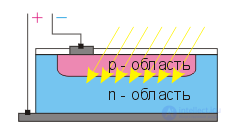
A semiconductor photocell consists of an n-type silicon crystal in which a p-region has been created by adding impurities (see figure). In § 8-k we noted that charges of opposite sign arise spontaneously at the ends of a p-n junction. That is, it can be regarded as a source of short-lived current. If, however, light energy is continuously supplied to the p-n junction (that is, causing more and more electron-hole pairs to form), the result is a continuously acting source with a voltage of about 1 V.
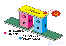
A semiconductor thermoelement consists of two semiconductors, p-type and n-type, that do not form a p-n junction (see figure). They are joined by a metal plate, to which heat is supplied from a heater (shown in yellow). The other ends of the semiconductors touch separate metal contacts, which are cooled by air or some other means (shown in green). In the colder parts of the semiconductors, the number of free electrons and holes decreases, since at a lower temperature «impurity» electrons leave their atoms less often, and so holes form less often too.
Semiconductor devices: thermistors and photoresistors, thermoelements and photocells, diodes and triodes (transistors). The operating principle of any semiconductor device is based on the dependence of the semiconductor's properties on external conditions: heating, illumination, contact with other semiconductors.
Self-check questions
- The simplest semiconductor devices are those that ...
- More complex semiconductor devices are made from ...
- Why can photoresistors and thermistors change their resistance?
- Unlike thermistors and photoresistors, ...
- Describe the construction of a semiconductor photocell. It ...
- Any p-n junction can be a source of short-lived current, because ...
- To obtain a long-acting source of current, one must ...
- The p-type and n-type semiconductors in a thermoelement ...
- For a semiconductor thermoelement to be a source of electrical energy, ...
- Why does cooling the lower ends lead to a decrease in the number of free charges?
Under the action of heat, at the upper ends of the semiconductors, on the contrary, the number of free electrons and holes increases. Repelled by their «brothers» or «sisters», they move into the lower parts of their crystals, charging them with opposite signs. Strictly speaking, having two semiconductors is not obligatory, since they do not touch each other. A pair of semiconductors is used to create opposing flows of electrons and holes, that is, a higher voltage. In addition, the heat obtained from the energy source is used more fully, which also leads to a significant increase in the efficiency of the thermoelement.
Thermistors and photoresistors are used as sensors of temperature and illumination, allowing these characteristics to be measured by electronic instruments. This makes it possible to automate measurements and, as a result, technological processes. Thermoelements and photocells are used as the main sources of electrical energy in hard-to-reach places on the Earth's surface and in space, as well as alternative, environmentally clean sources of electricity.
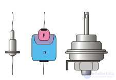
A semiconductor diode (see figure) is a device with a single p-n junction and two contacts for inclusion in a circuit. Diodes are used to pass current in only one direction, which is necessary for converting alternating current into direct current (see § 9-y), as well as for detecting radio signals (see § 11-y).
As a rule, diodes are made from a germanium or silicon crystal with n-type conductivity. A drop of indium is fused into one of the surfaces of the crystal. As a result of the diffusion of indium atoms deep into the base crystal, a p-type region forms within it. The rest of the crystal retains n-type conductivity. A p-n junction, capable of passing direct electric current in only one direction, arises between them. Its application – in the next section.
Self-check questions
- How does a larger number of free charges arise at the upper ends?
- The «thermal» electrons and holes that arise in the upper parts of the semiconductors ...
- Why are two semiconductors of different types used in a thermoelement?
- How are thermistors and photoresistors used in science and technology? They ...
- How are thermistors and photoresistors used in everyday life around us? They ...
- A semiconductor diode is a device ...
- In electrical circuits, diodes are used ...
- In addition to detecting radio signals, this property of diodes is needed ...
- When a drop of indium is fused into an n-type silicon or germanium crystal, ...
- Between the resulting p-region and the main part of the crystal ...
See also
- Diode
- Transistor
- Integrated circuit
- Processor
- Peltier element
- [[b278]]
See also


Comments