Lecture
Since the radio frequency amplifier is located at the input of the receiving device, its noise characteristics and dynamic range basically determine the characteristics of the device as a whole. It is the noise factor of the radio frequency amplifier that determines the sensitivity of the radio receiver. The non-linear properties of the amplifier are estimated by the characteristics IP2 and IP3. To ensure high linearity in all cascades of the receiver class A amplifiers are used. A very important parameter is the 1 dB point of compression.
In connection with the microminiaturization of modern element base and the associated miniaturization of radio receiver units, it is now possible to use circuit solutions that were previously used at much lower frequencies at the microwave. This is due to the fact that the dimensions of the block relative to the wavelength of the working oscillation become less than one tenth of the wavelength and as a result, when developing this block, we can neglect the wave effects during the propagation of oscillations.
At high frequencies, the best characteristics of the circuit has a transistor with a common base. In this circuit, the transistor has the best linearity due to internal feedback. In addition, its frequency response is expanding. The low pass capacity of the collector-emitter does not create conditions for parasitic self-excitation of the amplifier circuit.
An additional increase in the stability of the circuit is achieved by the inclusion of low-pass filters at the input and output of the transistor cascade. These filters are designed for the entire frequency band in which the transistor retains the amplifying properties. As a result, the phase balance is not performed over the entire frequency range and self-excitation becomes impossible. The same filter converts the input and output resistance of the transistor to a standard resistance of 50 Ohms. Input and output capacity is included in the filter. An example of such a radio frequency amplifier circuit is shown in Figure 1.
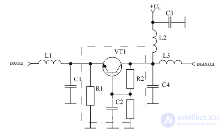
Figure 1. Schematic diagram of a radio frequency amplifier with 50 Ohm input and output impedance on a common base transistor
In this circuit, the resistors R1 ... R3 realize the emitter stabilization of the operating mode of the transistor in direct current. Capacitor C2 provides a high frequency ground to the base of the transistor, and capacitor C3 filters the noise supply circuits. The inductor L2 is the collector load of the transistor VT1. It passes the supply current to the collector circuit of VT1, but at the same time decouples the alternating current power source of the radio frequency. Low-frequency filters L1, C1 and C4, L3 provide a transformation of the input and output impedance of the transistor to 50 Ohms. The applied low-pass filter circuit allows you to include in its input or output capacitance of the transistor. The input capacitance of the transistor VT1 together with the capacitance C1 forms the input filter of the amplifier, and the output capacitance of the same transistor together with the capacitance C4 forms the output filter of the low frequency.
Another common radio frequency amplifier circuit is a cascode amplifier. In this circuit, two transistor cascades are connected in series - with a common emitter and with a common base. This solution allows you to further reduce the value of the pass-through capacitance of the amplifier. The most common cascode amplifier circuit is a circuit with galvanic coupling between transistor cascades. An example of a cascode radio frequency amplifier assembled with bipolar transistors is shown in Figure 2.
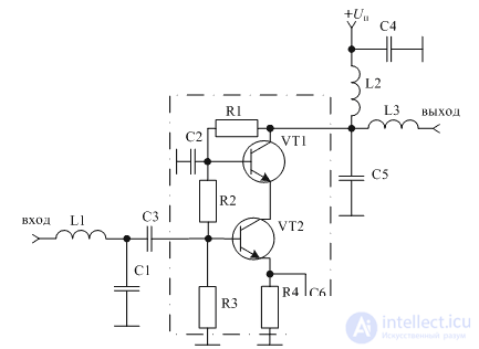
Figure 2. Schematic diagram of a cascode radio frequency amplifier
In this circuit, just like in the circuit shown in Figure 1, the emitter stabilization circuit of the operating point of the transistor VT2 is applied. Capacitor C6 eliminates negative feedback at the frequency of the received signal. In some cases, this capacitor is not set to increase the linearity of the amplifier and to reduce the gain of the radio frequency amplifier.
Capacitor C2 provides the grounding of the base transistor VT1 AC. Capacitor C4 filters the AC power supply. Resistors R1, R2, R3 determine the operating points of transistors VT1 and VT2. Capacitor C3 decouples the base circuit of the transistor VT2 at a constant current from the previous stage (input bandpass filter). The load on the AC collector circuit is the L2 choke. As in the radio frequency amplifier circuit with a common base at the input and output of the cascode amplifier, low-pass filters are used. Their main purpose is to provide a transformation of the input and output impedance in the value of 50 Ohms.
Please note that to connect the input voltage and the supply voltage, as well as to remove the output amplified voltage, three pins of the circuit are sufficient. This allows you to perform an amplifier in the form of a chip with literally three pins. Such enclosures have minimal dimensions, and this allows to avoid wave effects even at sufficiently high frequencies of the working signal.
Currently, radio frequency amplifier circuits are produced by a number of companies in the form of ready-made microcircuits. For example, such chips as RF3827, RF2360 from RFMD, ADL5521 from Analog Devises, MAALSS0038, AM50-0015 from M / A-COM. In these chips are used arsenide-gallium field-effect transistors. The upper amplified frequency can reach 3GHz. In this case, the noise figure ranges from 1.2 to 1.5 dB. An example of a schematic diagram of a radio frequency amplifier using an integrated microcircuit MAALSS0038 of the company M / A-COM is shown in Figure 3.
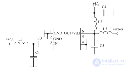
Figure 3. Schematic diagram of a radio frequency amplifier using an integrated circuit MAALSS0038
RF signals in the range of hundreds of megahertz to a few units of gigager can be amplified only if the dimensions of the microcircuits are very small and the design of the printed circuit board is carefully studied. That is why all the manufacturers of radio frequency amplifiers give examples of printed circuit boards. An example of the design of a printed circuit board of a radio frequency amplifier assembled on a MAALSS0038 chip from M / A-COM is shown in Figure 4.
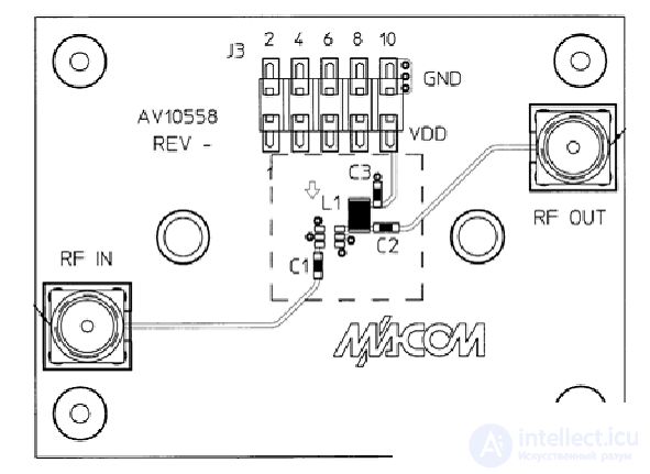
Figure 4. Radio Frequency Amplifier PCB Design
The board clearly shows the use of microstrip lines to apply the radio frequency voltage to the chip of the cascode amplifier and to transfer the amplified voltage to the next stage. Dimensions of all parts designed for surface mounting are minimal. This avoids wave effects and significantly reduces the parasitic parameters of these parts.
It should be noted that often between the output of the radio frequency amplifier and the input of the frequency converter is often put a filter similar to the input filter, as shown in Figure 2 [Superheterodyne receiver]. It allows you to increase the suppression of side channels formed in the frequency converter. Since the input impedance of the filter and the output impedance of the radio frequency amplifier are 50 Ohms, their conjugation usually does not cause problems.

Comments
To leave a comment
Devices for the reception and processing of radio signals, Transmission, reception and processing of signals
Terms: Devices for the reception and processing of radio signals, Transmission, reception and processing of signals