Equivalent circuit amplifying device.
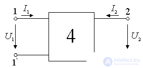
In the mode of small signals, a transistor or a lamp can be represented by an active linear quadrupole with a dependent current generator.

Figure 9.4.
Such a quadrupole is described by two linear equations connecting the voltages and currents at its input and output. Positive directions of currents and voltages are indicated in the figure by arrows. We will use the system of y-parameters, since at high frequencies it is most convenient. In the system of y- parameters, the equations of the quadrupole are:
 .
.
Recall that the y- parameters are determined during a short circuit at the input and output:
 - input conductance of a quadrupole with a short circuit at the output;
 - reverse conduction at input short-circuit;
 - direct conduction at short-circuit at the output (slope);
 - output conductance at the input short-circuit.
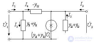
The analysis of specific amplifier circuits is more illustrative if we use the equivalent circuits obtained on the basis of the theory of two-port networks. The most common is the following equivalent circuit amplifying device.

Figure 9.5.
For further analysis, y- parameters are conveniently presented in the form:
 ;
;  ;
;
 ;
;  .
.
Where  ;
;  - the frequency at which
  i.e. slope decreases in
  time.
time.
 where
where  .
.
Equivalent amplifier circuit.
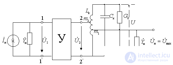
The complete equivalent circuit of the amplifier contains the signal source and load.

Figure 9.6.
For this scheme
 ;
;
 the sign "-" in this expression appears due to the fact that the voltage on the load of the quadrupole (at points 2-2 ') from the current
  will be opposite in sign to stress
  ;
;
Where  - the total conductivity of the circuit and the load, converted to the output of the quadrupole, i.e. to points 2-2 '.
The diagram shows the incomplete inclusion of the contour. Inclusion rates
 ;
;  .
.
The main characteristics of the amplifier.
We define the main characteristics of the amplifier. Cascade ratio
 ;
;
 ;
;
 ;
;
 .
.
Attitude  find from the second equation of the quadrupole
 .
.
Substitute here 
 ,
,
from here
 .
.
Substitute the resulting relation in the expression for
 .
.
or if we substitute the value 
 ,
,
Where  - total equivalent circuit conductivity.
The total equivalent conductivity of the circuit can be expressed in terms of the equivalent resonant conductivity of the circuit and the generalized detuning
 ;
;
 ,
,
 - equivalent resonant conductivity of the circuit;
 - generalized detuning.
Then
 .
.
Gain module
 .
.
With  find the resonance gain
 .
.
Insofar as  depends on the coefficients
  and
and  then there should be optimal values of these coefficients for which
  will be the maximum.
Expression research for  maximum allows to find the optimal values of the coefficients
 ;
;
 ,
,
Where  .
.
Substituting the values obtained  in the expression for
  find the maximum gain
 .
.
It is clear from the last expressions that the resonant gain reaches its maximum value with the same contour shunting on the output side of the active element of this stage and on the load side, i.e. when
 .
.
Expression for  shows that with a small proper (constructive) attenuation of the contour, i.e. at D >> 1, the gain reaches its limit for the active element value
 .
.
If the structural attenuation of the contour is large, close to the equivalent, given from the condition of obtaining the required selectivity, then the gain is small, because at  ,
,  . Hence it is clear that the contour should be sought to perform with the least possible own attenuation.
We derive the equation of the resonant curve of the amplifier:
 .
.
Those. the resonant characteristic of the amplifier in addition to the actual resonant properties is affected by the dependence of the coefficients  ,
,  and toughness
  from disorder. At small detuning, the change can be neglected.
  ,
,  and
and  . Then
 .
.
From here you can find the bandwidth of the amplifier for a given non-uniformity  .
.
 .
.
With 
 .
.
Phase characteristic of the amplifier has the form
 .
.
Let us determine the input conductance of the amplifier stage (at points 1-1 'of the full equivalent circuit).
From the first equation of the quadrupole we get
 .
.
Substituting here the value we found earlier  get
get
 (+)
(+)
or, given that  and
and  get
get
 .
.
In the resulting expressions for  the second term is due to the conductivity of the internal feedback of the active element
  .
.
Similarly, you can find the output conductivity of the active element (at points 2-2 'full equivalent circuit):
 . (*)
. (*)
The structure of the expressions (+) and (*) is the same due to the equations of the quadrupole with respect to the input and output voltages and currents. From the obtained expressions it is clear that due to the internal OS, due to conductivity  , input conductance depends on the conductivity of the load, and output - on the conductivity of the signal source.


Comments
To leave a comment
Devices for the reception and processing of radio signals, Transmission, reception and processing of signals
Terms: Devices for the reception and processing of radio signals, Transmission, reception and processing of signals