
Lecture
Even after the advent of digital computers, computation and signal processing were often carried out using analog electronics. Operational amplifiers formed the basis of these devices.
Operational amplifiers as a class emerged as standardized elements of analog computers (AVMs) after World War II. They were used to build stages performing mathematical operations: addition, subtraction, integration, differentiation, and so on. The word "operational" in the name arose from this fact. Voltage was used as the input signal.
Computations could be fairly complex and require a large number of stages, which imposed fairly strict requirements on the standardization and stability of the characteristics of operational amplifiers. Meeting the requirements for characteristic stability was achieved by introducing negative feedback (NFB) stages into the circuits. External feedback was used for standardized operational amplifiers. The characteristics of such a stage were determined solely by the parameters of the feedback loop.
Mass application of operational amplifiers began in the second half of the 1960s, when serial production of relatively inexpensive integrated op-amps was established. The use of operational-amplifier chips then became economically viable, first in industrial electronics, and later in consumer electronics as well.
The featured image used is a photograph of the Soviet counterpart of the LM101 operational amplifier, one of the first mass-produced integrated op-amps.
Operational amplifier (op-amp) - is an electronic amplifier that has two inputs and one output. It is used to amplify electrical signals, as well as to create various electronic circuits.
The main characteristics of an op-amp are gain, input resistance, output resistance, bandwidth, nonlinearity coefficient, and others. Depending on the task to be solved, an op-amp with specific characteristics can be chosen.
An op-amp usually consists of an input stage, a gain stage, and an output stage. The input stage provides high input resistance, which allows the op-amp to amplify weak signals. The gain stage provides high signal amplification, while the output stage provides low output resistance, which allows the op-amp to drive the load.
Op-amps are widely used in electronics for signal amplification, summation, filtering, demodulation, and other applications. They can also be used to create precision reference voltage sources, integrators and differentiators, as well as to solve automatic control problems.
Typically, an operational amplifier has two inputs, an inverting input and a non-inverting input, and one output. An op-amp amplifies the voltage difference between its inputs. The open-loop gain of an operational amplifier is on the order of 104…106 (80…120 dB) for direct current.
The operating principle of an op-amp is most clearly revealed by the «ideal operational amplifier» model. The model has the following properties:
- The inputs of an ideal op-amp have no effect on the input signals and have infinitely large resistance and infinitely small capacitance.
- The output of an ideal op-amp has zero resistance and can supply any voltage and any current to the load.
- The gain of an ideal op-amp tends to infinity and does not depend on the frequency of the input signals.
- The propagation delay of the signal in an ideal op-amp is zero, and there is no phase shift.
- An ideal op-amp with feedback applied tends to establish equal voltage at its inputs.
The circuit of an operational amplifier without feedback is shown below:
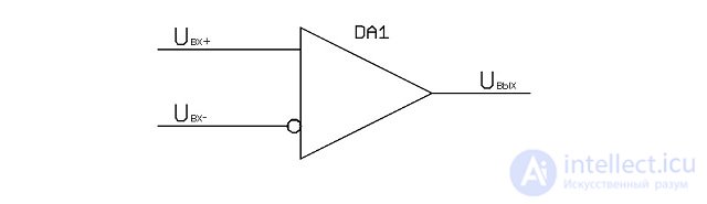
An ideal op-amp connected without feedback operates as follows: the output voltage is equal to the difference between the input voltages, multiplied by the open-loop gain of the ideal op-amp:
 |
(1) |
Let us express the difference between the input voltages of the ideal op-amp in terms of the output voltage and the open-loop gain of the ideal op-amp:
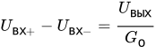 |
(2) | |
| where: | Uout – the output voltage of the op-amp; | |
| Uin+ – the voltage at the non-inverting input of the op-amp; | ||
| Uin- – the voltage at the inverting input of the op-amp; | ||
| Go – the open-loop gain of the op-amp. |
Since, according to property 3 of the ideal operational amplifier model, the gain Go tends to infinity, we obtain confirmation of property 5 of the model for the ideal op-amp without feedback as well:
 |
(3) |
The inverting amplifier is a proportional (gain) element. It performs the operation of multiplying the input signal by a coefficient k.
The amplifier is covered by negative DC feedback. The feedback network consists of a voltage divider built from resistors R1 and R2:
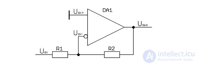
From property 5 of the model it follows that the voltage at the inverting input of the op-amp Uin- is equal to the voltage at the non-inverting input Uin+. Since the non-inverting input of the op-amp is connected to common (ground), a potential of 0 V is established at the inverting input.
According to property 1 of the ideal operational amplifier model, the inverting input draws no current; consequently, the voltage drop across resistor R1 equals the voltage Uin, the voltage drop across resistor R2 equals the voltage Uout, and the currents through the divider resistors are equal.
We obtain the following relation:
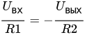 |
(4) |
from which it follows that:
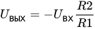 |
(5) | |
| where: | Uout – the output voltage of the inverting amplifier; | |
| Uin – the input voltage of the inverting amplifier; | ||
| R1, R2 – the resistances of the resistors in the feedback network of the inverting amplifier. |
According to formula (5), the gain of the inverting amplifier is:
 |
(6) |
From formula (6) it can be seen that the gain of an ideal inverting amplifier can range from 0 to — ∞.
The input impedance of an ideal inverting amplifier is equal to the resistance of resistor R1, since, according to property 1 of the ideal op-amp model, the inputs do not draw current, and the inverting input is held at a potential of 0 V according to property 5.
When the resistances of the resistors in the feedback loop are equal, we get an inverting follower.
When the ratio of the resistor resistances is R1 > R2, the circuit works as an inverting attenuator, i.e. it begins to «attenuate» the input signal.
The non-inverting amplifier, like the inverting amplifier, is a proportional element. It performs the operation of multiplying the input signal by a coefficient k.
The amplifier is covered by DC negative feedback. The feedback loop consists of a voltage divider built from resistors R1 and R2. The signal from the voltage divider is fed to the inverting input:
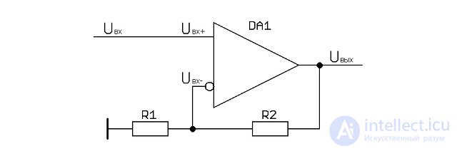
From property 5 of the model it follows that the voltage at the inverting input of the op-amp Uin- is equal to the voltage at the non-inverting input Uin+. In this case Uin+ is equal to the input voltage Uin.
According to property 1 of the ideal operational amplifier model, the op-amp inputs draw no current, consequently the voltage drop across resistor R1 is equal to the voltage Uin, and the voltage drop across the series-connected voltage-divider resistors R1 and R2 is equal to the voltage Uout.
We obtain the following relationship:
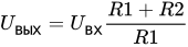 |
(7) | |
| where: | Uout – is the output voltage of the non-inverting amplifier; | |
| Uin – is the input voltage of the non-inverting amplifier; | ||
| R1, R2 – are the resistances of the resistors in the feedback loop of the non-inverting amplifier. |
According to formula (7), the gain of the non-inverting amplifier is:
 |
(8) |
From formula (8) it can be seen that the gain of an ideal non-inverting amplifier cannot be less than unity.
The input impedance of an ideal non-inverting amplifier is equal to the impedance of the non-inverting input, which, according to property 1 of the ideal op-amp model, tends to infinity.
A special case of the op-amp non-inverting amplifier circuit is the follower circuit, where the resistance R1 = ∞, and R2 = 0:
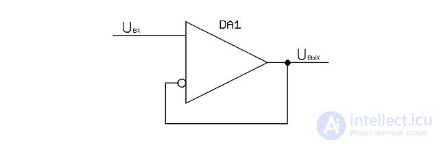
The circuit has a high input and a low output resistance, which allows, for example, a high-impedance signal source to be matched with a low-impedance load.
Both amplifier circuits, the inverting and the non-inverting, are proportional elements performing the operation of multiplying the input signal by a coefficient k.
The fundamental differences between the circuits are that:
Based on the above, inverting amplifiers should be used in circuits requiring matching with low-impedance signal sources, while non-inverting amplifiers should be used for matching with high-impedance signal sources, as well as at the inputs of measuring devices to minimize the effect on the measured signal.
Increasing the input resistance of an inverting amplifier via resistor R1 requires a proportional increase of resistor R2's resistance by the gain factor k. Excessive increase of resistor R2's resistance can be prevented by using a T-network in the amplifier's feedback circuit:
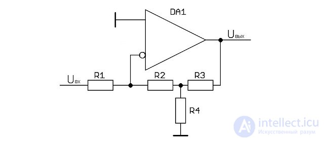
The gain of an inverting amplifier with a T-network:
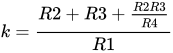 |
(9) |
The input resistance of an inverting amplifier with a T-network is approximately equal to the resistance of resistor R1.
At k = 10 and a resistance R1 = 500 kΩ, in an inverting amplifier circuit with a voltage divider in the feedback loop, the resistance of resistor R2 must be 5 MΩ.
In the case of an inverting amplifier with a T-network, at k = 10, a resistance R1 = 499 kΩ and a resistance R4 = 100 Ω, the resistance of resistors R2 and R3 will be equal to 22.6 kΩ. The calculation of the feedback circuit is more complex in this case, but using a T-network in the feedback circuit at large values of resistor R1's resistance provides more stable operation of the amplifier.
In the previous article of this series, we became acquainted with the model of an ideal operational amplifier and learned how to build a proportional (amplifying) stage using an ideal operational amplifier.
In this article of the series we will look at the differences between a «real» operational amplifier and an «ideal» one, become acquainted with the limitations of a real op-amp resulting from these differences, and learn about the main characteristics of real operational amplifiers.
The cover image shows the K140UD708 chip, the Soviet analog of the «classic» 741-series op-amps, and the K574UD2B, an analog of the popular TL083 op-amp.
An integrated operational amplifier is a fairly complex device, but its operation can be explained and its main characteristics described even using simplified models.
To understand the characteristics of an op-amp in the «static state», let us turn to the low-frequency equivalent circuit of the operational amplifier shown in Figure 1.1 on page 6:
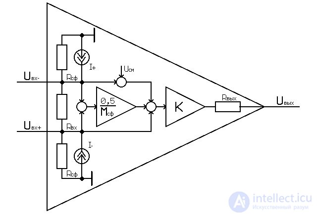
The main element of an op-amp is an inertia-free proportional stage with a gain of K. The voltage from the output of this stage is fed to the op-amp's output through resistor Rout.
The datasheet usually specifies the following op-amp characteristics:
— Gain: an op-amp characteristic numerically equal to the transfer coefficient K at DC or frequencies below 10 Hz.
— Output resistance: an op-amp characteristic numerically equal to Rout of the equivalent circuit with the feedback loop open.
Voltages Uin+ and Uin- are applied to the op-amp's inputs. The inputs have finite resistance and can draw current, which is different for each input.
Let us formulate property 1 for a real operational amplifier:
1. The inputs of a real op-amp have finite impedance, can draw current and thus affect the input signal.
If the non-ideality of an op-amp «at the inputs» is largely determined by technological limitations, then the non-ideality «at the output» is also affected by limitations imposed by the power supply.
Property 2 for a real op-amp, taking into account power supply limitations:
2. The output of a real op-amp has non-zero resistance and can provide a limited voltage range at a limited load current.
Also, the op-amp's datasheet always specifies:
— Rated supply voltage
— Range of output voltages
— Load resistance
Let us illustrate the parameters discussed using the example of the K140UD708 operational amplifier.
This op-amp is designed to operate from a dual-polarity supply voltage of UP = ± 15 V and can provide an output voltage range of Uout = ± 10.5 V into a load resistance of RL = 2 kΩ. The load capacitance must not exceed 1000 pF. The gain of the K140UD708 op-amp at a frequency of 5 Hz with UP = ± 15 V, Uout = ± 10 V and RL = 2 kΩ is 30000.
Let us return to the input-circuit parameters:
— Common-mode input voltage range: the range of allowable input voltages on the op-amp's inputs when tied together. Usually lies within the range of the supply voltage.
— Differential input voltage: the range of allowable input voltages between the op-amp's inputs. Can range from a fraction of a volt up to the voltage of a single-polarity supply (or the two supply voltages for a dual-polarity supply).
Applying voltages outside these ranges to the inputs of a real operational amplifier can cause the op-amp to fail.
— Input resistance: the resistance of an input, measured with 0 V applied to the other input. Denoted Rin on the equivalent circuit. May be called the «input resistance for the differential signal». For op-amps with bipolar-transistor inputs it can be 103 – 106 Ω or more. The input resistance of inputs on field-effect transistors is significantly higher.
— Common-mode input resistance: denoted on the equivalent circuit as two resistors of resistance Rcm, connected in parallel with the current sources I+ and I-. Usually exceeds the value of Rin by one to two orders of magnitude.
— Input current: the arithmetic mean of the sum of the input currents, denoted on the equivalent circuit as two current sources I+ and I-, measured at the value of Uin such that Uout = 0. The input current can change with changes in the supply voltage and the load resistance.
— Input offset current: the absolute value of the difference between the currents flowing into each input at the value of Uin such that Uout = 0. It characterizes the «asymmetry» of the inputs caused by manufacturing factors.
— Offset voltage: the value of the voltage difference Uos = (Uin+ – Uin-) at the inputs of the operational amplifier at which the output voltage Uout = 0. Since Uos can have either sign, on the equivalent circuit it is added in series with Uin-.
— Common-mode rejection ratio: on the equivalent circuit, common-mode rejection is implemented by an instantaneous proportional element, to whose input the voltage difference (Uin+ – Uin-) is applied. The gain of this element is (0.5 / Mcm). The higher Mcm is, the less a change in the common-mode signal affects the output voltage of the op-amp.
The main difference between a real op-amp and an ideal one is that, «dynamically», a real op-amp behaves like a low-pass filter (LPF).
From this, properties 3 and 4 of a real operational amplifier can be formulated as follows:
3. The open-loop gain of a real op-amp can be 104 – 106 (80 — 120 dB) at low frequencies and decreases as frequency increases.
4. The propagation delay of the signal in a real op-amp is not equal to zero; in terms of voltage, the phase of the output signal lags behind the phase of the input signal.
Let us consider two of the most important dynamic characteristics of a real op-amp:
— Unity-gain frequency: the frequency (Hz) at which the op-amp's gain equals unity.
— Maximum output voltage slew rate: a characteristic (V/µs) reflecting the speed of the op-amp's response to a rectangular pulse at the input.
Let us examine the difference between a real op-amp and an ideal one «in dynamics» using the method given in section 7.1.4 on pp.86-88 .
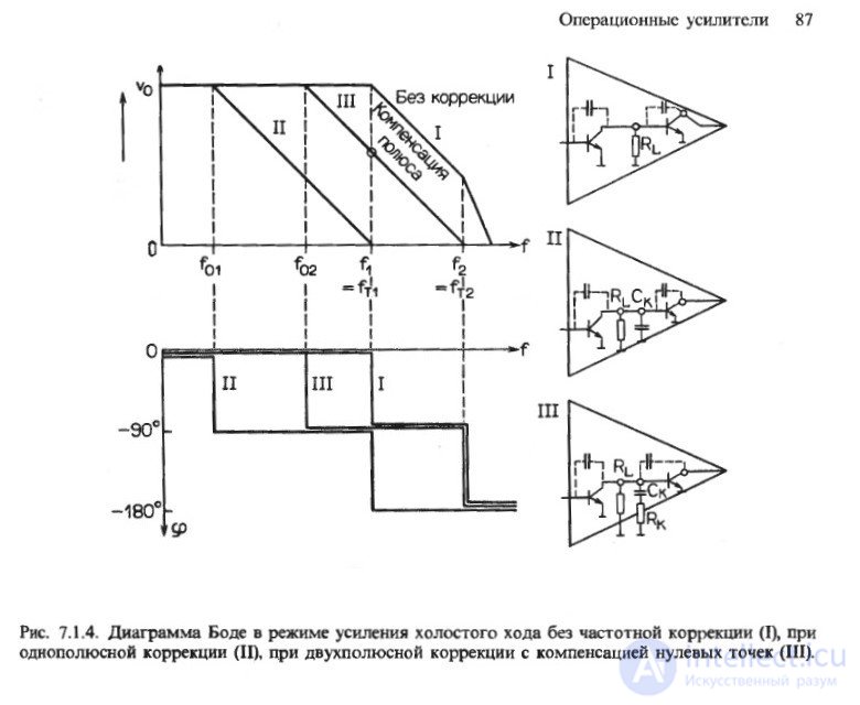
Let us examine the behavior of a real op-amp without built-in frequency compensation using the curves labeled I on the Bode plot shown above, and using equivalent circuit I.
At frequencies below f2, a real op-amp behaves as a 1st-order low-pass filter with cutoff frequency f1. The cutoff frequency f1 is determined by the characteristics of the input differential stage, represented in the equivalent circuit by a parasitic capacitor drawn with a dotted line. At frequencies in the range from f1 to f2, the real op-amp's frequency response has a slope of -6 dB per octave.
At frequencies above f2, the characteristics of the op-amp's second stage begin to affect the frequency response. At these frequencies the response has a slope of -12 dB per octave, corresponding to a 2nd-order low-pass characteristic.
The phase shift at frequencies below f1 is 0°. The phase shift in the range from f1 to f2 is -90°, and at frequencies above f2 it is -180°.
If, at frequency f2, the op-amp's gain is greater than unity (0 dB), the negative feedback becomes positive, and the op-amp enters self-oscillation.
Stable operation of a real op-amp in «dynamics» is achieved by introducing frequency compensation.
In equivalent circuit II, frequency compensation is provided by introducing a capacitor CK into the circuit. The amplitude-frequency and phase characteristics of a real op-amp with single-pole frequency compensation are shown on the Bode plot by the curves labeled II.
The essence of single-pole frequency compensation is to provide a cutoff frequency fO1 such that at frequency f1 the op-amp's gain equals unity (0 dB).
This is how the built-in frequency compensation of the «classic» 741-series op-amp was implemented. The presence of built-in frequency compensation made this series of op-amps extremely popular. The unity-gain frequency f0 of such an op-amp is low — 1.0 MHz — but this has proven sufficient for many applications.
The unity-gain frequency f0 can be raised using two-pole («lead») compensation. In equivalent circuit III, two-pole compensation is provided by introducing a resistor RK into the circuit, connected in series with the capacitor CK. The amplitude-frequency and phase characteristics of a real op-amp with two-pole frequency compensation are shown on the Bode plot by the curves labeled III.
The «lead» frequency compensation network provides a 6 dB boost in the frequency response at frequencies above f1. The cutoff frequency fO2 is chosen so that the op-amp's gain equals unity at frequency f2.
It should be noted that introducing frequency compensation increases the stability of the op-amp stage owing to the greater inertia of that stage, and, consequently, a reduction in the output voltage slew rate.
Modern technology makes it possible to produce inexpensive, general-purpose rail-to-rail op-amps that do not require external «support circuitry» in the form of frequency compensation and zero-correction networks. The permissible ranges of the input signals (common-mode and differential) and the output signal range of such op-amps are usually equal to the supply voltage.
At present, many manufacturers produce a large number of different op-amps with varying parameters, which must be checked against the manufacturer's datasheet when selecting an op-amp.
Let us focus on the limitations that hold true for the vast majority of existing op-amps.
A real op-amp, when the negative feedback is disconnected, goes into saturation mode owing to its high gain and the presence of bias currents.
As with an ideal operational amplifier, the characteristics of circuits built with real op-amps are determined by the parameters of the feedback network. The feedback network must be designed so that, for any input voltage value within the operating range, the op-amp's output stage does not enter saturation mode.
To reduce the effect of the op-amp's input and output resistance on the parameters of the feedback circuit, the values of resistors R1 and R2 must be selected so that:
— the resistance R1 is greater than the op-amp's output resistance Rout;
— the resistance R2 is less than the input resistance Rin.
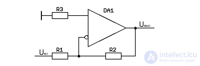
To compensate for the bias current, the op-amp's non-inverting input is connected through resistor R3 with a resistance equal to the resistance of R1 and R2 connected in parallel. This is necessary for op-amps with a bipolar-transistor input stage and is not required for op-amps with a field-effect-transistor input stage.
Circuit of an inverting amplifier with bias current compensation:
Circuit of a non-inverting amplifier with bias current compensation:
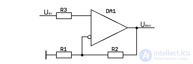
The resistances of resistors R1 and R2 for op-amps with bipolar-transistor inputs are usually chosen in the range from 2 to 100 kΩ so that the resistance of resistor R3 lies in the range from 2 to 10 kΩ. If the resistance R2 is chosen in units of MΩ, be prepared for the op-amp with such feedback circuits to operate unstably.
The input resistance of an inverting amplifier built on a real op-amp is approximately equal to the resistance of resistor R1.
The input resistance of a non-inverting amplifier built on a real op-amp is approximately equal to the common-mode input resistance Rcm of the operational amplifier.
Also, when calculating the feedback circuit, the frequency range must be taken into account. The figure below shows an example of the dependence of the operating frequency range on the gain of an op-amp stage:
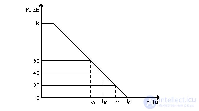
As can be seen from the graph, as the gain increases, the operating frequency range narrows. That is, an op-amp stage can provide k = 1 (0 dB) at frequencies below f0, k = 10 (20 dB) at frequencies below f20, and so on.
In addition to all of the above, a real op-amp is affected by the environment and has a temperature drift of its parameters, a dependence on power supply instability, limitations on heat dissipation, and so on.
In this article of the series, we will learn how to perform addition and subtraction operations using an op-amp. In addition, we will examine the operation of integrating and differentiating stages, as well as sample-and-hold circuits.
To the group of operational amplifiers K140UD708 and K574UD2B, the cover image adds the precision op-amp K140UD1408 – a Soviet analog of the LM308.
For those who have joined recently, I should mention that this is the third of seven articles in the series. The contents of the articles, with links to them, are given at the end of the article.
The addition operation on an op-amp can be performed using a summing amplifier. The simplest summing amplifier can be obtained by adding a resistor to the circuit of an inverting amplifier on an op-amp:
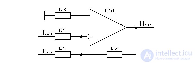
Further, the procedure is similar to the method for calculating the transfer characteristic of an inverting amplifier. The inverting input of the op-amp is at a potential of 0 V. The sum of the input currents through the input resistors, resulting from the presence of voltages Uin1 and Uin2 at the inputs, is compensated by the current through feedback resistor R2. The voltage drops across the input resistors are numerically equal to Uin1 and Uin2, and the voltage drop across resistor R2 equals Uout.
The transfer characteristic of the simplest summing amplifier, with the input resistors' resistances being equal, can be represented by the formula:
 |
(10) | |
| where: | Uout – voltage at the output of the summing amplifier; | |
| Uin1, Uin2 – voltage at the inputs of the summing amplifier; | ||
| R1 – resistance of the resistors at the inputs of the summing amplifier; | ||
| R2 – resistance of the resistor in the feedback circuit of the summing amplifier. |
The resistance of resistor R3, connected to the op-amp's non-inverting input to compensate for the bias current, is equal to the resistance of the resistors in the feedback circuit connected in parallel.
For the summing stage to operate correctly, the signal sources must have as low an output resistance as possible, so that the low input resistance of the stage does not affect the calculation result, and so that the signal sources do not shunt one another.
Subtraction with an op-amp can be performed using a differential amplifier. The differential (subtractor) amplifier circuit can also be obtained by modifying the op-amp inverting-amplifier circuit:
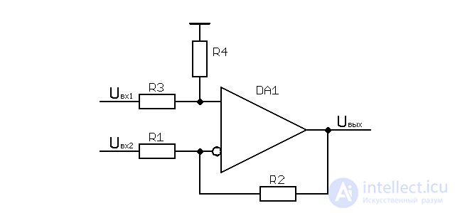
For the signal Uin1, the circuit behaves as a non-inverting amplifier, and for the signal Uin2 – as an inverting one. The transfer characteristic of the simplest differential amplifier, provided the resistances are pairwise equal (R1 = R3 and R2 = R4), can be expressed by the formula:
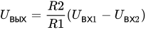 |
(11) | |
| where: | Uout – voltage at the output of the differential amplifier; | |
| Uin1, Uin2 – voltage at the inputs of the differential amplifier; | ||
| R1, R2 – resistances of the resistors in the feedback circuit of the differential amplifier. |
The simplest differential amplifier circuit is simple and clear, but it does not reflect the full complexity of this stage's behavior:
An instrumentation amplifier is a differential amplifier with equal input resistances and the ability to adjust the gain by changing the rating of only a single resistor in the feedback circuit:
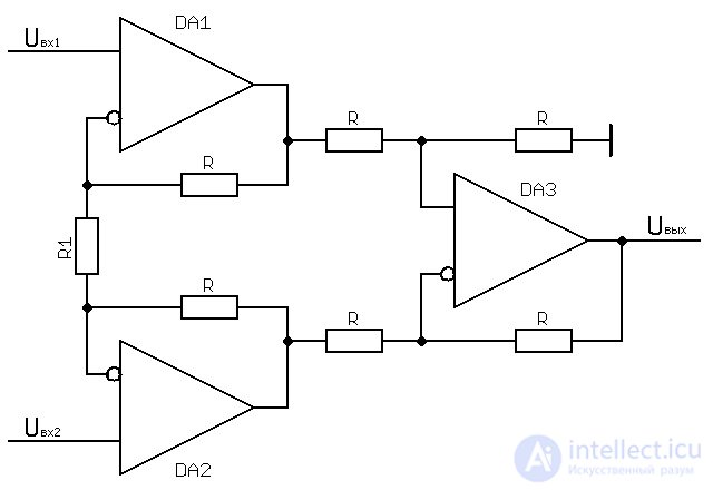
Compared with the simplest differential amplifier, the circuit is considerably more complex, but adjusting the gain comes down to selecting the resistance of only one resistor, R1. The rest of the circuit can be placed on a single chip, which improves manufacturability and simplifies ensuring equality of the resistances of the remaining resistors.
The gain of the instrumentation amplifier is calculated by the formula:
 |
(12) | |
| where: | Uout – voltage at the output of the instrumentation amplifier; | |
| Uin1, Uin2 – voltage at the inputs of the instrumentation amplifier; | ||
| R, R1 – resistances of the resistors in the feedback circuit of the instrumentation amplifier. |
The instrumentation amplifier has a number of remarkable features:
The above features make it possible to use the circuit as a universal tool. Instrumentation amplifiers are manufactured ready-made by industry. The limiting factor in the use of instrumentation amplifiers is their higher cost, so they are usually used in critical, high-budget solutions.
An integrator is designed to compute the time integral. The element has inertial (lag) behavior:
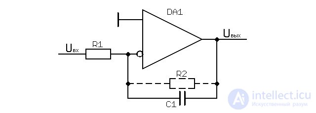
The gain of the integrator with R2 = ∞:
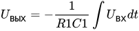 |
(13) | |
| where: | Uout – the output voltage of the integrator; | |
| Uin – the input voltage of the integrator; | ||
| R1 – the resistance of the timing-network resistor; | ||
| C1 – the capacitance of the timing-network capacitor. |
Integrators are usually designed using op-amps with field-effect-transistor inputs and negligibly small input currents, in order to minimize output-voltage drift. If the drift cannot be eliminated, a resistor R2 with a resistance on the order of units to tens of MΩ is connected in parallel with the capacitor to provide DC feedback.
Resistor R2 degrades the integrating properties of the element at very low frequencies and reduces operating stability. If the DC feedback in the integrator cannot be eliminated, it makes sense to try replacing R2 with an equivalent T-bridge, using the method given in the first publication of the series.
A differentiator is designed to compute the time derivative:
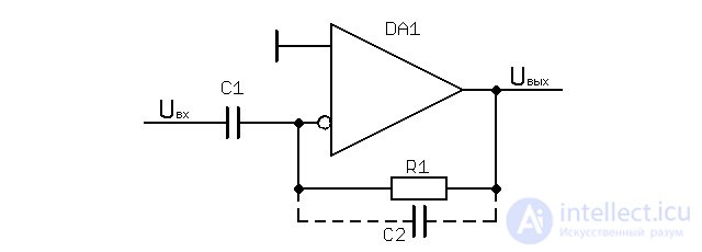
The gain of the differentiator with C2 = 0:
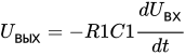 |
(14) | |
| where: | Uout – the output voltage of the differentiator; | |
| Uin – the input voltage of the differentiator; | ||
| R1 – the resistance of the timing-network resistor; | ||
| C1 – the capacitance of the timing-network capacitor. |
Differentiators are likewise designed using op-amps with field-effect-transistor inputs and negligibly small input currents. Capacitor C2 serves to reduce the element's sensitivity to high-frequency interference and to improve the stability of the element at the upper frequencies of the operating range.
Sample-and-hold circuits serve to record and store the value of an analog signal:
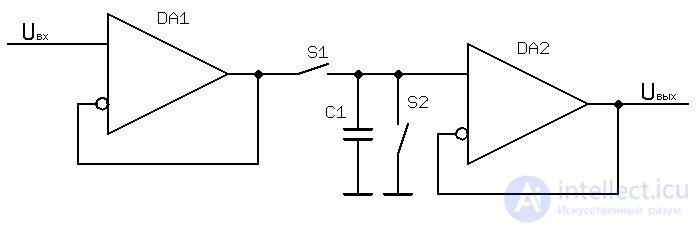
When contacts S2 close, the value stored in capacitor C1 is reset. When contacts S1 close, the value Uin is written into C1. When S1 opens, the stored value is held in C1.
A field-effect-transistor-input op-amp should be used as DA2. Capacitors with low leakage current and low dielectric absorption should be used as C1.
What unites all the elements considered in this publication is that they are used in PID controllers:
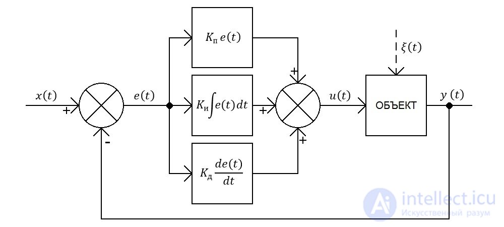
A PID controller is a device that generates a control action u(t) on the controlled object based on the error signal e(t), equal to the difference between the setpoint value x(t) and the monitored value y(t) obtained via the feedback loop.
The control action u(t) is generated according to the formula:
 |
(15) | |
| where: | Kp – the gain of the proportional element; | |
| Ki – transfer coefficient of the integrating stage, inversely proportional to the product of the resistance and capacitance of the elements of the timing chain; | ||
| Kd – transfer coefficient of the differentiating stage, directly proportional to the product of the resistance and capacitance of the elements of the timing chain. |
The circuit for forming the error signal e(t) is chosen based on accuracy requirements and budget. Often, instead of expensive integrated instrumentation amplifiers, it is more cost-effective to use circuits of the simplest difference amplifiers with carefully selected resistor values.
Since the circuits of the integrating and differentiating stages are inverting, an inverting amplifier should also be used as the proportional stage. If, in addition, the summing amplifier discussed above is used as the output summer, the controller's transfer function will exactly correspond to formula (15).
Sample-and-hold circuits are usually used to store initial or reference values of parameters. For example, a sensor's signal at the initial moment in time, and so on.
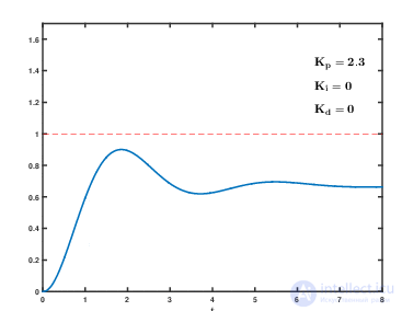
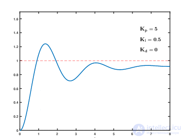
When designing a PID controller, particular attention should be paid to the method of selecting the coefficients. The most common method is tuning based on the step response (Step Response Method).
In this installment of the series, we will learn how to use op-amps to perform division and multiplication, find the absolute value, determine the sign, compare numbers, and find the largest of them. To do this, we will examine the operation of a number of op-amp circuits with transistor and diode «support components».
The article contains a large number of circuits, most of which are understandable without detailed explanations, diagrams, and graphs. Some of the solutions are given for information: they served as the basis for specialized ICs and, in their «pure form», are no longer used in modern design.
For those who have joined recently, I should mention that this is the fourth of seven articles in the series. The contents of the articles, with links to them, can be found at the end of the article.
On the cover image, alongside the family of operational amplifiers K140UD708, K140UD1408, and K574UD2B, a low-noise dual-channel op-amp K157UD2 – the Soviet analog of the LM301 – has been added.
A detector (half-wave rectifier) is designed to pass signals of only one polarity to the output. When a signal of the opposite polarity is applied to the detector's input, a level of 0 V is set at the detector's output.
A classic circuit of an active op-amp detector is shown in the figure below:
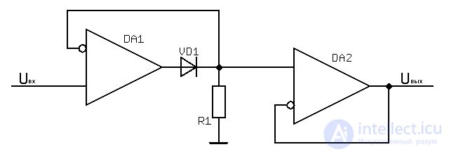
When positive values of the input signal are applied to the output (Uin > 0), the circuit behaves as a follower. The nonlinearity of the diode's volt-ampere characteristic and the magnitude of the forward voltage drop Ufwd are compensated by negative feedback. When Uin < 0, Uout = 0 V.
A significant drawback of the circuit is that DA1 enters saturation mode when a negative voltage is applied to the input: this leads to distortion of the output signal at zero crossings of the input signal.
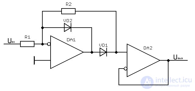
The improved active op-amp detector circuit behaves as an inverting follower for negative values of the input signal. For positive values of the input signal, due to feedback through diode VD2, a voltage equal to 2Ufwd is established at the output of the left-hand op-amp in the circuit.
A peak detector based on an operational amplifier is an electronic circuit used to measure the amplitude of peak signals. It can be used, for example, to measure the maximum amplitude of a signal within a certain time interval.
An operational amplifier (op-amp) is an electronic component used to amplify signals. It has two inputs and one output, and can be used to create various electronic circuits, including a peak detector.
[[s|peak-detect]]
A peak detector based on an op-amp can be built, for example, using a diode and a capacitor. In this case, the diode performs the function of a rectifier, and the capacitor performs the function of a storage element. The signal is taken from the diode and applied to one of the op-amp's inputs, while a reference voltage is applied to the other input. The capacitor charges up to the maximum amplitude of the signal, after which its charge is held. When the signal starts to decrease, the capacitor begins to discharge through a resistor. Thus, a voltage proportional to the maximum peak amplitude of the signal appears at the output of the op-amp.
An op-amp based peak detector can be used, for example, to measure the maximum amplitude of a signal in an audio system, to determine the power of electrical pulses, or to monitor the dynamics of light signals in optical systems.
An active peak detector serves to find the largest value of the input signal:
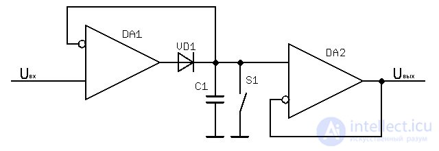
When the voltage at the circuit input is greater than that on capacitor C1, diode VD1 opens, and the voltages at the detector input and on capacitor C1 equalize. The value stored in C1 is reset by closing switch S1.
The circuit of an active signal limiter based on an op-amp is shown below:
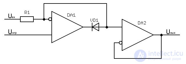
The output voltage Uout of the circuit cannot exceed the value Ulim: for values of Uin < Ulim, the input voltage Uin is fed to the non-inverting input of follower DA2. When Uin > Ulim, the voltage at the output of DA1 opens diode VD1, DA1 starts working as a follower, and the output voltage of DA2 becomes Uout = Ulim.
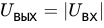
The absolute value (magnitude) of the input signal voltage is found using an active full-wave rectifier built with two op-amps:
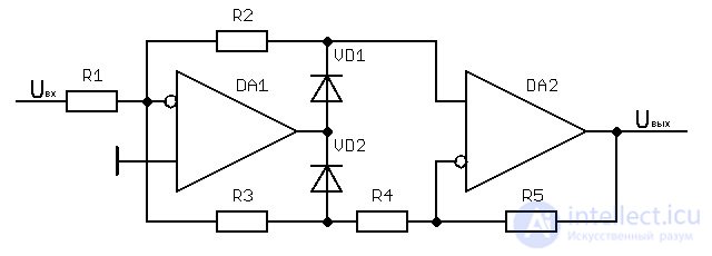
When the input voltage is negative, diode VD1 is open and the positive voltage from the output of DA1 is fed to the non-inverting input of DA2:
 |
(16) |
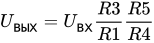
When the input voltage is positive, diode VD2 is open and the negative voltage from the output of DA1 is fed to the inverting input of DA2:
 |
(17) |
If the resistances of all resistors in the circuit are equal, we obtain:
 |
(18) |
Sometimes, when processing signals, it is necessary to multiply or divide them. In analog computing devices, multiplication and division are performed using logarithmic converters.
Before starting the logarithmic conversion, we need to extract the magnitude, for example, using an active full-wave rectifier, and determine the sign, for example, using a comparator.
Then everything works just like with the good old slide rule: the product of the absolute values (magnitudes) of the analog signals equals the sum of their logarithms, and the quotient equals their difference; squaring is equivalent to multiplying the logarithmic value by two, and taking the square root can be done by halving the logarithm.
The sum and difference of logarithms can be obtained using the summing and difference stages described in the previous publication. Multiplying by a coefficient can be done using a proportional stage (see parts one and two of the series) for K > 1, or a voltage divider for 1 > K > 0.
Converting a linear signal value into a logarithmic one can be done using a logarithmic converter. The logarithmic converter circuit shown below operates correctly with positive values of the input signal:
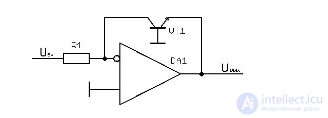
A diode can be used in the feedback loop, but using a transistor instead of a diode gives a significant improvement in temperature stability.
The reverse conversion, from a logarithmic representation to a linear one, is performed by the exponential converter circuit shown below:
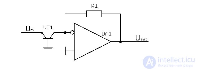
As the computing power of digital devices has increased, the topic of analog multiplication, division, and computation of the time integral and derivative has become less and less relevant. Nevertheless, specialized voltage-multiplier chips are still manufactured by industry.
The topic of multiplication and division using op-amps is covered thoroughly and in detail in Section «11.8 Analog multiplication circuits» on pp. 160–167. The mathematical apparatus is discussed in detail in Section «4.5 Voltage multipliers» on pp. 126–132. An example of using logarithmic converters as a voltage-controlled amplifier is given on p. 182 .
It should be emphasized that the transfer characteristic of logarithmic and exponential converters built on op-amps has a strong temperature dependence. Temperature compensation is required to keep the parameters of these circuits constant. A sample circuit of a logarithmic converter with temperature compensation is given in Fig. 4.94 p on p. 271 .
A comparator makes it possible to compare the input signal voltage with a reference voltage. The comparator circuit is an op-amp without feedback. In the circuit shown below, the reference voltage is applied to the non-inverting input:
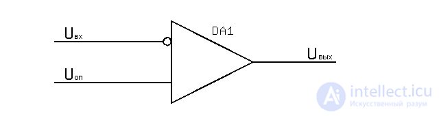
If the voltage at the inverting input is greater than the reference, the output produces a negative saturation voltage. If it is less, the output is positive.
A drawback of this circuit is the «chattering edges» effect: noise that appears at the moment of switching.
The «chattering edges» effect is eliminated by introducing a small amount of positive feedback (PFB) into the comparator circuit. The rating of resistor R1 is on the order of 100 kΩ. The circuit exhibits hysteresis and is called a «Schmitt trigger»:
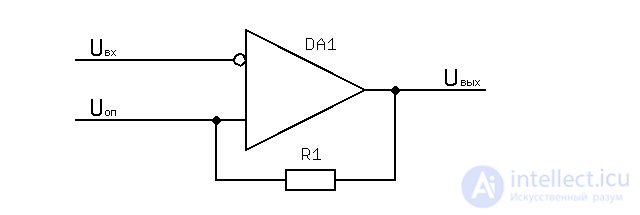
To generate digital logic-level signals, a transistor switch with an open collector (drain) is connected to the output of the comparator or Schmitt trigger.
Comparators and Schmitt triggers, including versions with single-supply power and with level shifting, are manufactured by industry in a wide range. In modern designs it is advisable to use off-the-shelf devices of this kind.
Operational amplifiers were widely used as voltage reference sources before the spread of specialized linear-regulator ICs such as the LM317 or 78xx (79xx) series. The figure below shows a stabilized voltage source circuit built on an op-amp:
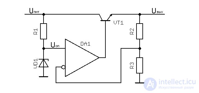
The reference voltage Uref from zener diode VD1 is applied to the op-amp's non-inverting input. The signal from voltage divider R2, R3 is applied to the inverting input. If the voltage at the inverting input is greater than Uref, transistor VT1 is turned off by the negative voltage at the op-amp's output. When the voltage at the inverting input becomes less than Uref, transistor VT1 turns on.
«Dynamically», the circuit operates as a proportional controller with an oscillatory transient response. In modern designs it is advisable to use off-the-shelf integrated linear regulators.
Below is a schematic of a stabilized current source:
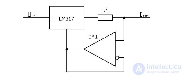
The control input of the LM317 integrated voltage regulator is fed a voltage from the op-amp output that is inversely proportional to the voltage drop across resistor R1. Since the voltage at the control input of the LM317 chip must equal 1.25 V, the output current value is calculated by the formula:
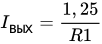 |
(19) |
Power amplifiers with
продолжение следует...
Часть 1 Operational Amplifiers: Ideal and Real, Summing Amplifier, Differentiator, Integrator, Peak Detector
Часть 2 Frequency-dependent feedback in op-amps. Active filters and signal generators on

Comments