
Lecture
Antenna effect — generally the ability of certain conductors to radiate and receive electromagnetic waves, i.e. to act as an antenna. The term is usually applied in cases where this effect is a parasitic phenomenon, i.e. electromagnetic waves are radiated or received by conductors not intended for this purpose. For example, an antenna feedercan exhibit the antenna effect if it radiates and receives electromagnetic waves.
The antenna effect (antenna effect), more formally plasma-induced gate oxide damage, is an effect that can potentially cause performance and reliability problems in the manufacture of MOS integrated circuits. Foundries ( fabs ) usually provide antenna rules , which are rules that must be followed to avoid this problem. Violation of such rules is called an antenna violation . The word antenna is used incorrectly in this context - the problem is really charge accumulation, not the usual meaning of an antenna., which is a device for converting electromagnetic fields to/from electric currents. Sometimes the phrase « antenna effect» , is used in this context, but this is less common, since there are many effects , and this phrase does not clarify what is meant.
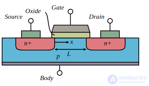
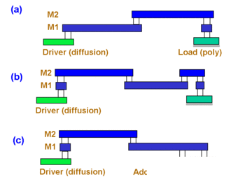
Figure 1 (a) shows a side view of a typical net in an integrated circuit . Each net will include at least one driver, which must contain a source or drain diffusion (newer technology uses implantation), and at least one receiver, which will consist of a gate electrode above a thin gate dielectric (see Figure 2 for a detailed view of a MOSFET). Because the gate dielectric is so thin, only a few molecules, breakdown of this layer is a major concern. This can happen if the net somehow acquires a voltage somewhat exceeding the chip's normal operating voltage. (Historically the gate dielectric was silicon dioxide , so most of the literature refers to gate oxide damage or gate oxide breakdown.. Since 2007 some manufacturers have replaced this oxide with various high-κ dielectric materials, which may or may not be oxides, but the effect is the same.)
Once the chip is fabricated, this cannot happen, because at least some source/drain implant is connected to every net. The source/drain implant forms a diode , which fails at a lower voltage than the oxide (either forward diode conduction or reverse breakdown), and does so in a non-destructive way. This protects the gate oxide.
However, during chip fabrication the oxide may not be protected by a diode. This is shown in Figure 1 (b), which represents a situation where metal 1 is being etched. Since metal 2 has not yet been built, the diode connected to the gate oxide is absent. Thus, if charge is somehow added to metal shape 1 (shown as a lightning bolt), it can rise to a level that breaks down the gate oxide. In particular, reactive-ion etching of the first metal layer can lead to exactly the situation shown - the metal on each net is disconnected from the original global metal layer, while plasma etching still adds charge to each piece of metal.
Gate oxide leakage, although it adversely affects power dissipation, helps avoid damage from the antenna effect. A leaky oxide can prevent charge from accumulating to the point of oxide breakdown. This leads to the somewhat unexpected observation that a very thin gate oxide is less likely to be damaged than a thick gate oxide, because as the oxide becomes thinner, leakage increases exponentially, but the breakdown voltage decreases only linearly.
Antenna rules are usually expressed as the allowed ratio of metal area to gate area. There is one such ratio for each interconnect. The area counted may consist of more than one polygon - this is the total area of all metal connected to the gates, without a connection to a source/drain implant.
Generally, antenna violations must be fixed by the router . Possible fixes include:
[[b9819]]

Comments