
Lecture
In series voltage stabilizer circuits (the modified circuit – Fig. 1, and the one using an emitter follower – Fig. 2), described above, the output resistance of the stabilizer was determined by the parameters of the emitter follower. It can be reduced even further by using a control amplifier, covered by negative feedback. Such circuits are called controlled voltage sources. The advantage of such a circuit is that the output voltage can be precisely adjusted by changing the resistance ratio; moreover, this voltage is practically independent of the  voltage of the output transistor.
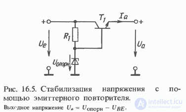
Fig. 1
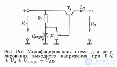
Fig. 2
The stabilizer circuit using a control amplifier has no fundamental differences from the voltage sources described in Sec. 12.1, but the current delivered to the load by the operational amplifier may prove insufficient. In this case, an additional power amplifier covered by overall feedback must be included. In principle, the circuit described in Ch. 15 can be used for such an amplifier. Since the output voltage of a power supply is always either positive or negative and never changes sign, the amplifier circuits can be simplified and limited to a single power transistor or a Darlington circuit.
Fig. 16.7 shows the circuit implementation of a stabilizer for a positive output voltage. The circuit consists of an operational amplifier connected as a non-inverting amplifier with negative voltage feedback, whose output current is amplified by an emitter follower on transistor T1. The operational amplifier is powered not by voltages symmetrical about ground, as usual, but by a single-polarity positive
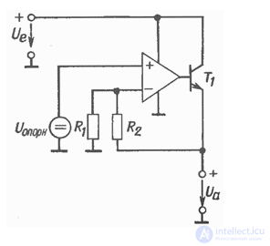
Fig. 16.7. Voltage stabilization using a control amplifier. Output voltage 
supply voltage. This imposes a restriction on the permissible range of input and output signals, which can only be positive. For power-supply circuits this restriction is of no consequence, so the use of a negative supply voltage for the operational amplifier can be dispensed with. Another advantage of such a circuit is that the positive supply voltage of the operational amplifier can be doubled without risk of exceeding its maximum permissible ratings. Thus, standard operational amplifiers can be used in stabilizer circuits with an output voltage of nearly up to 30 V.
A positive supply potential for the operational amplifier is also not mandatory if, as shown in Fig. 16.7, the unstabilized input voltage Ue is used for this purpose.
Fluctuations of this voltage have practically no effect on the stability of the output voltage, since the drift of the output voltage caused by changes in the supply voltage is extremely small in operational amplifiers.
Integrated operational amplifiers have built-in output current limiting circuits, so the base current of transistor T1 in the circuit of Fig. 16.7 is limited to the value  For this reason, the output current of the stabilizer is also limited to the value
  where B is the static current gain of transistor T1.
Since the value of this coefficient can vary considerably and increases with rising temperature, such an indirect method of limiting the output current is undesirable.
It is more convenient to use the actual output current value of the stabilizer as the current-regulating parameter. For this purpose, resistor R3 and transistor T2 are included in the circuit shown in Fig. 16.8.
If the voltage drop across R3 exceeds a value of approximately 0.6 V, transistor T2 will turn on and prevent any further increase in the base current of transistor T1. As already shown in Fig. 15.13, the value of the regulator's output current is limited to the level
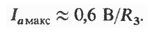
In this case, the power dissipated in output transistor T1 is equal to
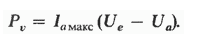
In the event of a short circuit, this power will significantly exceed the maximum permissible power for transistor T1, since the output voltage will then drop from its rated value to zero. To reduce the power dissipated by the output transistor in this case,
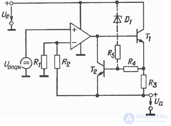
Fig. 16.8. Modified circuit for limiting the output current. Limiting value of the output current 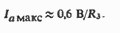
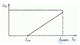
Fig. 16.9. Output characteristic of a voltage regulator with foldback current protection.
at the same time as the output voltage decreases, the current limiting level can be reduced. With this method of current limiting, the voltage regulator's output characteristic acquires a foldback (drooping) shape. It is shown in Fig. 16.9.
In the event of a significant increase in input voltage Ue, the power dissipated in the output transistor rises rapidly.
This is because the voltage difference (Ue-Ua), which enters into the power expression (16.9), increases correspondingly.
Protection of the output transistor from overheating in this case is achieved by making the current limiting level Ia max depend on the voltage difference (Ue-Ua). In the circuit of Fig. 16.8, resistor R5 and Zener diode D1 serve this purpose
If the voltage difference (Ue-Ua) remains smaller than the breakdown voltage Uz of Zener diode D1, no current flows through resistor R5.
In this case, the current limiting level remains equal to 
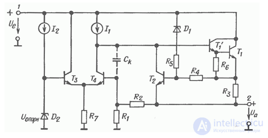
Fig. 16.10. Typical circuit of an integrated voltage regulator. 
If, however, this voltage difference exceeds the value Uz, then, owing to the formation of a voltage divider across resistors R5, R4, a positive voltage appears applied to the base-emitter junction of transistor T2. In this case transistor T2 will turn on at correspondingly smaller values of the voltage drop across resistor R3

Comments