
Lecture
Microwave loads are represented on the equivalent circuit as a two-terminal network, characterized by the reflection coefficient Γ. The scattering matrix of the load degenerates into the number s11 = Γ. Matched and reactive loads are used in microwave transmission paths.
a) b) c)
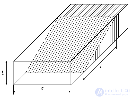
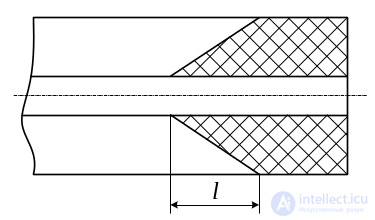
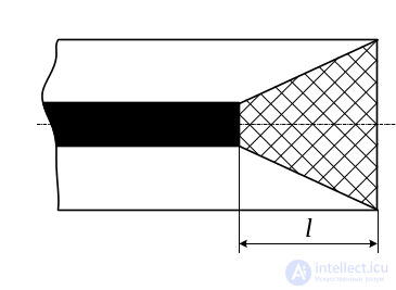
Fig. 3.1 Absorbing loads:
a – waveguide, b – coaxial, c – stripline
An ideal matched load has Γ = 0. The characteristics of real matched loads are the frequency dependence of |Γ| and the permissible absorbed power. In practice, loads with |Γ| < 0.01 are used over a frequency band of at least 20%. The load is often characterized by the value of ksw at the input. No requirements are imposed on the phase of the reflected wave. Based on the permissible absorbed power, loads are distinguished as low-power (≤ 1 W) and high-power. In the latter case, the load contains a heat sink designed to dissipate heat into free space.
Fig. 3.1 shows matched loads in waveguide, coaxial, and stripline designs. They are made either as bulk components of radio-absorbing material, such as ferroepoxide, or with thin absorbing films. The quality of the load depends significantly on the length l and profile of the load. For wedge-shaped loads, l is taken to be on the order of λ. In the case of an exponential profile, the load length can be substantially reduced. In the decimeter band, water loads are used for high power levels. In this band, water intensely absorbs electromagnetic energy, converting it into heat. Such a load is a system of radio-transparent tubes containing the electromagnetic field. Water circulates through these tubes.
Matched loads are used in microwave measuring equipment as an antenna equivalent when tuning its microwave path, and in industrial microwave heating installations for various moisture-containing materials.
a) b)
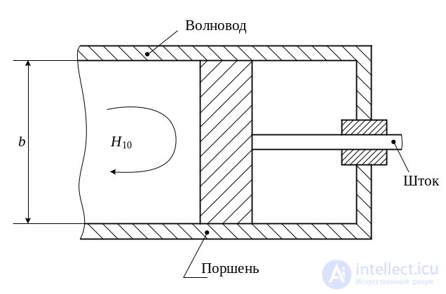
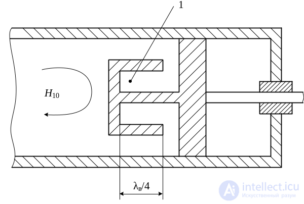
Fig. 3.2 Waveguide short-circuiting plungers:
a – contact type, b – choke type
An ideal reactive load has |Γ| = 1 and is characterized only by the phase of the reflection coefficient. A real reactive load has |Γ| close to unity, and is characterized by the coefficient ksw, which can reach values on the order of 100 or more. In practice, a reactive load is implemented as a fixed (sealed) or movable plunger. The main requirement for the plunger is to ensure good electrical contact with the walls of the transmission line. Fig. 3.2 shows waveguide short-circuiting plungers – contact type and choke type. In the choke plunger, contact quality is ensured electrically. The choke is a folded short-circuited half-wave line that transforms zero impedance into the cross-section of the waveguide adjoining the plunger. The mechanical contact is located at a distance of λg/4 from the short circuit (point 1 in Fig. 3.2, b). Therefore, there are no longitudinal currents in the mechanical contact cross-section, and the quality of this contact does not affect the overall performance of the plunger. Plungers in coaxial design are made similarly. They are used in microwave measuring paths, as well as tuning elements in matching devices.
Microwave power dividers are used in microwave transmission paths to distribute the power of microwave sources – oscillations among several channels in the required ratio. The following types of microwave power dividers are distinguished: T-junctions; directional couplers; bridge devices; multichannel microwave power dividers.
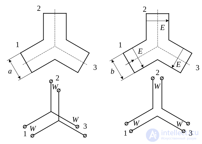
T-junctions. A T-junction is a joint of three transmission lines. T-junctions are represented on the equivalent circuit as a six-terminal network. Fig. 3.3, a) and b) show symmetric waveguide Y-junctions in the H and E planes respectively, along with their equivalent circuits. Let us determine the scattering matrices of these devices.
a) b)
Fig. 3.3 Symmetric waveguide Y-junctions and their equivalent circuits: a – in the H plane,
b – in the E plane
The scattering matrix of a six-terminal network is of third order (corresponding to the number of terminal pairs of the multiport network, or inputs of the microwave device). The reflection coefficient s11 is determined by connecting a generator to input 1, and matched loads to the rest. In this case, the load of the equivalent line corresponding to input 1 is the parallel connection of two lines with characteristic impedance W, equivalent to inputs 2 and 3, i.e., Zl = W/2. s11 = (Zl – W)/(Zl + W) = – 1/3. For the same reason, the transmission coefficients from input 1 to inputs 2 and 3 are equal, i.e., s21 = s31. Since we are considering an ideal lossless Y-junction, its scattering matrix is unitary. Therefore, the sum of the squared moduli of the elements of any row or column of this matrix equals unity, i.e., | s11|2 + | s21|2 + | s31|2 = 1. Given this, we find | s21| = | s31| = 2/3. The terminal planes of this device can be positioned so that all elements of the first column of the scattering matrix become real. Given that the Y-junction is a reciprocal device and its scattering matrix is symmetric, we obtain:
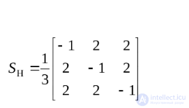 . (3.1)
Reasoning similarly for the symmetric Y-junction in the E plane, we obtain:
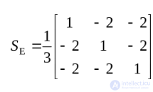 . (3.2)
The "minus" sign in the transmission coefficients of this matrix is explained by the fact that when, for example, input 1 of the Y-junction is excited, the orientation of the E vector at the remaining inputs is reversed (see Fig. 3.3, b). Y-junctions can be analyzed taking into account their geometric symmetry about the axis and the plane passing through the middle of each waveguide. Using the method for the effect of geometric symmetry of microwave devices on their external characteristics, one can obtain scattering matrices for such devices that coincide with (3.1) and (3.2).
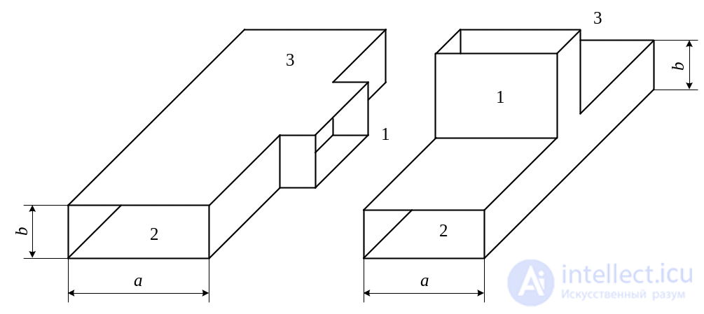
a) b)
Fig. 3.4 Waveguide T-junctions:
a – in the H plane, b – in the E plane
Fig. 3.4, a) and b) show waveguide T-junctions in the H and E planes respectively. They are usually made so that they are matched at input 1. Therefore, when these inputs are excited, the power is divided equally between arms 2 and 3 (the inputs of a microwave device are sometimes called arms). Hence 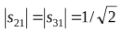 . In the H-junction, arms 2 and 3 are excited in phase, while in the E-junction – in antiphase. Given this and the unitarity property of the matrix ( ), we obtain the following scattering matrices for T-junctions:
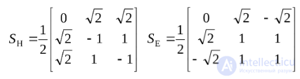 (3.3)
(3.3)
Fig. 3.5, a) and b) show junctions in coaxial and stripline designs respectively. They have scattering matrices the same as the waveguide H-junction.
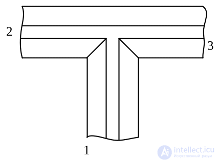
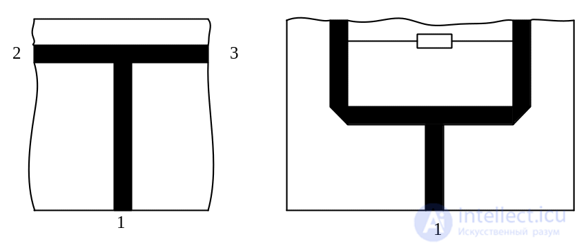
a) b)
Fig. 3.5 Junctions: a – coaxial, b – stripline
Fig. 3.6 Balanced stripline power divider
In practice, the task of combining the power of two sources into a common load is often encountered. Let us consider the possibility of using, for example, a T-shaped H-junction for this purpose. Connect the first source with amplitude a1 to arm 2 of the junction, the second source with amplitude a2 to arm 3, and a matched load to arm 1. Let us find the amplitudes of the waves bn (n = 1, 2, 3) reflected from the junction using the determinant of the scattering matrix:
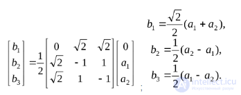
It follows that the power of the sources adds in arm 1 of the junction only when a1 = a2. Otherwise, undesired reflected waves appear in arms 2 and 3 of the junction. To eliminate these waves at any source amplitudes, the scattering matrix of the six-port power-combining device must have the form:
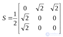 .
.
Since this matrix is symmetric, it corresponds to a reciprocal device. Let us determine whether there are thermal losses in this device. To do this, we find the eigenvalues of the scattering matrix as roots of the characteristic polynomial det(S – λSE) = 0. Substituting the matrix S here, we obtain: 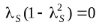 , from which λS1 = 0, λS2 = 1, λS3 = –1. Thus, when the microwave device is excited by the first eigenvector of matrix S, it must be completely absorbed by this device, while the second and third eigenvectors must be completely reflected from the microwave device. These properties are possessed by the matched junction (or balanced power divider), the stripline version of which is shown in Fig. 3.6. It includes an absorbing element in the form of a resistor R, whose resistance value, as well as the characteristic impedances of the arms, are selected to ensure the maximum operating frequency band of the device.
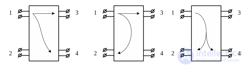
Directional couplers. Directional couplers are reciprocal microwave devices with four arms. When one of the arms is excited, the power is divided in the required ratio between two of the arms, while the fourth arm remains unexcited. On the equivalent circuit, a directional coupler is represented as an eight-port network. Depending on the arrangement of the inputs of the directional coupler between which the microwave power is divided, they are classified into three types, shown in Fig. 3.7. The first type (I) is called co-directional, the second (II) and third (III) – contra-directional.
I II III
Fig. 3.7 Eight-port networks equivalent to directional couplers of types I, II, and III
From Fig. 3.7 it follows that by renumbering the inputs of directional couplers of types II and III, they can be reduced to type I. Therefore, we will further consider directional couplers of type I. Ideal directional couplers have a scattering matrix of the form:
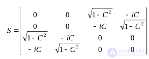 , (3.4)
where C is the coupling coefficient, which determines the fraction of coupled power. From the form of matrix S it follows that all inputs of the directional coupler are matched (s11= s22 = s33 = s44 = 0), inputs 1 and 2, as well as 3 and 4, are mutually isolated, i.e., s21 = s12 =0 and s43 = s34 = 0.
When arm 1 is excited, the phase of the oscillations in arm 4 lags by 90° behind the phase of the oscillations in arm 3. This is indicated by the negative imaginary unit in the coefficient C. Real directional couplers are characterized by the following parameters, determined in the mode where arm 1 is excited: the coupling loss c41 = 10 lg(P1/P4) = –20 lgC; the directivity c24 = 10 lg(P4/P2); the operating attenuation c31 = 10 lg(P1/P3); the standing wave ratio (SWR) at the input, equal to (1 + |s11|)/(1 – |s11|). These parameters are determined over a certain frequency band of the directional coupler, and their numerical values lie within 0 ≤ c41 < 60 dB; c24 > 20 dB; c31 > dB; ksw ≈1.1.
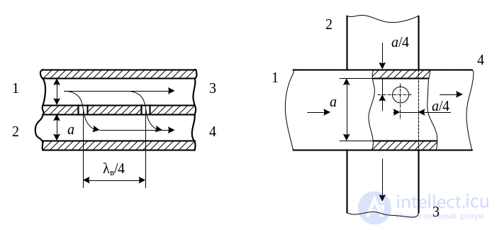
Fig. 3.8 Two-hole directional coupler
Fig. 3.9 Directional coupler on crossed waveguides
The simplest directional coupler is the waveguide two-hole coupler (Fig. 3.8). It consists of two rectangular waveguides, in whose common narrow wall two coupling holes are cut at a distance of λg/4 from each other. When arm 1 is excited, the microwave power mainly passes to arm 3, and a small portion of it is coupled to arm 4. Arm 2 remains isolated, since the waves coupled through the holes, spaced λg/4 apart, turn out to be in antiphase in this arm and cancel each other out. The disadvantage of this device is its narrow bandwidth. To eliminate this drawback, the directional coupler is made multi-hole. This also makes it possible to select the required frequency response of the coupling loss c41.
In waveguide microwave paths, a directional coupler is widely used consisting of two rectangular waveguides crossing at a right angle, in whose common broad wall a coupling hole of some shape is cut at a distance of a/4 from the narrow walls (Fig. 3.9). Possible shapes of the holes used in such couplers are shown in Fig. 3.10. The shape and size of the holes significantly affect the coupling loss value. In directional couplers with resonant-type elements (slots, cross-shaped holes), small coupling loss values can be achieved. The operating principle of such a hole is based on the fact that the hole location is a point of circular polarization of the magnetic field vector of the H10 wave. The direction of rotation of the H vector uniquely determines the direction of propagation of the H10 wave in the waveguide. Directional power coupling is explained by the conservation of the direction of rotation of the H vector in the upper and lower waveguides. To reduce coupling loss in such holes, two diagonally arranged cross-shaped coupling holes are made.
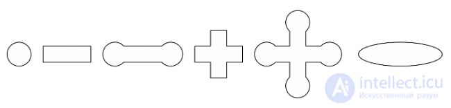
Fig. 3.10 Shapes of coupling holes used in directional couplers
a) b)
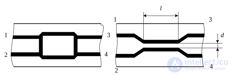
Fig. 3.11 Stripline directional couplers:
a – two-stub, b – on coupled lines
Fig. 3.11 shows stripline directional couplers. The two-stub coupler (Fig. 3.11, a) is an analog of the two-hole waveguide coupler. Stubs of length λl/4 play the role of the holes and are located at a distance of λl/4 from each other. The required coupling loss and input matching are ensured by selecting the characteristic impedances of the stubs and the line connecting them. The operating principle of the stripline coupler on coupled lines (Fig. 3.11, b) is that directional coupling from the main line (1 – 3) to the secondary line (2 – 4) is achieved through positioning it within the field of line (1 – 3). For this, the distance d between the lines is made sufficiently small. The coupling loss value in such a coupler depends on the gap between the lines d and on the length of the coupled section l. In such a directional coupler, coupling distributed along the length is ensured between the lines.
Microwave bridge devices. Microwave bridges are directional couplers with a coupling loss of 3 dB. Thus, the bridge divides the power equally between arms 3 and 4 (see Fig. 3.7).
a) b)
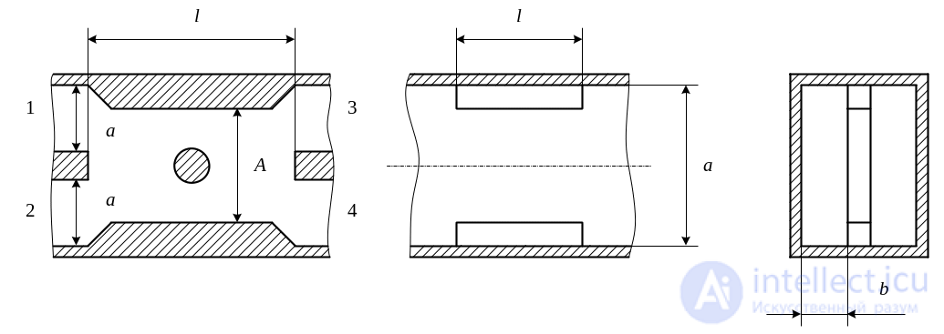
Fig. 3.12 Waveguide-slot bridges:
a – in the H plane, b – in the E plane
The following microwave bridge devices are distinguished: waveguide-slot bridges in the H and E planes; ring bridge; double T-bridge; folded double T-bridge. Microwave bridges, being a special case of directional couplers, are represented on the equivalent circuit as an eight-port network.
The waveguide-slot bridge in the H plane (Fig. 3.12, a) consists of two rectangular waveguides, where a section of length l of their common narrow wall is often cut out. This results in a wide rectangular waveguide with cross-sectional dimensions A × b. The dimension A of this waveguide is chosen such that the waves H10 and H20 propagate in it, i.e., λ < A < 3λ/2. When arm 1 is excited by the H10 wave, the waves H10 and H20 are excited in the wide waveguide. The diagrams of the transverse components of the electric field of these waves at the excitation point are shown in Fig. 3.13. From the graphs it follows that in the region of input 2 of the bridge a ≤ x ≤ 2a, the waves H10 and H20 of the wide waveguide are in antiphase. Therefore, arm 2 is isolated. The waves H10 and H20 in the wide waveguide have different phase velocities. Therefore, at the location of arms 3 and 4 they acquire a phase difference  , where
 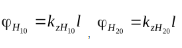 . Here ;

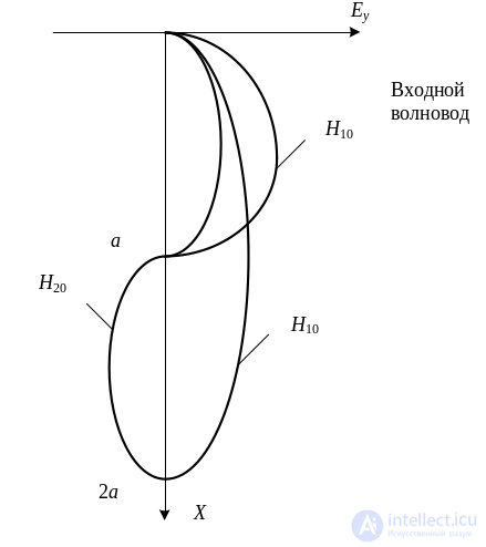
Fig. 3.13 Electric field diagrams of waves H10 and H20 in the plane of inputs 1 and 2 of the waveguide-slot bridge
– longitudinal propagation constants of the waves H10 and H20 in the wide waveguide. For the power to be divided equally between arms 3 and 4, the length l must be chosen such that  . Thus, the minimum bridge length is determined from the condition
The waveguide-slot bridge in the Е-plane operates similarly (Fig. 3.12, b). It consists of two rectangular waveguides in whose common broad wall two rectangular apertures are cut, adjoining the narrow walls. Thus, over a section of length l a rectangular coaxial line is formed. In the region of the coupling apertures, Т and Н10 waves are excited. The bridge length l is chosen from the condition that the phase difference between these waves equals π/2: 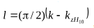 , where k = 2π/λ.
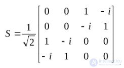
Waveguide-slot bridges in the Н- and Е-planes have identical scattering matrices:
 .
.
A ring bridge is a transmission line of length 3λg/2 folded into a ring, into which four input transmission lines are connected at intervals of λg/4. Rectangular waveguide in the Е- and Н-planes, coaxial line, stripline, and similar lines can be used as the transmission line. As an example, Fig. 3.14 shows a ring bridge implemented in stripline.
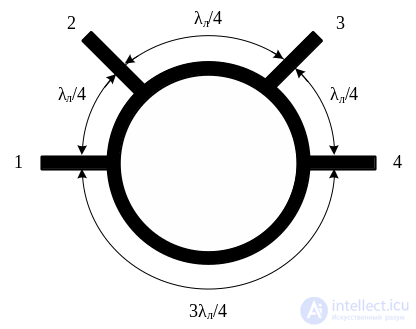
Fig. 3.14 Stripline ring bridge
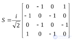
When arm 1 is excited, waves propagate around the ring in both directions; these waves turn out to be in phase in the region of arms 2 and 4, and out of phase in the region of arm 3. Therefore, power is divided equally between arms 2 and 4, while arm 3 is isolated. Here arms 2 and 4 are excited in antiphase, since the distance between them equals λg/2. Matching of the bridge inputs is achieved by selecting the wave impedances of the line and of the ring line. Exciting each arm of the ring bridge in turn, one can construct the scattering matrix:
 .
.
The double Т-bridge is another representative of waveguide bridge devices (Fig. 3.15). It is a hybrid of waveguide Е- and Н-tees. (see Fig. 3.4). When arm 1 is excited, power is divided equally between arms 3 and 4, exciting them in phase. Arm 2 turns out to be isolated, because the electric field vector of the Н10 wave of arm 1 is oriented along the waveguide of arm 2, exciting Е-type waves in it that are in a cutoff (evanescent) regime. When arm 2 is excited, power is likewise divided equally between arms 3 and 4, but exciting them in antiphase. Arm 1 turns out to be isolated, since the electric field vector of the Н10 wave of arm 2 is oriented parallel to the broad walls of the waveguide of arm 1, exciting H0n (n = 1, 2, …) type waves in it, which are in a cutoff regime. Taking into account the reciprocity of this device, the scattering matrix can be written as:
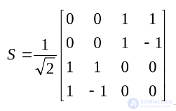 .
.
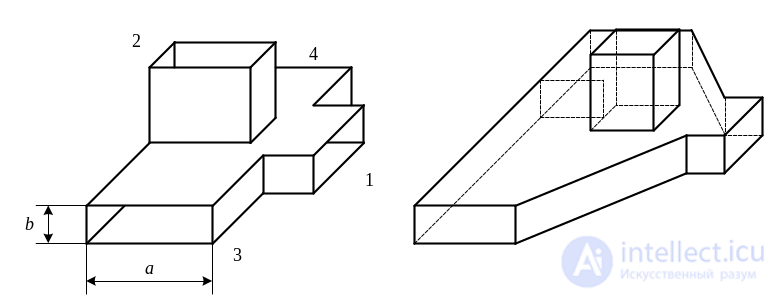
Fig. 3.16 Folded double Т-bridge Fig. 3.15 Double Т-bridge
A distinctive feature of the double Т-bridge is that it sums the powers of in-phase, equal-amplitude sources connected to arms 3 and 4 in arm 1, and of out-of-phase sources in arm 2. For this reason, such devices are used in monopulse radar antennas to form sum-difference patterns.
The folded double Т-bridge (Fig. 3.16) is a variant of the double Т-bridge and has the same scattering matrix.
Multichannel microwave power dividers. Such power dividers are used in the feed networks of multielement antenna arrays (AAs). They are designed to divide the power of a source in a required ratio among a large number of output channels exciting the radiating elements of the AA. An equivalent multiport network of such a divider is shown in Fig. 3.17.
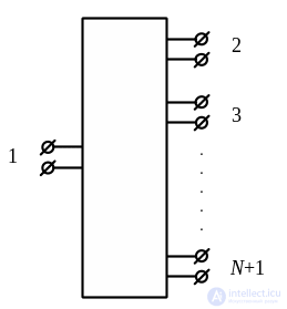
Fig. 3.17 Multichannel microwave power divider
The power of the source connected to the first pair of terminals (the input) must be distributed among N output pairs of terminals. Tees, balanced power dividers, bridge devices, and their combinations can serve as elements for building such dividers. The most common schemes for constructing multichannel dividers are the parallel (Fig. 3.18, а), series (Fig. 3.18, б), and series-parallel (Fig. 3.18, в) configurations. Each small square in these diagrams denotes an elementary power divider.
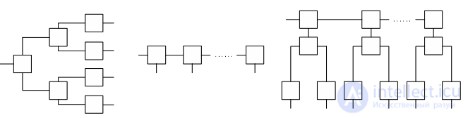
Fig. 3.18 Diagram of multichannel power dividers:
а – parallel, б – series,
в – series-parallel
The characteristics of multichannel dividers can be found from the known characteristics of the elementary dividers by combining them into an overall circuit using the method described in Section 2.1. Questions of the calculation and design of such power dividers are treated in the monograph by N.T. Bov, Microwave Microelectronic Devices (Kiev: Tekhnika, 1984).
Microwave control devices are intended to change the amplitude, phase, or polarization in a microwave path. The parameters of the oscillations in the path can be changed by mechanical displacement of its elements. Such control devices are called mechanical. The parameters of the oscillations can also be changed by altering the medium filling the elements of the path under the action of electrical signals. Such control devices are called electrical. A medium with electrically controllable parameters can be implemented in the form of microwave semiconductor diodes, magnetized ferrites and ionized plasma, or ferroelectrics. There are also electromechanical control devices, in which mechanical displacements of the elements of the path occur under the action of electrical signals, changing the parameters of the microwave oscillations. Such devices are built, for example, on the basis of piezoelectric elements.
Control devices that change the amplitude of microwave oscillations include switches, commutators, attenuators, and power limiters. Control devices that change the phase of microwave oscillations include phase shifters. Devices that change the plane of polarization of a passing wave are called polarizers.
Devices for controlling the amplitude of microwave oscillations. The simplest device for controlling the amplitude of microwave oscillations is a microwave switch, which is represented in the equivalent circuit as a two-port network. It has two modes of operation: a transmission mode, in which microwave power passes freely from input to output, and a blocking mode, in which microwave power does not reach the output because of absorption in the switch or reflection from it. A mechanical implementation of such a device amounts to simply blocking the cross-section of the microwave transmission line with a reflecting shutter or an absorbing load. Such shutter-type waveguide switches are used in radar stations to protect the receiver input circuits from interference created by nearby closely spaced stations. They have a switching speed of 10-5 s. At present, semiconductor switches are most often used in the microwave range. Their basis is a microwave semiconductor diode, which can have a p-n, p-i-n, or n-i-p-i-n structure.
p-n type diodes have a switching time on the order of 10-7…10-8 s. Varactor diodes with a p-n junction, made from single crystals of silicon, germanium, or gallium arsenide, have the highest speed (10-10 s), but can handle microwave power only in hundredths of a watt.
p-i-n type diodes have a speed of 10-7…10-6 s at pulse powers of hundreds of kilowatts.
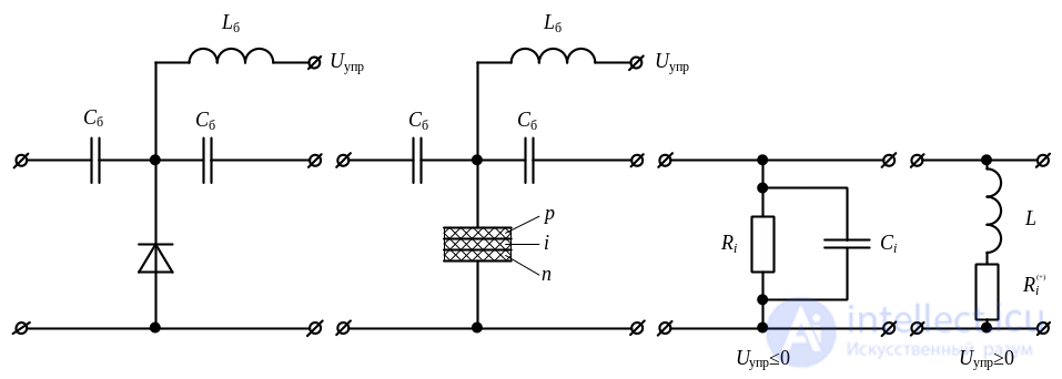
n-i-p-i-n type diodes are essentially a dual p-i-n diode. Structurally, microwave diodes are made without a case, with a maximum size of 1 mm; without a case but with a metal heat sink; in a metal case; and also in combination with a resonant waveguide iris. In waveguides, diodes are usually connected in parallel (Fig. 3.19, а, б, where Cb, Lb are the high-frequency blocking elements of the diode supply circuit; Uctrl is the control voltage on the diode; L is the inductance of the diode leads; Ri is the base resistance of the diode; Ci is the base capacitance of the diode).
а) б) в) г)
Fig. 3.19 Connection of a p-i-n diode into a waveguide and its equivalent circuits
The base of the diode is the name given to the high-resistivity i-region with intrinsic-type conductivity. At zero or negative voltage Uctrl, the diode has high resistance (tens of kilohms). Its equivalent circuit is shown in Fig. 3.19, в). In this case the capacitance Ci is 0.3…1 pF. At Uctrl > 0 (~ 1…2 V) the base of the diode becomes saturated with electrons and holes, its resistance decreases sharply, and the value  (Fig. 3.19, г) is on the order of a few ohms. In this case, the current consumed by the diode is 100 mA. In this mode the diode is capable of passing microwave currents up to 100 A.
Fig. 3.20 shows the design of the simplest waveguide switch in the form of a resonant iris with an n-i-p-i-n diode.
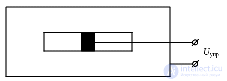
Fig. 3.20 Resonant iris with an n-i-p-i-n diode
Applying a voltage Uctrl > 0 to the diode corresponds to the blocking mode of the switch, since the low resistance of the diode shunts the parallel resonant circuit of the resonant iris. When the diode is directly incorporated into the iris, its resonant frequency shifts because of the diode capacitance Ci, which is compensated by shortening the slot of the iris.
The main characteristic of a semiconductor microwave switch is its quality factor К, defined as the ratio of the diode's active resistances in the closed and open states, and equal to 103 ÷ 104. The quality factor determines the attenuation of microwave power in the switch in the blocking and transmission modes. It can be said that a switch that is optimal by the criterion of maximum controllable power introduces an attenuation in the blocking mode of  and in the transmission mode of
 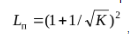 , which corresponds to Lbl = 30.3 dB at К = 103 and Ltr = 0.27 dB.
Microwave commutators are devices designed to transfer microwave power from one or several inputs to one or several switchable outputs; in the equivalent circuit they are represented as a multiport network. When transferring microwave power from an input to an output of the commutator, the losses must be minimal. Fig. 3.21 shows a mechanical rotary commutator.
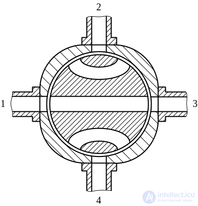
Fig. 3.21 Mechanical waveguide commutator
Switching of the inputs in it is achieved by a simple rotation of the rotor through an angle that is a multiple of π/2. Electrically controlled multichannel commutators can be built on the basis of microwave semiconductor switches and power dividers, such as bridges.
Microwave attenuators are designed for smooth or discrete reduction of the amplitude of microwave oscillations. In the equivalent circuit they are represented as a two-port network. The reduction of amplitude in an attenuator may be caused by thermal losses or by reflections from it.
The simplest smooth mechanical attenuator is a section of rectangular waveguide with a slot cut along the axis in the broad wall, through which a plate coated with a radio-absorbing material is inserted into the waveguide. The plate has a convex profile, and the deeper it is inserted into the waveguide, the greater the attenuation it introduces. The amount of attenuation L is defined as the ratio of the power Рin at the input of the attenuator to the power at the output Рout and is measured in decibels: 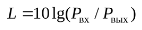 . A section of below-cutoff waveguide, in which the amplitude of the oscillations decreases exponentially, can serve as an attenuator with fixed attenuation.
Discrete attenuators can be built as cascaded sections, each consisting of a Т-junction, a diode switch, and a matched load. Each section introduces a fixed attenuation. From section to section, the amount of attenuation introduced changes according to a binary law. For example, an attenuator consisting of cascaded sections with attenuations of 1, 2, 4, 8, and 32 dB can introduce attenuation up to 63 dB in steps of 1 dB.
Microwave power limiters are designed to pass low-amplitude microwave oscillations from input to output without attenuation, while limiting the amplitude of oscillations that exceed a specified threshold value. In the equivalent circuit they are always depicted as a nonlinear two-port network whose characteristics depend on the amount of power applied. Typical representatives of the devices under consideration are microwave antenna switches (duplexers). They make it possible to use the same radar antenna both for transmitting powerful pulses and for receiving weak signals reflected from targets. During the radiation of powerful pulses it is necessary to disconnect the receiver from the path, while in the intervals between pulses the transmitter is disconnected from the antenna and the receiver is connected.
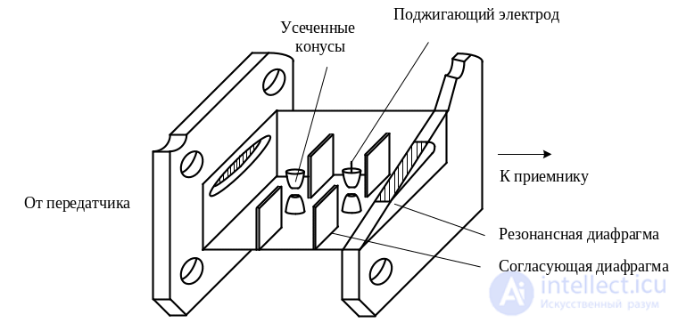
Fig. 3.22 Receiver protector discharge tube
In practice, a gas discharge tube, which is a waveguide electrovacuum device, is most often used as the antenna switch (Fig. 3.22). It is a section of rectangular waveguide of length 3λg/4, whose inputs are closed by resonant irises hermetically sealed with a high-quality dielectric. Between the resonant irises, at a distance of λg/4 from each other on the axis of the waveguide, are two pairs of cone-shaped electrodes, which in the absence of a discharge are equivalent to a capacitance. To match these capacitances, inductive irises are also included here, which together with them form resonant circuits. Thus, in the absence of a discharge, the device is a bandpass filter consisting of four coupled resonant circuits with a passband of 5÷10%. A discharge between the electrodes arises automatically during the passage of a powerful pulse. The firing threshold of the discharge tube is set by an igniter electrode, which is connected to a DC source that maintains a glow discharge in this electrode. The glow discharge is maintained by partial ionization of the gas filling the discharge tube. When a powerful microwave pulse arrives from the input side, a discharge occurs at the igniter electrode. After this, the second pair of electrodes, located at the maximum of the electric field, breaks down. Then breakdown of the input resonant iris occurs, disconnecting the receiver from the antenna. The main characteristics of such discharge tubes are the arc losses, the firing time, and the recovery time. A correctly designed discharge tube should introduce low losses both during reception and during transmission of signals. The firing time of the discharge tube is 10-8 s, and the recovery time is 10-6 s. Such devices are installed directly at the input of the receiver and are called receiver-protector discharge tubes. They have a low firing threshold owing to the use of an igniter electrode. Transmitter-blocking discharge tubes are also used in the paths of radar stations; their firing threshold is significantly higher than that of receiver-protector discharge tubes because they lack an igniter electrode. Fig. 3.23 shows the balanced circuit of such an antenna switch.
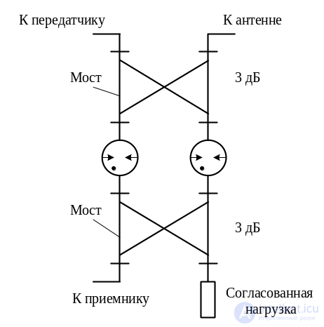
Fig. 3.23 Diagram of a balanced antenna switch
When the transmitter is operating, microwave power is divided equally between the discharge tubes by means of a bridge and fires them. Reflected from the discharge tubes, the microwave power passes through the same bridge into the antenna. A small portion of the power that passes through the discharge tubes passes through the second bridge into a matched load. In the interval between pulses, microwave oscillations received by the antenna, having passed through the first bridge, the unfired discharge tubes, and the second bridge, pass to the input of the receiver. To improve the quality of operation of such a switch, identity of the characteristics of the discharge tubes included in it is required.
Microwave phase shifters. Microwave phase shifters are designed to change the phase of a reflected or transmitted wave by a required amount. Various designs of such devices are widely used in microwave paths, especially in the paths of phased antenna arrays. Reflective and transmission-type microwave phase shifters are distinguished. Reflective phase shifters are represented in the equivalent circuit as one-port networks, and transmission-type ones as two-port networks. There are mechanical, electrical, and electromechanical phase shifters. Phase shifters with smooth and discrete phase changes are also distinguished.
The simplest reflective mechanical phase shifter is a section of transmission line with a short-circuiting plunger. Such a device is characterized by a scattering matrix that degenerates into a single number – the reflection coefficient at the input of the phase shifter. As the position of the plunger in the line changes, the phase of the reflection coefficient also changes.
A discrete reflective phase shifter is built on the basis of semiconductor switches. A waveguide version of such a phase shifter is shown in Fig. 3.24, where 1 – rectangular waveguide; 2 – diaphragm; 3 – n-i-p-i-n-diode.
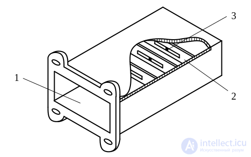
Fig. 3.24 Reflective phase shifter
The distance l between the diaphragms is chosen depending on the required discrete phase step Δφ:
Δφ = – 2kzl,
where kz – the longitudinal propagation constant of the wave in the waveguide. The presence of the factor of two is due to the wave traveling the distance l twice. For example, l = λg/8 at Δφ = – π/2.
The simplest transmission-type phase shifter is a section of transmission line of length l, which has a scattering matrix of the form:
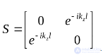 .
.
The inputs of the phase shifter are matched, i.e., the diagonal elements of its scattering matrix are equal to zero. The losses introduced by such phase shifters are minimal, i.e., the modulus of the transmission coefficients of the scattering matrix is equal to unity. The magnitude of the phase shift introduced by the simplest phase shifter is determined by the relation:
φ = – kzl.
It follows that φ depends on the line length l and the propagation constant kz. By changing one of these quantities, the phase φ can be changed. The general expression for kz has the form:
 .
.
It can be seen that the value of kz can be changed by changing the parameters ε or μ of the medium filling the transmission line, or by changing the cross-sectional dimensions of the line, which changes λcr.
The simplest mechanical transmission-type phase shifter with variable length is the trombone phase shifter, shown in Fig. 3.25.
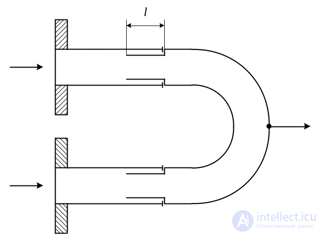
Fig. 3.25 Waveguide trombone phase shifter
Waveguide coaxial phase shifters are built on this principle. The maximum value of the introduced phase shift is determined by the value 2Δl – twice the travel of the movable part of the phase shifter.
Fig. 3.26 shows a mechanical transmission-type waveguide phase shifter in which the phase changes due to the transverse movement of a dielectric plate in the waveguide. If the plate is pressed against the narrow wall of the waveguide, where the intensity of the transverse field components is low, then the phase velocity of the wave in the waveguide changes insignificantly compared to the empty waveguide. As the plate is moved toward the middle of the waveguide, the intensity of the transverse field components increases, the phase velocity of the wave in the waveguide decreases, and therefore the phase shift introduced by the dielectric plate increases.
Fig. 3.27 shows a mechanical squeeze-type transmission waveguide phase shifter. It consists of a rectangular waveguide carrying the H10 wave, along the axis of whose broad walls long radiating slots are cut. When such a waveguide is squeezed from the narrow walls, its dimension a decreases, therefore λcr = 2a changes, and, consequently, so does the phase velocity of the wave in the waveguide 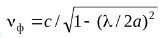 .
.
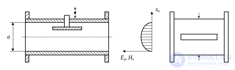
Fig. 3.26 Mechanical phase shifter
Fig. 3.27 Mechanical squeeze-type phase shifter with a movable dielectric plate
This leads to a change in the magnitude of the phase shift introduced by such a phase shifter.
Mechanical phase shifters are used in laboratory and measurement setups. They have low speed, i.e., a low rate of phase change.
Fig. 3.28 shows a transmission-type waveguide ferrite phase shifter. It consists of a section of rectangular waveguide, inside which a longitudinally magnetized ferrite rod is placed.
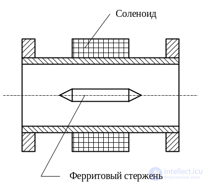
Fig. 3.28 Reciprocal ferrite phase shifter
The longitudinal magnetic field in the rod is created by a solenoid wound directly on the waveguide. The magnitude of the phase shift of such a phase shifter depends on the magnitude of the magnetizing field, which is determined by the magnitude of the current flowing through the solenoid. When the current in the solenoid changes, the magnetizing field also changes, which leads to a change in the magnetic permeability of the rod and, consequently, the phase velocity of the passing wave.
Phase shifters with continuous phase variation are called analog. A drawback of the analog ferrite phase shifter is the low accuracy of phase setting and the need for a continuous control current to flow through the solenoid in order to maintain the required phase shift.
Discrete phase shifters have become the most widespread in practice; compared to continuous phase shifters, they have high speed, greater accuracy of phase setting, and greater repeatability of characteristics in mass production. A waveguide version of a discrete semiconductor phase shifter with a phase step of Δφ = – π/2 is shown in Fig. 3.29. It consists of an H-plane waveguide slot bridge, into two adjacent arms of which reflective phase shifters are connected (see Fig. 3.24), each having three semiconductor switches.
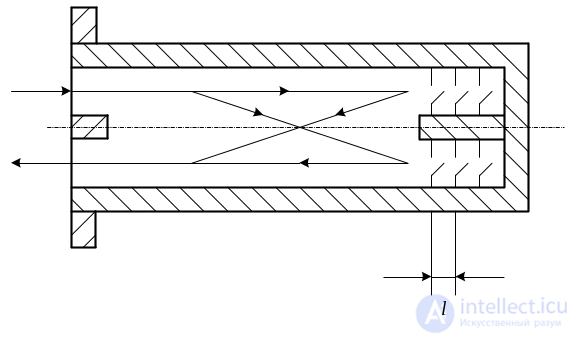
Fig. 3.29 Transmission-type waveguide phase shifter
Microwave oscillations fed to one of the inputs of such a phase shifter, after passing through the bridge and reflecting from the semiconductor switches in the blocking state, pass through the bridge a second time and reach the output of the phase shifter. The magnitude of the introduced phase shift depends on the number of the closed switch of the upper and lower reflective phase shifters, operating synchronously, and on the distance l between the switches. A stripline transmission-type switched phase shifter based on a square bridge can be implemented similarly.
Fig. 3.30, a) shows a discrete ferrite phase shifter with Δφ = – π/4. It consists of a rectangular waveguide, inside which three toroidal ferrite elements are placed, having a «rectangular» hysteresis loop (RHL), shown in Fig. 3.30, b). The ferrite is magnetized by current pulses flowing through wires passing through the toroids. The amplitude of the control pulses Ictrl is chosen so that the ferrite reaches saturation in terms of magnetic induction B. The value of the phase shift introduced by one ferrite toroid is determined by the magnitude of the magnetic induction ±Br.
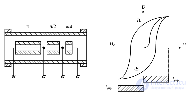
a) b)
Fig. 3.30 Non-reciprocal transmission-type phase shifter based on ferrite with RHL:
a – phase shifter design; b – hysteresis loop and control current pulses
The main advantage of such phase shifters is the presence of internal magnetic memory. This is manifested in the fact that ferrites with RHL retain their magnetization state indefinitely, and the control current flows only while the ferrite is being remagnetized. Moreover, the current pulses have a duration on the order of 10-6 s and an amplitude of 20…30 A. Such phase shifters are widely used in practice and operate in a frequency band of 5…10% of the center frequency, introducing additional heat losses of about 1 dB at an input kswr of about 1.2. The average power level of the microwave oscillations fed to the input of the phase shifter can reach 0.5 kW. It should be noted that the ferrite phase shifter under consideration is a non-reciprocal device, i.e., the magnitude of the introduced phase shift changes when the direction of wave propagation in the waveguide is reversed. Preserving the phase shift for a wave propagating in the opposite direction is achieved by reversing the direction of the control current in the wires. The non-reciprocity of the phase shifter is explained by the fact that a ferrite magnetized transversely with respect to the propagation of the microwave wave has different values of magnetic permeability for waves with opposite directions of rotation of the magnetic field vector. The sections of the ferrite toroids parallel to the narrow walls of the waveguide are located in regions where the magnetic field vector of the H10 wave, at each fixed point, rotates parallel to the broad wall of the waveguide. The direction of rotation is set by the direction of wave propagation. When the direction of wave propagation in the waveguide changes, the direction of rotation of the vector H of this wave relative to the direction of the magnetizing field H0 changes (Fig. 3.31). Therefore, the magnetic permeability of the ferrite and the magnitude of the introduced phase shift change.
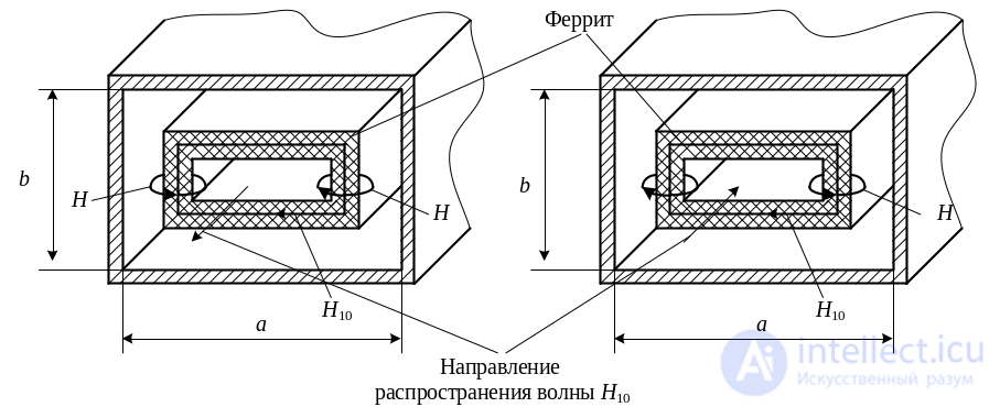
Fig. 3.31 Cross-sections of the phase shifter based on ferrite with RHL
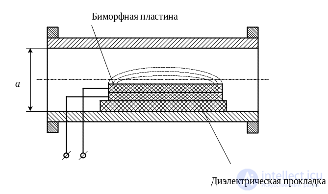
a – phase shifter design;
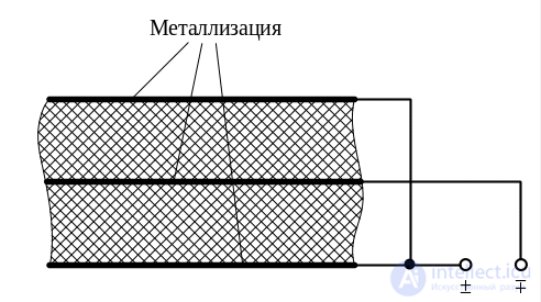
b – cross-section of the bimorph plate
Fig. 3.32 Electromechanical strictive phase shifter:
An example of an electromechanical phase shifter is shown in Fig. 3.32, a). Its operating principle is based on the use of the electrostriction effect, which consists in the deformation of certain dielectric materials, called piezoelectrics, under the action of an applied electric voltage. This effect is most strongly expressed in dielectric samples made from lead zirconate titanate ceramics. Thin plates are made from this ceramic and glued together with like-polarity sides facing each other (Fig. 3.32, b). Such two-layer plates are called bimorph plates. Under the action of an electric voltage applied to the metallized sides of the bimorph plate, it bends in a direction determined by the polarity of the applied voltage. The magnitude of the deflection depends on the magnitude of the applied voltage. In the electromechanical phase shifter shown in Fig. 3.32, a), the deflection of the bimorph plate leads to a reduction in the size of the broad wall of the rectangular waveguide. Due to the change in wave velocity in the region where the bimorph plate is located, the phase of the transmitted wave changes. Such and similar phase shifters are used in the millimeter wave band. The voltage applied to the bimorph plate is approximately hundreds of volts.
Microwave polarizers. Microwave polarizers are designed to change the polarization of the wave passing through the transmission line. In the equivalent circuit, they are represented as an eight-terminal network having two pairs of input and output terminals. Each pair of terminals at the input or output of such an eight-terminal network corresponds to waves in the waveguide with orthogonal polarizations. Such devices are usually implemented in a circular waveguide or in a waveguide of square cross-section with the H10 and H01 waves. The simplest polarizer based on a circular waveguide is shown in Fig. 3.33, a).
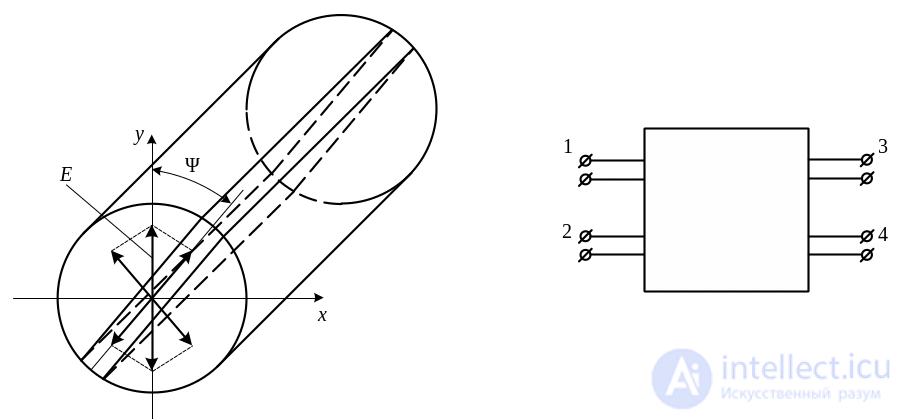
a) b)
Fig. 3.33 Polarizer based on a circular waveguide and its equivalent circuit
It is a section of circular waveguide of length l with a single propagating H11 wave, inside which a dielectric plate is placed at an angle Ψ to the vertical axis. Fig. 3.33, b) shows the equivalent eight-terminal network. Terminals 1 and 3 of this multiport correspond to the H11 wave of the circular waveguide, whose E vector, passing through the center of the cross-sectional circle, is perpendicular to the plate. Let us call this wave the perpendicular-polarization wave. Terminals 2 and 4 correspond to the H11 wave whose E vector is parallel to the plate. Let us call this wave the parallel-polarization wave. The presence of the dielectric plate in the waveguide causes the phase velocities of the parallel  and perpendicular
  polarization waves
  to differ. Therefore, the magnitudes of the phase shifts introduced by this plate for the parallel- and perpendicular-polarization waves turn out to be different. In this case, the phase difference
 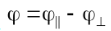 is determined by the length of the plate and the dimensions of its cross-section. Setting, for simplicity,
продолжение следует...
Часть 1 3. Elements of the Microwave Path, Microwave Loads, Microwave Power Dividers
Часть 2 3.4 Microwave devices using ferrites - 3. Elements of the

Comments