
Lecture
Semiconductors include materials with electron-hole conductivity whose resistivity at normal temperature lies between the resistivity values of conductors and dielectrics. The main feature of semiconductors is the significant dependence of their properties on various external factors: temperature, illumination, electric and magnetic fields, external pressure, etc. Unlike metals, semiconductors have a negative temperature coefficient of resistance over a wide temperature range. In the energy spectra of semiconductors there is a region of forbidden energies in which no electron states can exist. The allowed states form allowed energy bands above and below the forbidden-energy region. The uppermost of the allowed bands, completely filled with electrons at absolute zero, is called the valence band. It is followed by the forbidden band (band gap), and the next allowed band is the conduction band. It is empty at absolute zero and has conduction electrons (partially filled) at a temperature different from zero. A simplified energy diagram of a semiconductor is shown in Fig. 3.1. In an intrinsic semiconductor, the Fermi level EF lies in the middle of the forbidden band. EC is the bottom of the conduction band, EV is the top of the valence band, and the forbidden band lies between EC and EV. Unlike metals, where free electrons always exist, in semiconductors electrons must overcome the forbidden band and reach the conduction band in order to become free.
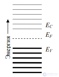
Fig. 3.1. Energy bands of an intrinsic semiconductor
The properties of semiconductors depend very strongly on the impurity content, even in small amounts. Not only the magnitude of the conductivity but also the character of its temperature dependence depends on the presence of impurities.
3.1. INTRINSIC AND EXTRINSIC SEMICONDUCTORS. MAJORITY AND MINORITY CHARGE CARRIERS
Intrinsic semiconductors are semiconductors in which the influence of impurities on the electrical conductivity at a given temperature can be neglected due to their small quantity. They contain no alloying (dopant) elements that are introduced during crystal growth to provide the required resistivity value.
At temperatures other than zero, some of the electrons, due to thermal fluctuations, overcome the potential barrier and end up in the conduction band. In an intrinsic semiconductor, when an electron transitions to the conduction band, a hole is formed in the valence band – a positive charge equal in magnitude to the charge of the electron. Thanks to the existence of holes, electrons of the valence band also take part in the conduction process by moving through the holes to higher allowed levels of the valence band. Thus, in this band the holes move opposite to the electrons, carrying a positive charge and possessing a certain effective mass.
The higher the temperature and the smaller the width of the forbidden band, the higher the rate of thermal generation of charge carriers – electrons and holes. Simultaneously with generation, the opposite process occurs in the semiconductor – recombination, i.e. the return of an electron to the valence band and the disappearance of a free electron-hole pair.
Extrinsic (doped) semiconductors, or alloyed semiconductors, are semiconductors containing donor or acceptor atoms, or stoichiometrically excess atoms, in a quantity comparable to the number of intrinsic charge carriers. The kinetic phenomena in semiconductors, including the magnitude and type of conductivity, as well as the optical properties of semiconductor materials, are significantly determined by the amount of impurities in semiconductors and the position of the impurity levels in the forbidden band.
Impurities in semiconductors are foreign atoms dissolved in semiconductors. Impurities in semiconductors either substitute for atoms of the base substance in the crystal lattice, forming substitutional solid solutions, or are located in interstitial positions, forming interstitial solid solutions.
A distinction should be made between residual impurities, which were not removed from the semiconductor during purification or were accidentally introduced into the semiconductor material during subsequent technological operations, and dopant (alloying) impurities, deliberately introduced in specified quantities into the semiconductor during doping, either during the preparation of the polycrystalline charge or the growth of a single crystal, or during the manufacture of p-n junctions, with the aim of imparting the required electrophysical properties to the entire material or to specific regions of it (for example, a certain magnitude and type of conductivity). The introduction of dopant impurities can provide reproducible results only if their concentration in the semiconductor (which must be below their solubility limit at temperatures close to room temperature) is significantly higher than the concentration of residual impurities. Depending on their effect on the physical properties of the semiconductor, impurities can be in an electrically active or electrically inactive state (depending on the conditions of introduction and processing). Electrically active impurities can be unambiguously active, i.e. behaving either as donors or as acceptors, or amphoterically active: some of the impurity atoms may exhibit donor properties, and others acceptor properties.
The electrical activity of an impurity is characterized mainly by the number and distribution of bonds of the impurity atom with neighboring atoms of the semiconductor. For example, in semiconductor crystals with a diamond-type structure (diamond, Si, Ge), the acceptors are elements of group III of the periodic table (whose atoms form bonds with only three of the four surrounding atoms and cause the appearance of a hole), while the donors are elements of group V (which, after forming bonds with all four neighboring atoms, have one free electron left over). The ionization energy of group III and V impurity atoms in Si and Ge is close to 0.01 eV, so at room temperature such impurities are almost completely ionized. At low concentrations, impurities create localized energy levels located in the forbidden band (impurity levels). Depending on whether the distance from the impurity level to the nearest allowed band is small compared to, or comparable to, the width of the forbidden band, a distinction is made between shallow and deep impurity levels. At high concentrations, the levels merge, forming impurity bands adjoining the allowed bands (such semiconductors are called heavily doped). In the manufacture of semiconductor devices, in order to create p-n junctions of the required configuration, it is sometimes necessary to locally overcompensate an impurity of one type (for example, an acceptor) with an impurity of another type (a donor) in order to create a layer of material of the required conductivity type.
The group of electrically inactive impurities (under certain conditions, for example at room temperature) includes atoms of those groups of the periodic table that are not unambiguous dopant impurities for a given semiconductor. These impurities create two (sometimes more) deep impurity levels in the forbidden band of the semiconductor. They are sometimes deliberately introduced into the semiconductor to impart special properties, for example a sharp reduction in the lifetime of minority charge carriers. Impurities of this type create deep levels, which are often effective centers for the capture and recombination of charge carriers. In some cases, for example in the manufacture of semiconductor crystallophosphors, doping with impurities that create deep levels is carried out, and the necessary radiative recombination occurs between the edge of one of the allowed bands and a deep level, or between two impurity levels, one of which is deep.
In semiconductor compounds of the AIIIBV or AIIBVI type, unambiguously active acceptors are atoms of elements with an oxidation state one less than that of component A or B, while donors are atoms of elements with an oxidation state one greater than A or B. For example, in GaAs, the acceptors are atoms of group II elements, and the donors are atoms of group VI elements; atoms of group IV elements are amphoterically active impurities: a Ge atom replacing a Ga atom is a donor, while one replacing an As atom is an acceptor.
In semiconductor compounds, the role of an impurity can be played by atoms of the components of the compound itself that are in excess relative to the stoichiometric composition, i.e. point defects.
In any semiconductor crystal purified to the practically achievable limit, there are always both residual impurities and thermally equilibrium (and non-equilibrium) point defects. Since all impurity atoms and point defects tend to ionize, complex interactions are established in semiconductors between all charged defects and charge carriers.
Breakdown in semiconductors is the phenomenon of a sharp increase in electric current through a semiconductor sample with a small change in the potential difference applied to the sample, leading to irreversible thermal destruction of the sample or a portion of it. The nature of such breakdown is related to the exponential growth in the semiconductor of the concentration of free charge carriers with increasing temperature: local heating of a region of the semiconductor is accompanied by an increase in the concentration of charge carriers and the local current density, which leads to a further rise in the temperature of that region, and so on.
Electrical conductivity of a semiconductor strongly depends on the concentration of charge carriers and is expressed by the relation:
σ = q(nµn + pµp),
where n and p are the concentrations of electrons and holes, respectively; µn and µp are the mobilities of electrons and holes, respectively.
The concentration of charge carriers is positively dependent on temperature. Consequently, the electrical conductivity of a semiconductor also depends on temperature. The temperature dependence of the electrical conductivity of a schematically doped semiconductor (not to scale) is shown in Fig. 3.2. Section I of the graph corresponds to the thermal generation of minority charge carriers from impurity atoms, since they are ionized at lower temperatures than the intrinsic atoms. In section II, all impurity atoms are ionized, while ionization of the intrinsic atoms has not yet begun, so there is no growth in conductivity. In section III, ionization of the intrinsic atoms of the semiconductor occurs and the concentration of majority charge carriers increases, which leads to a further increase in electrical conductivity.
As temperature increases, the mobility of the carriers also changes, decreasing as a result of increased scattering on thermal lattice vibrations. But the change in mobility is small compared to the change in carrier concentration, and therefore it plays practically no role in the change of electrical conductivity upon heating and cooling.
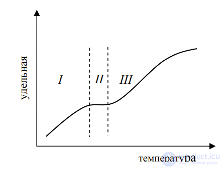
Fig. 3.2. Temperature dependence of the electrical conductivity of a doped semiconductor:
I – region of impurity conduction; II – absence of thermal generation;
III – impurity and intrinsic conduction

Comments