
Lecture
Radiation hardening is the process of designing electronic components and circuits that are resistant to damage or malfunction caused by high levels of ionizing radiation (particulate radiation and high-energy electromagnetic radiation), especially for environments in outer space (particularly beyond low Earth orbit), around nuclear reactors and particle accelerators, or during nuclear accidents or nuclear war.
Most semiconductor electronic components are susceptible to radiation damage, and radiation-hardened (rad-hard) components are based on their non-hardened equivalents with certain design and manufacturing changes that reduce susceptibility to radiation damage. Because of low demand and the extensive development and testing required to create a radiation-hardened microelectronic chip design, radiation-hardened chip technology tends to lag behind the latest developments. They are also usually more expensive than their commercial counterparts.
Radiation-resistant products are typically subjected to one or more tests to determine resulting effects, including total ionizing dose (TID), enhanced low dose rate effects (ELDRS), neutron and proton displacement damage, and single event effects (SEE).
Radiation-hardened integrated circuit — an integrated circuit subject to increased requirements for resistance to failures caused by exposure to radiation. The main application area for such circuits is spacecraft, military equipment and medical electronics.
Environments with high levels of ionizing radiation create special design challenges. A single charged particle can knock out thousands of electrons, causing electronic noise and signal spikes. In digital circuits this can lead to inaccurate or garbled results. This is a particularly serious problem when designing satellites, spacecraft, future quantum computers, military aircraft, nuclear power plants, and nuclear weapons. To ensure the proper operation of such systems, manufacturers of integrated circuits and sensors intended for the military or aerospace markets use various radiation hardening techniques. The resulting systems are called radiation-hardened, rad-hard, or (in context) hardened.
Typical sources of ionizing radiation exposure for electronics are the Van Allen radiation belts for satellites, nuclear reactors at power plants for sensors and control circuits, particle accelerators for control electronics (in particular, particle detection devices), residual radiation from isotopes in chip packaging materials, cosmic radiation for spacecraft and high-altitude aircraft, and nuclear explosions for potentially all military and civilian electronics.
Secondary particles arise from the interaction of other types of radiation with structures surrounding electronic devices.
There are two main damage mechanisms:
Lattice displacement is caused by neutrons, protons, alpha particles, heavy ions, and very high-energy gamma photons. They alter the arrangement of atoms in the crystal lattice, creating persistent damage and increasing the number of recombination centers, depleting minority carriers and degrading the analog properties of affected semiconductor junctions. Counterintuitively, higher doses delivered over a short time cause partial annealing ("healing") of the damaged lattice, resulting in less damage than the same doses delivered at low intensity over a long time (LDR, or low dose rate). This type of problem is especially important in bipolar transistors, which depend on minority carriers in their base regions; increased recombination losses cause a loss of transistor gain (see neutron effects). Components certified as ELDRS-free (Enhanced Low Dose Rate Sensitive-free) show no damage at fluxes below 0.01 rad(Si)/s = 36 rad(Si)/h.
Ionization effects are caused by charged particles, including those with energy too low to cause lattice effects. Ionization effects are usually transient, creating glitches and soft errors, but can lead to device destruction if they trigger other damage mechanisms (e.g., latch-up). Photocurrent induced by ultraviolet and X-ray radiation can also fall into this category. The gradual accumulation of holes in the oxide layer in MOSFET transistors leads to deterioration of their operation, up to device failure when the dose is high enough (see total ionizing dose effects).
The effects can vary substantially depending on all parameters — the type of radiation, total dose and radiation flux, the combination of radiation types, and even the device's operating load (operating frequency, operating voltage, the actual state of the transistor at the moment a particle strikes it) — which makes thorough testing difficult, time-consuming, and requiring many test samples.
"End-user" effects can be divided into several groups:
A neutron interacting with a semiconductor lattice displaces atoms in the lattice. This leads to an increase in the number of recombination centers and deep-level defects, shortening the lifetime of minority charge carriers, thereby affecting bipolar devices more than CMOS devices. Silicon bipolar devices typically show changes in electrical parameters at levels of 1010 to 1011 neutrons/cm2, while CMOS devices are unaffected up to 1015 neutrons/cm2. Device sensitivity may increase with higher integration levels and smaller feature sizes. There is also a risk of induced radioactivity caused by neutron activation, which is a major source of noise in high-energy astrophysical instruments. Induced radiation together with residual radiation from impurities in component materials can cause all sorts of single-event problems over the device's service life. GaAs LEDs, common in optocouplers, are very sensitive to neutrons. Lattice damage affects the frequency of crystal oscillators. This also includes the kinetic energy effects (namely lattice displacement) of charged particles.
Total ionizing dose effects are cumulative damage to the semiconductor lattice (lattice displacement damage) caused by exposure to ionizing radiation over time. It is measured in rads and causes slow, gradual degradation of device performance. A total dose exceeding 5000 rad delivered to silicon devices over a time on the order of seconds or minutes will cause long-term degradation. In CMOS devices, radiation creates electron-hole pairs in the gate insulation layers, which cause photocurrents during their recombination, while holes trapped in lattice defects in the insulator create a permanent gate bias and affect transistor threshold voltage, which makes it easier to turn on N-type MOSFET transistors and harder to turn on P-type transistors. The accumulated charge can be high enough that the transistors remain permanently open (or closed), leading to device failure. Some self-healing occurs over time, but this effect is not very significant. This effect is the same as hot-carrier degradation in high-speed, highly integrated electronics. Quartz oscillators are somewhat sensitive to radiation doses, which alter their frequency. This sensitivity can be significantly reduced by using swept quartz. Natural quartz crystals are particularly sensitive. Radiation response curves for TID testing can be obtained for all resulting-effects test procedures. These curves show performance trends throughout the TID test process and are included in the radiation test report.
Dose rate effects arise from a brief, high-intensity radiation pulse, typically occurring during a nuclear explosion. The high radiation flux creates photocurrents throughout the semiconductor body, causing transistors to turn on randomly, changing the logic states of flip-flops and memory cells. Irreversible damage can occur if the pulse duration is too long or if the pulse causes junction damage or latch-up. Latch-ups are usually caused by X-rays and the gamma-ray flash of a nuclear explosion. Quartz oscillators may stop oscillating for the duration of the flash due to fast photoconductivity induced in the quartz.
SGEMP effects are caused by a radiation burst passing through equipment and causing localized ionization and electric currents in the material of chips, printed circuit boards, electrical cables, and enclosures.
Single event effects (SEE) have been extensively studied since the 1970s. [ 9 ] When a high-energy particle passes through a semiconductor, it leaves behind an ionized track. This ionization can cause a highly localized effect similar to a dose rate effect — a harmless output glitch, a less harmless bit flip in memory or a register, or, especially in high-power transistors, a destructive latch-up and burnout. Single event effects are significant for electronics in satellites, aircraft, and other civilian and military aerospace applications. Sometimes, in circuits that do not involve latch-up, it is useful to introduce RC time-constant circuits that slow down the circuit's response time beyond the duration of the SEE.
SET occurs when the charge collected as a result of ionization discharges as a false signal passing through the circuit. This is effectively an electrostatic discharge effect. It is considered a soft error and is reversible.
Single event upsets (SEU), or transient radiation effects in electronics, are changes in the state of memory or register bits caused by the interaction of a single ion with the chip. They do not cause lasting damage to the device, but can cause lasting problems in a system that cannot recover from such an error. Otherwise it is a reversible soft error. In very sensitive devices, a single ion can cause a multi-bit upset (MBU) in several adjacent memory cells. SEUs can become single-event functional interrupts (SEFI) when they disrupt the operation of control circuits, such as finite state machines, putting the device into an undefined state, test mode, or halt, from which recovery then requires a reset or power cycle.
SEL can occur in any chip with a parasitic PNPN structure. A heavy ion or high-energy proton passing through one of the two internal transistor junctions can turn on a thyristor-like structure, which then remains "shorted" (an effect known as latch-up) until the device is powered off and back on. Since the effect can occur between the power supply and the substrate, a destructively high current can result, and the part can fail. This is a serious error, and it is irreversible. Bulk CMOS devices are the most susceptible to this.
Single event snapback is similar to SEL, but does not require a PNPN structure and can be induced in N-channel MOS transistors switching large currents, when an ion strikes near the drain junction and causes avalanche multiplication of charge carriers. The transistor then turns on and stays on, which is a hard error that is irreversible.
SEB can occur in power MOS transistors when the substrate directly beneath the source region becomes forward biased and the drain-source voltage is higher than the breakdown voltage of the parasitic structures. The resulting high current and local overheating can then destroy the device. This is a serious error, and it is irreversible.
SEGR is observed in power MOS transistors when a heavy ion strikes the gate region while a high voltage is applied to the gate. Local breakdown then occurs in the insulating silicon dioxide layer, causing local overheating and destruction (appearing as a microscopic explosion) of the gate region. This can even happen in EEPROM cells during write or erase operations, when the cells are subjected to comparatively high voltage. This is a serious error, and it is irreversible.
Although proton beams are widely used for SEE testing due to their availability, at lower energies proton irradiation can often underestimate SEE susceptibility. In addition, proton beams put devices at risk of total ionizing dose (TID) failure, which can distort proton test results or cause premature device failure. White neutron beams — allegedly the most representative SEE testing method — are typically obtained from solid-target-based sources, resulting in flux non-uniformity and small beam areas. White neutron beams also have some degree of uncertainty in their energy spectrum, often with a high thermal-neutron content.
The drawbacks of spallation proton and neutron sources can be circumvented by using monoenergetic 14 MeV neutrons to test for SEE. A potential problem is that single event effects induced by monoenergetic neutrons may not accurately reflect the real effects of the broad-spectrum atmospheric neutron field. However, recent studies have shown that, on the contrary, monoenergetic neutrons, in particular 14 MeV neutrons, can be used to obtain a fairly accurate understanding of SEE cross sections in modern microelectronics.
High-energy particles, when decelerating in the material of an electronic device's package, produce gamma radiation, X-rays, and heavy ions. These particles ionize the structures of CMOS transistors, in particular the gate and the gate oxide. As a result, transistor parameters change, such as leakage currents and rise/fall times of the edges. The degree of damage to an integrated circuit increases both as the total absorbed radiation dose grows and as the intensity of the external irradiation grows.
A large instantaneous radiation dose can cause a voltage pulse on the power buses, which leads to: random switching upsets (Single Event Transient, SET), transistor latch-up, and damage to the power conductors.
An increase in leakage current raises the power dissipated by the transistor in the off state, which can lead to overheating and thermal destruction of the transistor.
The most frequent problems are caused by so-called Single Event Effects (SEE), which occur when an integrated circuit is irradiated by heavy particles (cosmic rays, protons, electrons, alpha particles, thermal neutrons, etc.). As they pass through the volume of the semiconductor, they leave behind a track (trail) of free charge carriers. This leads to the generation of electron-hole pairs in the gate oxide of conventional CMOS circuits.
Most often a single event effect leads to a Single-event Upset (SEU). Such events usually occur in memory cells or in static flip-flops when they are struck by ions. The resulting current pulse switches the cell or flip-flop to the opposite state (equivalent to a software "not" command, i.e. a bitwise inversion). Once such an event is detected, its consequences are easily eliminated by rewriting the incorrect state. The smaller the transistor size, the smaller the charge required to switch the circuit state, and the greater the probability of a single event upset occurring. As a result, there is a limiting factor on the minimum size of transistors suitable for operation under radiation conditions.
Another consequence of a single event effect is transistor latch-up. The cause of transistor latch-up lies in the presence, in integrated circuits built using CMOS technology, of parasitic structures formed by pairs of p-n-p and n-p-n transistors, which together form a circuit close to a thyristor. The large potential caused by the ion produces a current pulse that opens such a "thyristor," which in turn leads to a large current flowing through the transistor structures; moreover, this current does not decrease even after the high potential caused by the ion is removed. As a result, the device overheats and may fail completely.
To increase the radiation hardness of integrated circuits, a whole range of measures is used at all design stages: choice of circuit design solutions, CAD modeling, fabrication, and packaging.
Hardened chips are often manufactured on insulating substrates instead of conventional semiconductor wafers. Silicon-on-insulator (SOI) and silicon-on-sapphire (SOS) are typically used. Whereas ordinary commercial-grade chips can withstand from 50 to 100 gray (5 to 10 krad), space-grade SOI and SOS chips can withstand doses from 1000 to 3000 gray (100 to 300 krad). At one time many chips in the 4000 series were available in radiation-hardened (RadHard) versions. [ 13 ] Although SOI eliminates latch-up events, TID and SEE hardness are not guaranteed to improve.
Choosing a substrate with a wide band gap gives it higher resistance to deep-level defects; for example, silicon carbide or gallium nitride.
Using a dedicated process node provides increased radiation hardness. Due to the high costs of developing new radiation-hardened processes, as of 2016 the smallest "truly" radiation-hardened (RHBP, Rad-Hard By Process) process was 150 nm, although radiation-hardened 65 nm FPGAs were available, which used some of the techniques used in "truly" radiation-hardened processes (RHBD, Rad-Hard By Design). As of 2019, 110 nm radiation-hardened processes are available.
Bipolar integrated circuits generally have higher radiation resistance than CMOS circuits. Low-power Schottky (LS) devices in the 5400 series can withstand 1000 krad, and many ECL devices can withstand 10,000 krad. The use of enclosed-layout CMOS transistors, which have a nonstandard physical design, together with a nonstandard physical layout, can also be effective.
Magnetoresistive RAM, or MRAM, is considered a likely candidate for providing radiation-resistant, rewritable, nonvolatile conductor memory. Physical principles and early tests show that MRAM is not subject to data loss caused by ionization.
Capacitor-based DRAM is often replaced by the more robust (but larger and more expensive) SRAM. SRAM cells have more transistors per cell than usual (4T or 6T), which makes the cells more resistant to SEU at the cost of higher power consumption and size.
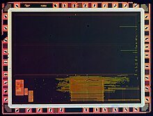
Radiation-hardened die of the 1886VE10 microcontroller before metallization etching
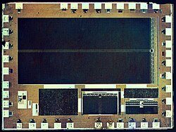
Radiation-hardened die of the 1886VE10 microcontroller after the metallization etching process
Protecting the package from radioactivity makes it easy to reduce the exposure of an exposed device.
To protect against neutron radiation and neutron activation of materials, the chips themselves can be shielded using depleted boron (consisting only of the boron-11 isotope) in the borophosphosilicate glass passivation layer that protects the chips, since natural boron-10 readily captures neutrons and undergoes alpha decay (see soft error).
Error-correcting memory (ECC memory) uses redundant bits to check and possibly correct corrupted data. Since radiation exposure damages the contents of memory even when the system is not accessing RAM, a "scrubber" circuit must continuously scan RAM, reading data, checking the redundant bits for data errors, and then writing any corrections back to RAM.
Redundant elements can be used at the system level. Three separate microprocessor boards can independently compute an answer to a calculation and compare their answers. Any system that produces the minority result will recompute. Logic can be added such that if repeated errors occur from the same system, that board is disabled.
Redundant elements can be used at the circuit level. A single bit can be replaced by three bits and separate "voting logic" for each bit, to continuously determine its result (triple modular redundancy). This increases the chip design area by a factor of 5, so it should be reserved for smaller designs. But this has the secondary advantage of also being "fault-tolerant" in real time. In the event of a failure of a single bit (which may or may not be related to radiation), the voting logic will continue to produce the correct result without resorting to a watchdog timer. Voting at the system level among three separate processor systems will generally require the use of some circuit-level voting logic to carry out the voting among the three processor systems.
Hardened latches can be used.
A watchdog timer will perform a hard reset of the system if some sequence is not executed that normally indicates the system is alive, for example, a write operation from the onboard processor. During normal operation, the software schedules writes to the watchdog timer at regular intervals to prevent the timer from expiring. If radiation causes the processor to malfunction, it is unlikely that the software will run correctly enough to clear the watchdog timer. Eventually the watchdog timer expires and forces a hard reset of the system. This is considered a last resort among the other radiation-protection methods.
The most widespread method is the "silicon-on-insulator" (SOI) technology. It consists of introducing a layer of oxygen into the surface of the substrate, which, when heated, forms a continuous silicon oxide layer approximately 0.2 µm thick. This layer insulates the CMOS channel from the silicon substrate.
Such a design reduces leakage currents and parasitic capacitances, and prevents the formation of "thyristors."
For space and military applications, it is necessary to significantly increase the hardness of the buried oxide, otherwise the gamma-radiation-induced charge migrates into the oxide over time and then recombines at the SiO2-Si interface, changing the transistor's threshold voltage. To combat this phenomenon, a path is provided for the charge to drain from the oxide-silicon contact region to the ground bus. The downside of this circuit design technique is a reduction in usable area of 30%, so it is not used in commercial applications unrelated to space activities.
The production cost of the final device manufactured using "silicon-on-insulator" (SOI) technology can exceed the production cost of conventional CMOS technology by 5-10 times.
The method is based on creating several similar devices and selecting the final value of the device state using a voting circuit based on the values at the outputs of these devices. Triplication makes it possible to completely eliminate the consequences of single failures. Radiation can change the state of such a circuit only when several nodes are affected simultaneously. However, this approach leads to an increase in the required die area and increases delays and power consumption.
There are more complex circuit designs that not only provide the correct value but also restore the state of the affected nodes — for this, feedback loops are organized.
Flip-flops are sometimes equipped with subsystems that hold them from switching for the duration of the recombination time of charges generated by an invading ion. The drawback of this method is reduced overall system speed.
Noise-immune coding: parity bits or error-correcting codes (ECC) are used by many manufacturers to protect large volumes of memory. However, when memory is exposed to relatively high-energy neutrons, secondary charged particles arise that can trigger switching of several cells at once, in which case parity checking is no longer able to detect the error.
Another approach is to store several states of the data line at some interval and then vote based on the stored states. If the storage interval is longer than the exposure time of a charged particle on the integrated circuit, then such an arrangement provides good protection against single events. However, this method is sensitive to failures on the clock line, and it also increases the node's circuit area by about a factor of three.
Radiation-hardened and radiation-tolerant components are often used in military and aerospace applications, including point-of-load (POL) applications, satellite system power supplies, step-down switching regulators, microprocessors, FPGAs, FPGA power supplies, and highly efficient low-voltage subsystem power supplies.
However, not all military-grade components are radiation-hardened. For example, the American standard MIL-STD-883 contains many radiation-related tests, but has no specification for single event latch-up rate. The Phobos-Grunt space probe may have failed due to a similar assumption.
The market for radiation-hardened electronics used in space applications is estimated at $2.35 billion in 2021. A new study has shown that by 2032 this figure will reach approximately $4.76 billion.
In telecommunications, the term "nuclear hardness" has the following meanings: 1) an expression of the degree to which the performance of a system, facility, or device is expected to degrade in a given nuclear environment, 2) the physical characteristics of a system or electronic component that will allow it to survive in an environment that includes nuclear radiation and electromagnetic pulses (EMP).

Comments