
Lecture
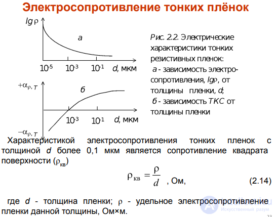
Metal films are widely used in microelectronics as interconnects, contact pads, capacitor plates, and magnetic and resistive elements of integrated circuits. The electrical properties of thin films of metals and alloys can differ significantly from the properties of bulk conductor materials. One reason for this difference is the diversity of structural characteristics of thin films obtained by condensation of molecular beams in a high vacuum. By varying the condensation conditions, the structure of the resulting films can change from an extremely disordered, finely dispersed (amorphous) state to the structure of a highly perfect single-crystal layer obtained by epitaxy. Another reason for the change in material properties in the film state is related to the manifestation of size effects. In particular, in electrical conductivity, a size effect arises when the film thickness is comparable to the electron mean free path. In this case, the resistivity of the conductor depends on the film thickness. According to Matthiessen's rule, the resistance of a thin conductor is made up of the resistivity associated with bulk scattering and the resistivity associated with scattering at the film surface:
ρ = ρB + ρS .
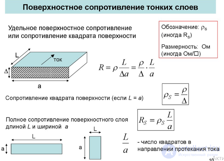
Since the nature of film nucleation and growth depends on the conditions under which the films are obtained (even with identical production methods there are many random factors), in practice it is difficult to obtain an exact match of resistivity values for films of the same thickness. Therefore, when comparing the conducting properties of thin films, the parameter sheet resistance R (or resistance per unit square, or specific surface resistance) is used, numerically equal to the resistance of a section of film whose length equals its width when current passes through its two opposite edges parallel to the substrate surface: R = ρδ /δ, where ρδ is the resistivity accounting for the size effect and δ is the film thickness.
By selecting the film thickness, R can be varied independently of the resistivity.
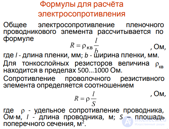
The resistance of a thin-film resistor can be calculated using the formula: R=R l/d,
where l and d are the length and width of the resistor.
For manufacturing thin-film resistors, films with a sheet resistance of 500 … 1000 Ω/square are usually required. Refractory metals (tungsten, molybdenum, tantalum, rhenium, chromium) and a nickel-chromium alloy are most commonly used as resistive materials. Film resistors made of pure metals have the advantage of being constant in composition, which makes it easier to ensure the uniformity of their structure. This leads to increased stability of electrical parameters.

Comments