
Lecture
Let us examine the processes that occur when two metallic conductors are brought together and into contact, whose energy diagrams are shown in Fig. 2.3, a. In the isolated state, the electron gas in these conductors is characterized by chemical potentials (Fermi levels) E1 and E2 and work functions χ1 and χ2. When the conductors are brought into contact, an exchange of electrons becomes possible. From Fig. 2.3, a it can be seen that in the conduction band of conductor 2 all states up to the Fermi level E2 are occupied. Opposite these states are the occupied levels of the conduction band of conductor 1. Therefore, at absolute zero, electrons from conductor 2 cannot transfer into conductor 1. At a temperature other than 0 K, electrons of conductor 2 that are thermally excited to levels above E1 can transfer into conductor 1, but the number of such electrons at ordinary temperatures is small, and the flux n21 will be weak.
A different picture arises for conductor 1. In it the conduction band is likewise filled up to the Fermi level E1, but because of the smaller work function (χ1 < χ2), opposite the occupied states of this conductor lying above the Fermi level E2 there are free levels of the conduction band of conductor 2. Therefore, when contact is present (even at absolute zero), electrons from the occupied levels of conductor 1 will transfer to the free levels of conductor 2, forming a flux n12, which at first significantly exceeds the flux n21.
Now let us examine how equilibrium is established between the conductors.
Conductor 1, losing electrons, becomes positively charged; conductor 2, gaining excess electrons, becomes negatively charged. The appearance of these charges causes a mutual shift of the energy levels of conductors 1 and 2 relative to one another. In conductor 1, which is positively charged, all levels shift downward, while in conductor 2, which is negatively charged, all levels shift upward relative to their positions in the uncharged state of these conductors (Fig. 2.3, b). This can be understood easily from the following simple reasoning. To move an electron, say, from the zero level 01 of metal 1 to the zero level 02 of metal 2, which is at a negative potential –V relative to metal 1, work numerically equal to qV must be done. This work converts into the potential energy of the electron. Therefore the potential energy of an electron at the zero level of the negatively charged conductor will be greater by ∆U = qV than the potential energy of an electron,
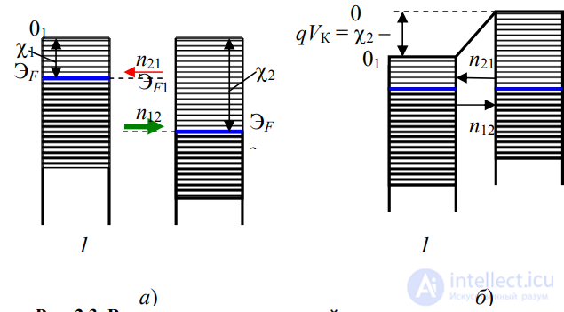
Fig. 2.3. Formation of the contact potential difference between two metals
located at the zero level of the positively charged conductor. And this means that the zero level of conductor 2 lies ∆U = qV above the zero level of the positively charged conductor.
All the energy levels of conductors 1 and 2 undergo a similar shift, including the Fermi levels EF1 and EF2.
As soon as the continuously falling Fermi level of conductor 1 (EF1) and the continuously rising Fermi level of conductor 2 (EF2) reach the same height, the cause that produced the predominant flow of electrons from conductor 1 to conductor 2 disappears, since the filled levels of conductor 1 now face filled levels of conductor 2 with the same degree of occupation. Equilibrium is established between the conductors, corresponding to an equilibrium potential difference between them, equal to
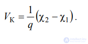
It is called the contact potential difference, determined by the difference between the work functions of the electrons from the contacting conductors. In absolute value, VK ranges from tenths of a volt to several volts. From Fig. 2.3, b, it follows that the contact potential difference creates, for electrons transferring into the conductor with the larger work function, a potential barrier of height qVK.

Comments