
Lecture
Это окончание невероятной информации про операционные усилители.
...
dual-polarity supply based on op-amps were extremely popular at the end of the last century. In modern designs, integrated power amplifiers on specialized chips prevail.
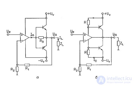
The left part of the figure shows a power amplifier on an op-amp with direct current unloading. The output transistors are connected without bias on their bases, i.e. they operate in «class B». The circuit is covered by negative feedback. The crossover distortion characteristic of this operating mode is additionally compensated by feeding signals directly from the op-amp output to the power amplifier output through resistor R3. This occurs when the output transistors are not yet open or are on the nonlinear portion of their characteristic.
The right part of the figure shows a power amplifier on an op-amp with indirect current unloading. The output transistors operate in «class AB», and the input signal of the stage is the voltage drop across resistors in the op-amp's supply circuits. The nonlinearity of the circuit is compensated by negative feedback.
In this installment of the series, we will look at how a number of op-amp circuits with frequency-dependent feedback work, and learn to build active filters and generators on op-amps.
For those who joined recently, I should mention that this is the fifth of seven installments in the series. The contents of the installments with links to them can be found at the end of the article.
We first encountered frequency-dependent feedback in op-amps when examining the behavior of real op-amps «in dynamics». It interested us in terms of frequency correction of the transfer characteristic to prevent oscillation when the op-amp operates in amplification mode, due to negative feedback turning into positive feedback because of a phase shift.
We also dealt with frequency-dependent feedback when we examined the operation of the integrating and differentiating stages. At that time we were interested not so much in the frequency response as in the response of these stages to a unit rectangular pulse.
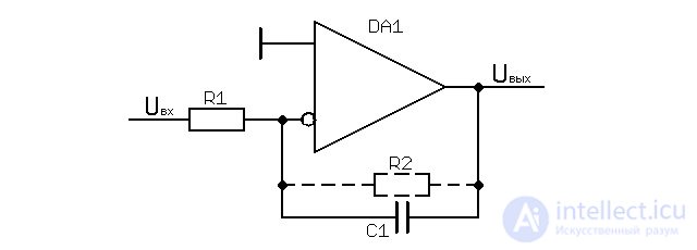
In essence, the integrating stage in the figure below has the frequency response of a 1st-order low-pass filter (LPF) with a cutoff frequency fc = 1/2πRC. A signal with a frequency below fc is passed to the output of this stage without attenuation. For frequencies above fc, the signal is passed with an attenuation of 6 dB/octave, i.e. it is attenuated by a factor of two when the frequency is doubled.
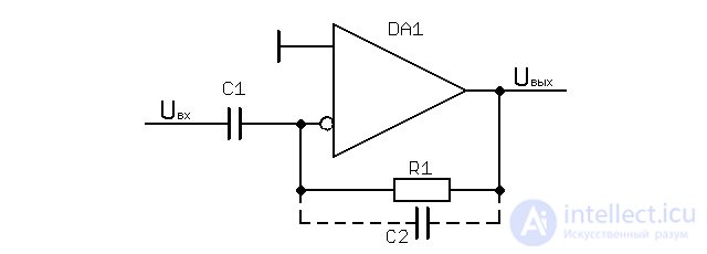
The differentiating stage is a 1st-order high-pass filter (HPF) with a cutoff frequency fc = 1/2πRC. It passes a signal with a frequency above fc without attenuation. A signal with a frequency below fc is passed with an attenuation of 6 dB/octave.
Filters are used in electronics to extract the desired component of the signal spectrum and/or to suppress an undesired one.
Initially, filters were built from passive RLC components. Active filters began to spread with the development of semiconductor electronics. Active filters are simpler to manufacture, since they do not require the use of «wound» (coil) components. However, passive filters are still used to this day.
Filter design is usually carried out using Butterworth, Chebyshev, and Bessel polynomials. Elliptic filters have been gaining popularity recently.
The topic of active filters using op-amps is covered in the greatest detail in the section «13. Active Filters» on pp. 185 – 226. Here, however, we will examine their operation using simple and accessible material presented in the section of Chapter 4, «3. Audio-frequency filters», on pp. 138 – 145, in the part dealing with op-amp circuits.
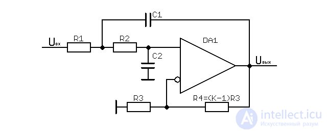
As a rule, active RC filters based on op-amps are built using the Sallen–Key topology (Sallen–Key), which acts as a «voltage-controlled voltage source» (VCVS). Below is a two-pole low-pass filter (second-order LPF) of this type:
If the resistors and capacitors are swapped, we get a two-pole high-pass filter:
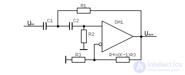
Two-pole Sallen–Key filters consist of a small number of elements and are stable in operation. The cutoff frequency is determined by the formula:
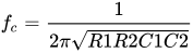 |
(20) |
The gain K is determined by the ratio of the resistances of the resistors in the feedback network. The frequency response of Sallen–Key filters changes depending on the gain. From the table on p. 290 we see that at K = 1.586 the element has a Butterworth filter response, at K = 1.268 – a Bessel filter response, and at K = 1.842 – a Chebyshev response with 0.5 dB passband ripple.
Sallen–Key filters with more than two poles behave unstably. A higher order is achieved by cascading two-pole filters. The nuances of such cascading are clearly demonstrated by Polyakov in the figure below:
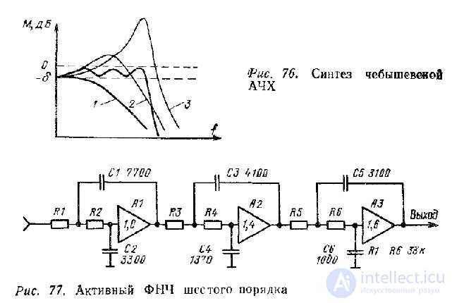
As we can see in the illustration, the frequency response of a six-pole Chebyshev LPF with a cutoff frequency of fc = 2700 Hz is formed from the response of a two-pole LPF with a cutoff frequency much lower than fc and K = 1 (labeled «1» on the graph), the response of a two-pole LPF with a cutoff frequency lower than fc and K = 1.4 (labeled «2» on the graph), and the response of a two-pole LPF with fc = 2700 Hz and K = 1.6 (labeled «3» on the graph). To reduce the effect of component tolerance on the frequency response, the ratio of the capacitor values in each stage is chosen as one to three. The resistor values are chosen from the range 10…100 kΩ.
A band-pass filter can be obtained from an HPF and an LPF with overlapping passbands. An active band-pass filter based on the Sallen–Key topology looks as follows:
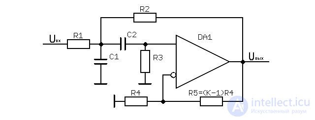
With R1 = R2, C1 = C2 and R3 = 2R1, the center frequency of the passband f0 and the filter's quality factor Q (the ratio of f0 to the passband width Δf0) are obtained from the formulas:
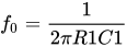 |
(21) | |
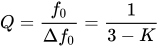 |
(22) |
From formula (22) we see that the gain K must be less than three.
Much better results can be obtained by using a biquad filter circuit as the active band-pass filter:
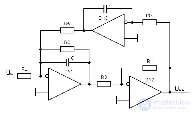
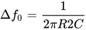
The biquad filter circuit is significantly more complex, but is less sensitive to component tolerance. The center frequency of the passband f0, the passband width Δf0, and the gain K, with R3 = R4 and R5 = R6, are determined by the formulas:
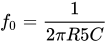 |
(23) | |
 |
(24) | |
 |
(25) |
More details on biquad filters can be found on pp. 293 – 295 and on pp. 106 – 108.
An oscillator is a device for producing periodically varying signals. A relaxation oscillator is an oscillator whose elements do not have resonant properties.
A relaxation oscillator using an op-amp can be obtained by combining an integrator circuit and a Schmitt trigger in a closed loop:
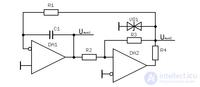
When a high-level voltage is present at the output of the Schmitt trigger, capacitor C1 charges until the voltage at the input of the Schmitt trigger becomes lower than the tripping threshold, after which capacitor C1 begins to discharge until the voltage at the input of the Schmitt trigger becomes higher than the tripping threshold.
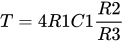
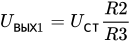
At the output of the integrating stage there is a periodic triangular-wave signal, while at the output of the Schmitt trigger there is a square wave. Zener diode VD1 limits the amplitude of the square-wave signal at the output of the Schmitt trigger Uout2 to the value of the stabilization voltage Ust. The period of self-oscillation T and the amplitude of the signal at the output of the integrating stage Uout1 are obtained from the formulas:
 |
(26) | |
 |
(27) |
Circuits of this kind are commonly called «function generators», since they produce output signals of different waveforms.
A relaxation oscillator with a square-wave output signal is called a multivibrator. The circuit considered above can also be used as a multivibrator, but the circuit shown below is simpler:
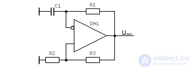
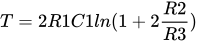
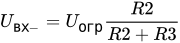
When the positive and negative clamping voltages Ulim at the op-amp output are equal, the period of self-oscillation T and the amplitude of the signal at the inverting input Uin- are obtained from the formulas:
 |
(28) | |
 |
(29) |
A sinusoidal signal at the output of an op-amp stage can be obtained by processing a triangular-wave signal with an active low-pass filter, as well as by using a Wien bridge:
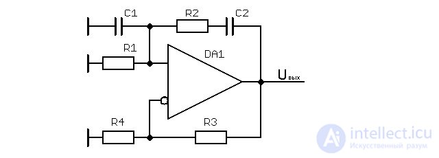
The circuit is designed to provide feedback with a phase shift of 180° at frequency f0 and to sustain oscillation by adjusting the gain K. Oscillation starts when K > 3, which is achieved when R3/R4 > 2. Then, once oscillation has started, to stabilize the oscillator's operation the gain K must decrease as the amplitude of the output signal increases. One solution for such adaptive feedback is to use an incandescent lamp instead of R4.
When R1 = R2 and C1 = C2, the oscillation frequency f0 is determined by the formula:
|
(30) |
In this installment of the series we will examine aspects of op-amp power supply, protection against interference (both at the input and via the supply), as well as protection and «decoupling» of the input circuits.
Most of the material will be worked through using a «running» example of a preamplifier-equalizer circuit with an RIAA response built around a single op-amp.
For those who have joined recently, I should mention that this is the sixth of seven articles in the series. The contents of the series, with links to them, can be found at the end of the article.
The figure below shows the circuit of an amplifier-equalizer for a magnetic phono cartridge (phono preamplifier) built around the NE5534 op-amp:
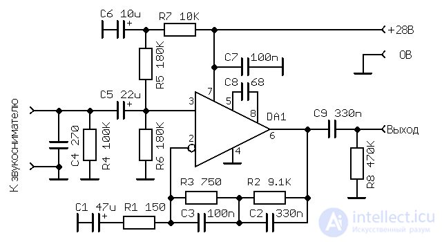
The original circuit was published on page 148. The circuit in the figure above differs from the original in the values of R3, C2, and C3, and also in that a decoupling capacitor C7, absent from the original circuit, has been added to the op-amp's power supply line.
When analyzing the circuit, two points should be highlighted:
The circuit chosen as an example is an equalizer with three corner frequencies and a high-frequency filter. A circuit of this kind of equalizer and its frequency response are shown in the figure below:
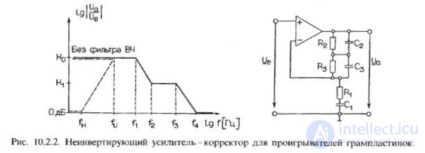
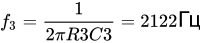
The three corner (cutoff) frequencies of the corrector are determined as:
 |
(31) | |
 |
(32) | |
 |
(33) |
The high-pass filter is designed to suppress «infra-low frequencies» (subsonic) that arise during operation of the turntable mechanism or due to record surface irregularities. The presence of this filter in phono preamps is optional. The cutoff frequency of the HPF is determined as:
 |
(34) |
The topic of correction amplifiers is discussed in detail in section «10. Frequency-Response Correction Amplifiers» on pages 122 — 148. The calculation of a corrector with three corner frequencies is given in section «10.2.2 Corrector with Three Corner Frequencies».
The phono corrector circuit shown above is an AC voltage amplifier. An AC voltage amplifier accepts only the AC component of the input signal, processes it, and passes it to the output.
With a dual (bipolar) supply, to turn any proportional stage into an AC voltage amplifier it is enough to connect the stage's input and output through coupling capacitors. With a single supply things are no longer so simple, since in that case only one half-wave of the input signal would be amplified.
To amplify the other half-wave, the input signal must be shifted so that, over the whole operating range, the amplified output signal is not clipped. In the corrector amplifier circuit, the input bias is set by the voltage divider R5R6. It is desirable, though not required, to choose R5 and R6 so as to set the voltage at the output of DA1 — equal to half the supply voltage.
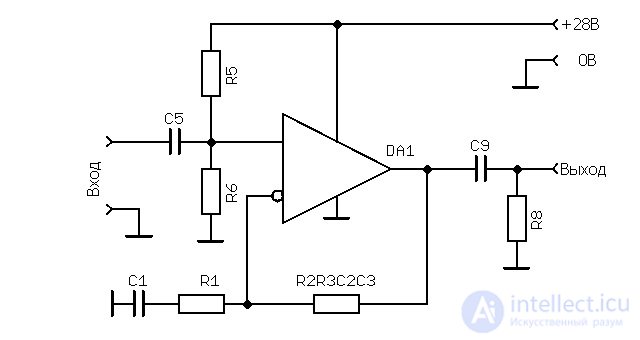
In essence, the voltage divider R5R6 forms a «virtual ground» network, which for a «classic» op-amp turns a single supply into a dual (bipolar) one.
Another important element of an op-amp amplifier circuit with a single supply is the coupling capacitor C1, which blocks the DC component of the signals in the feedback loop. Because of this, the DC transfer coefficient of the corrector amplifier is equal to unity. Having DC negative feedback in an AC voltage amplifier makes it possible to get rid of various parameter «drifts».
The presence of C1 in the circuit is «made use of» by forming, together with R1, a high-pass filter with a cutoff frequency of about 20 Hz. The capacitances of coupling capacitors C5 and C9 are chosen so as not to affect the amplifier's frequency response in the working frequency range of 20…20000 Hz: the chain C5(R5 || R6) forms a high-pass filter with a cutoff frequency of 0,1 Hz, and C9R8 — 1 Hz.
A completely non-obvious point in the design of op-amp-based devices is the fact that interference is not only external, and that the op-amp itself can be a source of interference.
This is because an op-amp, like any other electronic device, cannot change its state instantaneously. Any change of state is accompanied by transient processes, including on the supply lines.
Neither the power supply nor the conductors that carry power to it are ideal either. On top of that, the common wire of the power supply is usually used as a «signal ground», through which supply-borne interference can get into the signal circuits.
Both the power wires and the signal conductors have, besides «ohmic» resistance, inductance as well, and also capacitance relative to other conductors. That is why devices identical in circuit design but assembled from different assembly drawings can behave differently. When designing op-amp-based devices, attention must be focused on:
Taking these nuances into account, the phono preamp circuit can be drawn as follows:
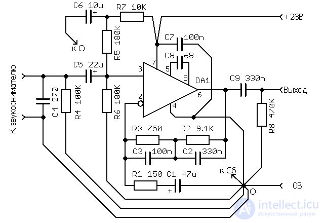
Both the power wires and the signal conductors are gathered into two «star» points, which excludes the flow of supply currents through the signal circuits. Decoupling capacitor C7 with a low ESR serves to suppress power-supply noise. The ideal case is connecting the decoupling capacitor directly to the power pins of the chip.
The low-pass filter formed by elements R7 and C6 is intended for «power-supply decoupling» of the bias circuit R5R6. «Decoupling» is intended to prevent spurious modulation of the amplifier's input via the power supply circuits.
The ratings and types of decoupling capacitors are chosen according to the datasheet of the op-amp chip's manufacturer. Recommendations on PCB layout are taken from the same source. In reality, «star» connection is usually replaced by connecting components to power ground planes.
The signal source for the phono preamplifier is an electromagnetic cartridge. The cartridge is mounted on the tonearm and connected to the phono preamp by a wired connection. The length of the connection is determined by the design of the tonearm and cannot be less than half the diameter of an «LP record» (LP, Ø300 mm).
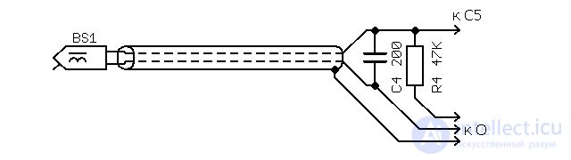
The diagram shows the connection of the electromagnetic cartridge to the phono preamp with a shielded twisted pair. The choice of a twisted pair as the connecting line is due to the fact that the EMF of the electromagnetic interference induced on such a connecting line is equal in magnitude on both wires of the line, but opposite in direction.
The twisted pair is made of thin multi-strand wires with soft insulation; the shield is a metal tube that is part of the tonearm's structure, inside which the twisted pair runs. The «return» wire of the twisted pair and the end of the shielding tube nearest the phono preamp are connected to point «O» of the preamplifier circuit.
Elements R4 and C4 are intended to match the input resistance of the phono preamp with the output resistance of the electromagnetic cartridge. Thus, for the popular GZM-005D electromagnetic cartridge, matching with the preamplifier is achieved at R4 ≈ 47 kΩ and C4 ≈ 200 pF.
In the example considered above, and in a number of other «non-industrial» applications, protection of the input circuits is not required. A coupling capacitor is sufficient as galvanic isolation, and grounding the shield of the connecting line at only one end is due solely to design considerations.
Industrial electronics impose much higher requirements. The information below is given for reference only. The subject is covered in more detail in the section «Interference, Shielding and Grounding» on pages 479–489. When designing industrial electronics, electrical safety requirements must be strictly observed.
In industrial conditions, a «star» connection or ground plane connection of the «signal» and «power» «grounds» is often impossible, since there can be a significant potential difference between these «grounds».
In this case, interference is combated by spatially separating the power and signal circuits, galvanically isolating the connecting lines, and equalizing potentials, for example, by connecting the enclosures of devices linked by a connecting line to one and the same grounding bus.
Under conditions of industrial interference, it is considered good practice to use protection of the input circuits against overvoltage and static charge, for example, as shown in the figure below:
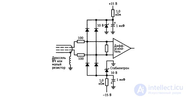
Traditionally, galvanic isolation of devices from communication lines is achieved using transformers. When isolation transformers are used, applying protection of the input circuits is also a good solution.
Under industrial conditions, using isolation amplifiers is a more expensive but also a more reliable solution.
Часть 1 Operational Amplifiers: Ideal and Real, Summing Amplifier, Differentiator, Integrator, Peak Detector
Часть 2 Frequency-dependent feedback in op-amps. Active filters and signal generators on

Comments