Lecture

Designation on schemes
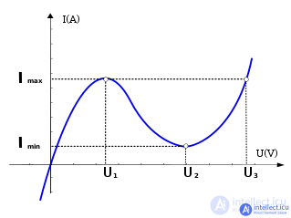
Current-voltage characteristic of the tunneling diode. In the voltage range from U1 to U2, the differential resistance is negative.
A tunnel diode is a semiconductor diode based on a degenerate semiconductor, in which, when voltage is applied in the forward direction, the tunnel effect is manifested in the appearance of a section with negative differential resistance on the current-voltage characteristic.
Conventional diodes with increasing forward voltage monotonically increase the transmitted current. In a tunnel diode, quantum-mechanical electron tunneling adds a hump to the current-voltage characteristic, and, due to the high degree of doping of the p and n regions, the breakdown voltage decreases to almost zero. The tunneling effect allows electrons to overcome the energy barrier in the transition zone with a width of 50-150 Å at such voltages when the conduction band in the n-region has equal energy levels with the valence band of the p-region. With a further increase in forward voltage, the Fermi level of the n-region rises relative to p -regions, falling on the forbidden zone of the p-region, and since tunneling cannot change the total energy of the electron, the probability of the transition of an electron from the n-region to the p-region sharply decreases. This creates a section on the direct section of the current-voltage characteristic, where an increase in the forward voltage is accompanied by a decrease in the current strength. This region of negative differential resistance is used to amplify weak microwave signals.
One of the design options for the diode is shown in Fig. 5.2. As the substrate of the GaAs structure, the most high-resistance material is used, which is usually called "semi-insulating". The epitaxial p + layer grown on the substrate is protected by a layer of SiO2 oxide. Holes of the required diameter are opened in the oxide, Sn is deposited in them to form the n + region and an Au + Ge alloy to create an ohmic contact. When the structure is heated, the deposited materials are fused; after cooling and recrystallization, the n + region of the tunnel diode is formed. At the required points, metal ball contacts are soldered to which the external terminals subsequently contact. Variants of the design of diodes with beam terminals are also common.
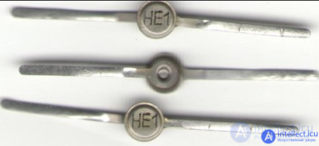
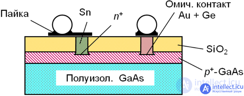
Fig. 5.2. Tunnel Diode Design Option
In the early 1920s in Russia, Oleg Losev discovered the cristadine effect in diodes made of crystalline ZnO grown hydrothermally from an aqueous solution of zinc hydroxide and potassium zincate — the effect of negative differential resistance.
For the first time, a tunneling diode was made on the basis of Ge in 1957 by Leo Esaki, who in 1973 received the Nobel Prize in physics for the experimental discovery of the effect of electron tunneling in these diodes.
Tunnel diodes with very low resistance are classified as degenerate. they have:
The unique properties of the tunneling diode are manifested in its current-voltage characteristic (CVC) with forward bias in the semiconductor.
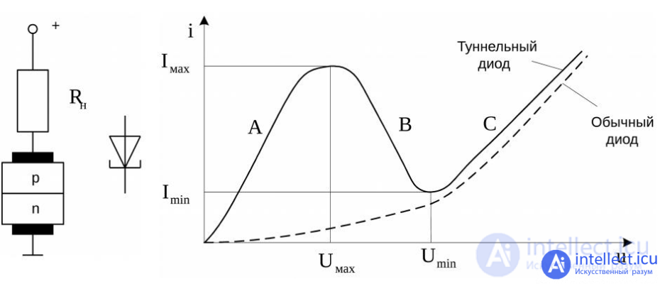
The diagram shows that in section A, the current increases with increasing voltage. In section B, the semiconductor exhibits negative resistance (tunneling effect), which leads to the fact that with an increase in the voltage characteristic, the current decreases. In section C, the device again provides a direct relationship between current and voltage.
Tunnel diodes are designed to work just on the segment, which is characterized by negative resistance. A slight increase in voltage turns it off, and a decrease - turns it on.
When choosing this semiconductor take into account:
Advantages of tunnel diodes:
All tunnel diodes are compact in size. Often they are products in sealed cases of cylindrical shape with a diameter of 3-4 mm, a height of 2 mm and a weight of less than 1 gram.
A significant drawback of semiconductors of this type is significant aging, which leads to a change in their properties, and therefore to a violation of the normal functionality of the device. “Tunnels” can lose their previous parameters not only because of exceeded operating conditions, but even because of long-term storage, after which they turn into “inverted” semiconductors. This circumstance often causes the malfunctioning of industrial oscilloscopes.
There are also “inverted” industrial semiconductors. They differ from tunnel ones by a lower concentration of impurities, although the general principle of their functioning is the same.
It is forbidden to check the operability of the tunnel diode by an avometer - a combined device for measuring current, voltage and frequency, since semiconductors of some groups can fail. If it is not known that the part belongs to a certain category, then it is safer to use a generator probe, which allows you to monitor the efficiency of the tunnel diode in active mode.
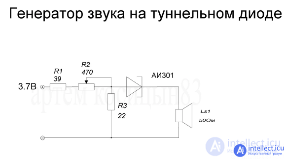
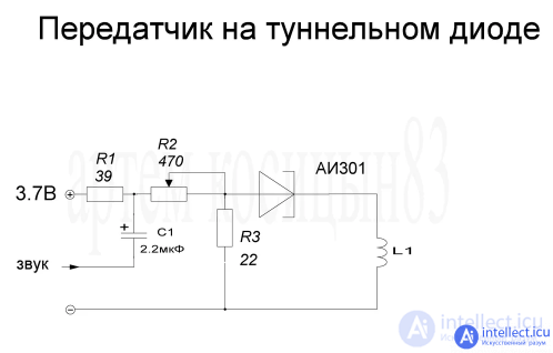
The most widely used in practice are tunnel diodes from Ge, GaAs, and also from GaSb. These diodes are widely used as generators and high-frequency switches, they operate at frequencies many times higher than the frequency of the tetrodes, up to 30 ... 100 GHz.
Comments
To leave a comment
Electronics, Microelectronics, Element Base
Terms: Electronics, Microelectronics, Element Base