Lecture
A thyristor is a semiconductor device based on a single crystal with a four-layer structure with three p-n junctions and possessing valve properties, i.e. a device that allows current to pass in one direction with the ability to control its average and effective value by controlling the thyristor switching phase.
A thyristor is a semiconductor device that has two stable states: a closed state, that is, a state of low conductivity, and an open state, that is, a state of high conductivity.
A thyristor can be considered as an electronic switch (key). The main application of thyristors is to control a powerful load using weak signals, as well as switching devices. There are different types of thyristors, which are divided mainly by the control method and by conductivity. The difference in conductivity means that there are thyristors that conduct current in one direction (for example, the triac shown in the figure) and in two directions (for example, triacs, symmetrical dinistors ).
Dinistor (other names: diode thyristor , Shockley diode , not to be confused with Schottky) is a solid-state trigger device with two terminals, which is a pnpn semiconductor structure and demonstrates an S-shaped volt-ampere characteristic at the operating polarity of the external voltage. It functions as a thyristor, but without control electrodes. It is widely used in power semiconductor electronics as a switch; new dinistor designs continue to be created.
The thyristor has a nonlinear volt-ampere characteristic (VAC) with a section of negative differential resistance. Compared, for example, with transistor keys, thyristor control has some features. The transition of the thyristor from one state to another in an electric circuit occurs abruptly (avalanche-like) and is carried out by an external effect on the device: either voltage (current) or light (for a photothyristor). After the thyristor transitions to the open state, it remains in this state even after the control signal has ceased, if the current flowing through the thyristor exceeds a certain value, called the holding current.
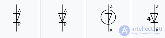
Thyristor designations
|
Name |
Designation |
|
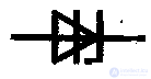
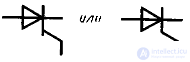
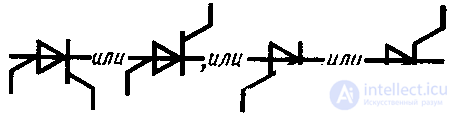
1. Thyristor diode, reverse-locked |
|
|
2. Thyristor diode, conducting in the reverse direction |
|
|
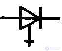
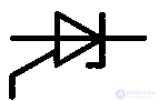
3. Symmetrical diode thyristor |
|
|
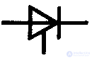
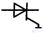
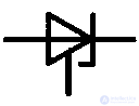
4. Triode thyristor. General designation |
|
|
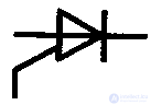
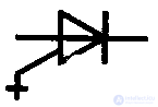
5. Thyristor triode, reverse locked with control: by anode |
|
|
by cathode |
|
|
6. Triode thyristor with switch-off: general designation |
|
|
reverse locking, anode controlled |
|
|
reverse locking, cathode controlled |
|
|
7. Reverse conducting triode thyristor: general designation |
|
|
anode controlled |
|
|
cathode controlled |
|
|
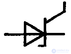
8. Symmetrical triode thyristor (bidirectional) - triac |
|
|
9. Thyristor tetroid, reverse locked |
|
Note: It is permissible to depict the designation of an anode-controlled thyristor as a continuation of the corresponding side of the triangle.
The control electrode allows controlling the moment of switching on the thyristor even with a positive potential difference between the anode and cathode less than the breakdown potential, if a direct current is created through the 1st pn junction. The moment of switching on, or the switching phase, is called the control angle .
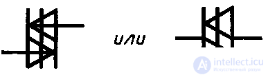
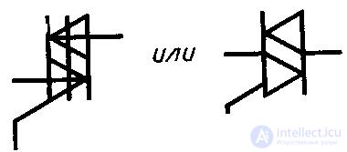
There is no single generally accepted designation for a dinistor as an element of an electric circuit. Possible symbol options are presented below:
Some symbols of the dinistor are formed by drawing the number 4, according to the number of layers in the structure . This is especially visible if you rotate the third drawing from the left by 180 0 (see the photo of the "monument" to the dinistor).
An important parameter of the thyristor is the control current Iупр – the current of the control electrode, which ensures switching the thyristor to the open state.
Some thyristors can switch very high currents, in this case they are called power thyristors. They are made in a metal case - for better heat dissipation. Small models with a plastic case are usually low-power options that are used in low-current circuits. But there are always exceptions. So for each specific purpose, the required option is selected. They are selected, of course, by parameters. Here are the main ones:
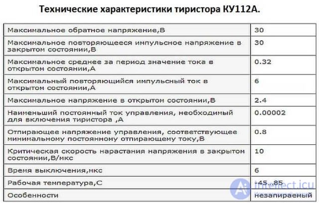
Example of characteristics
There is also a dynamic parameter - the time of transition from the closed to the open state. In some schemes, this is important. The type of speed may also be specified: by unlocking time or by locking time.
Thyristors have found wide application due to a number of advantages over diodes:
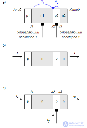
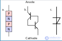
Fig. 1. Thyristor circuits: a) Basic four-layer pnpn structure b) Diode thyristor c) Triode thyristor.
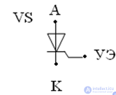
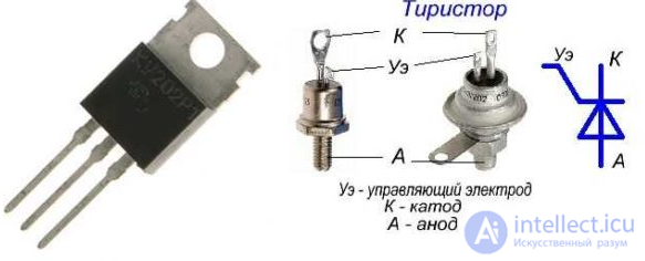
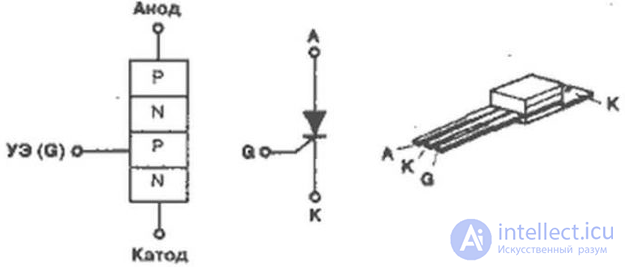
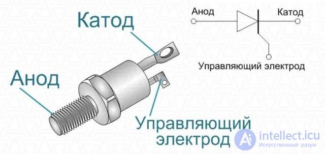
The basic diagram of the thyristor structure is shown in Fig. 1. It is a four-layer semiconductor of the pnpn structure , containing three series-connected pn -junctions J1, J2, J3. The contact to the outer p -layer is called the anode, to the outer n- layer - the cathode. In general, a pnpn device can have up to two control electrodes (bases) connected to the inner layers. By applying a signal to the control electrode, the thyristor is controlled (changed its state). A device without control electrodes is called a diode thyristor or dinistor . Such devices are controlled by voltage applied between the main electrodes. A device with one control electrode is called a triode thyristor or thyristor (sometimes simply a thyristor, although this is not entirely correct). Depending on which layer of the semiconductor the control electrode is connected to, thyristors can be anode-controlled or cathode-controlled. The latter are the most common.
The devices described above come in two varieties: those that pass current in one direction (from the anode to the cathode) and those that pass current in both directions. In the latter case, the corresponding devices are called symmetrical (since their I-V characteristic is symmetrical) and usually have a five-layer semiconductor structure. A symmetrical thyristor is also called a triac or simistor . It should be noted that instead of symmetrical dinistors , their integral analogs are often used, which have better parameters.
Thyristors with a control electrode are divided into locking and non-locking. Non-locking thyristors, as the name suggests, cannot be switched to the closed state by a signal applied to the control electrode. Such thyristors close when the current flowing through them becomes less than the holding current. In practice, this usually happens at the end of the half-wave of the mains voltage.
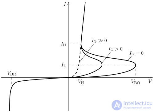
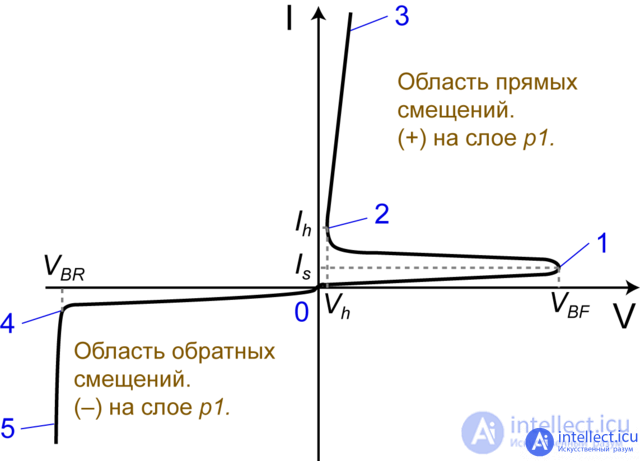
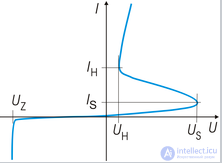
Fig. 2. Volt-ampere characteristic of a thyristor
A typical I–V characteristic of a thyristor conducting in one direction (with or without control electrodes) is shown in Fig. 2. It has several sections:
The volt-ampere characteristic of symmetrical thyristors differs from that shown in Fig. 2 in that the curve in the third quarter of the graph repeats sections 0-3 symmetrically relative to the origin.
According to the type of nonlinearity of the current-voltage characteristic, the thyristor is classified as an S-device.
Reverse locking mode
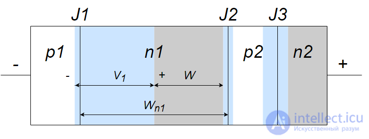
Fig. This is stated on the website https://intellect.icu . 3. Thyristor reverse locking mode
Two main factors limit the reverse breakout and forward breakout modes:
In the reverse blocking mode, a voltage negative with respect to the cathode is applied to the anode of the device; junctions J1 and J3 are reverse biased, and junction J2 is forward biased (see Fig. 3). In this case, most of the applied voltage drops across one of the junctions J1 or J3 (depending on the degree of doping of the various regions). Let this be junction J1. Depending on the thickness Wn1 of the n1 layer, breakdown is caused by avalanche multiplication (the thickness of the depletion region during breakdown is less than Wn1) or by puncture (the depletion layer spreads over the entire n1 region, and junctions J1 and J2 close).
In forward blocking, the voltage at the anode is positive with respect to the cathode and only junction J2 is reverse biased. Junctions J1 and J3 are forward biased. Most of the applied voltage drops across junction J2. Minority carriers are injected through junctions J1 and J3 into the regions adjacent to junction J2, which reduce the resistance of junction J2, increase the current through it and reduce the voltage drop across it. As the forward voltage increases, the current through the thyristor initially grows slowly, which corresponds to the 0-1 section on the I-V characteristic. In this mode, the thyristor can be considered blocked, since the resistance of junction J2 is still very high. As the voltage across the thyristor increases, the proportion of the voltage dropping across J2 decreases and the voltages across J1 and J3 increase faster, which causes a further increase in the current through the thyristor and an increase in the injection of minority carriers into the J2 region. At a certain voltage value (of the order of tens or hundreds of volts), called the switching voltage VBF (point 1 on the I-V characteristic), the process takes on an avalanche-like character, the thyristor goes into a state with high conductivity (turns on), and a current is established in it, determined by the voltage of the source and the resistance of the external circuit.
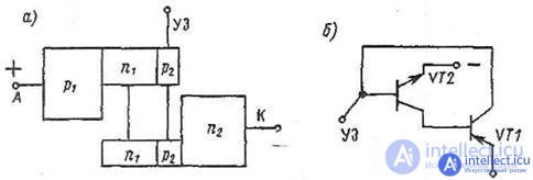
Two-transistor model
To explain the characteristics of the device in the forward blocking mode, a two-transistor model is used. The thyristor can be viewed as a junction of a pnp transistor with an npn transistor, with the collector of each connected to the base of the other, as shown in Fig. 4 for a triode thyristor. The central junction acts as a collector of holes injected by junction J1 and electrons injected by junction J3. The relationship between the emitter IE , collector IC , and base IB currents and the static current gain α1 of the pnp transistor is also shown in Fig. 4, where ICo is the reverse saturation current of the collector-base junction.
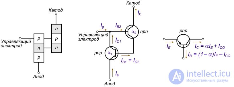
Fig. 4. Two-transistor model of a triode thyristor, connection of transistors and ratio of currents in a pnp transistor.
Similar relationships can be obtained for an npn transistor when changing the direction of the currents to the opposite. From Fig. 4 it follows that the collector current of an npn transistor is simultaneously the base current of a pnp transistor. Similarly, the collector current of a pnp transistor and the control current Ig flow into the base of the npn transistor. As a result, when the total gain in the closed loop exceeds 1, the regenerative process becomes possible.
The base current of a pnp transistor is  . This current also flows through the collector of an npn transistor.
The collector current of an npn transistor with a gain  of
of
Equating  and
and  , we get:

Because something like  this:
this:

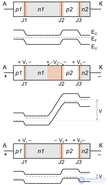
Fig. 5. Energy band diagram in forward bias mode: equilibrium state, forward blocking mode and forward conduction mode.
This equation describes the static characteristic of the device in the voltage range up to breakdown. After breakdown, the device operates as a pin diode. Note that all terms in the numerator of the right-hand side of the equation are small, therefore, while the term α1 + α2 < 1, the current IA is small. (The coefficients α1 and α2 themselves depend on IA and usually increase with increasing current) If α1 + α2 = 1, then the denominator of the fraction becomes zero and direct breakdown (or thyristor switching on) occurs. It should be noted that if the polarity of the voltage between the anode and cathode is changed to the opposite, then junctions J1 and J3 will be shifted in the reverse direction, and J2 - in the forward direction. Under such conditions, breakdown does not occur, since only the central junction operates as an emitter and the regenerative process becomes impossible. It can also be noted that the two-transistor model is used not only to study the processes occurring in the thyristor, but also as its circuit analogue in electronic equipment.
The widths of the depletion layers and the energy band diagrams at equilibrium, in the forward blocking and forward conduction modes are shown in Fig. 5. At equilibrium, the depletion region of each junction and the contact potential are determined by the impurity distribution profile. When a positive voltage is applied to the anode, junction J2 tends to be reverse biased, and junctions J1 and J3 tend to be forward biased. The voltage drop between the anode and cathode is equal to the algebraic sum of the voltage drops across the junctions: VAK = V1 + V2 + V3 . As the voltage increases, the current through the device increases and, consequently, α1 and α2 increase. Due to the regenerative nature of these processes, the device will eventually go into the open state. After the thyristor is turned on, the current flowing through it must be limited by the external load resistance, otherwise the thyristor will fail at a sufficiently high voltage. In the on state, junction J2 is forward biased (Fig. 5, c), and the voltage drop VAK = (V1 - | V2 | + V3) is approximately equal to the sum of the voltage on one forward biased junction and the voltage on the saturated transistor.
When the thyristor is in the on state, all three junctions are forward biased. Holes are injected from the p1 region and electrons from the n2 region, and the n1-p2-n2 structure behaves like a saturated transistor with the diode contact to the n1 region removed. Therefore, the device as a whole is similar to a pin (p+-i-n+) diode…
dU/dt effect
When applying a voltage of direct polarity to the anode and cathode of the thyristor at a speed greater than some critical dU/dt> dUcrit/dt, the pnpn structure will open. The mechanism of this effect is due to the presence of parasitic capacitance anode-control electrode. This effect limits the use of thyristors in high-frequency circuits, although it is sometimes used to control the thyristor. The parameter dUcrit/dt is specified in reference books for each thyristor model.
If the current flowing through the thyristor in the forward direction (in the open state) increases at a rate greater than some critical value di/dt > dicrit/dt, then the structure will be destroyed and the thyristor will fail, which is explained by the limited growth of the carrier flow area, the increase in current density and local thermal breakdown. The dicrit/dt parameter is a reference parameter and is specified in the catalogs for each thyristor model.
Classification of thyristors:
• Dinistor, without a control electrode; only anode and cathode
• Trinistor, with a control electrode
• Semicistor, bidirectional thyristor.
By conductivity and number of terminals:
Previously, thyristors were called “controlled diodes” in domestic literature.
There are no fundamental differences between a dinistor and a trinistor, however, if the opening of a dinistor occurs when a certain voltage is reached between the terminals of the anode and cathode, depending on the type of the dinistor, then in a trinistor the opening voltage can be specially reduced by applying a current pulse of a certain duration and magnitude to its control electrode with a positive potential difference between the anode and cathode, and structurally the trinistor differs only in the presence of a control electrode. Trinistors are the most common devices from the "thyristor" family.
Switching to the closed state of conventional thyristors is carried out either by reducing the current through the thyristor to the value Ih , or by changing the polarity of the voltage between the cathode and the anode.
Lockable thyristors, unlike conventional thyristors, can switch from the closed state to the open state and vice versa under the influence of the control electrode current. To close a lockable thyristor, it is necessary to pass a current of the opposite polarity through the control electrode than the polarity that caused it to open.
Semiconductor technologies are still being developed and improved. Over the past few decades, new varieties of thyristors have appeared, which have some differences.
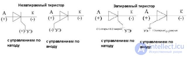
Thyristors can be controlled from both the anode and the cathode.
There are also different types of thyristors by the method of locking. In one case, it is enough to reduce the anode current below the level of the holding current. In the other case, a locking voltage is applied to the control electrode.
We said that thyristors conduct current only in one direction. There is no reverse conductivity. Such elements are called reverse-non-conductive, but there are not only such. There are other options:

They are distinguished mainly by the type of conductivity and control method.
Thyristors can operate in the key mode. That is, when a control pulse is received, they supply current to the load. The load, in this case, is calculated based on the open-state voltage. It is also necessary to take into account the greatest dissipated power. In this case, it is better to choose metal models in the form of a "flying saucer". It is convenient to attach a radiator to them - for faster cooling.
The following subtypes of thyristors can also be distinguished:

The main purpose is to turn on and off a powerful load using low-power control signals
The main area of application of thyristors is as an electronic key, used to close and open an electric circuit. In general, many familiar devices are built on thyristors. For example, a garland with running lights, rectifiers, pulse current sources, rectifiers and many others.
9.1) In terms of the operating principle, a thyristor can also be compared to a diode. It will pass current in one direction - from the anode to the cathode, but this will only happen in the "open" state. In diagrams, a thyristor looks like a diode. It also has an anode and a cathode, but there is also an additional element - a control electrode. It is clear that there are differences in the output voltage (if compared with a diode).
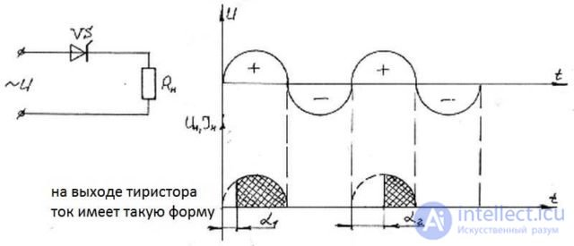
The principle of operation of the thyristor in AC devices: at the output there is only the upper part of the sinusoid
In AC circuits, the thyristor will only pass one half-wave - the upper one. When the lower half-wave arrives, it resets to the "closed" state.
9.2) Let us consider the operating principle of the thyristor.
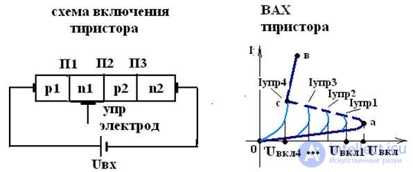
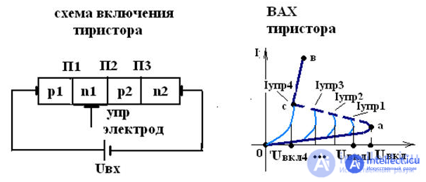
When voltage Uin is applied to the thyristor anode, junctions P1 and P3 are open, and junction P2 is closed, therefore the entire input voltage is applied to the locked layer P2. As a result, the thyristor current is very small. As the input voltage increases, the current through the thyristor will increase slightly until junction P2 breaks down; the breakdown voltage is called the turn-on voltage
Uin = Ubreakdown = Uon (point a). Segment |0a| is the reverse branch of junction P2. When junction P2 breaks down, the current through the thyristor increases sharply (point b). Segment |vc| all three junctions are under the input voltage, since the voltages of junctions P1 and P3 are the same, but opposite in sign. Segment |ac| is the section of "negative" resistance of the thyristor.
If current is applied to the control electrode, the breakdown voltage of the thyristor can be changed. The higher the control current, the lower the thyristor turn-on voltage, i.e. the thyristor will turn on earlier.
Iupr4 > Iupr3 > Iupr2 > Iupr1 > 0, therefore Uon4
Usually, a thyristor is represented as two transistors connected to each other, each of which operates in the active mode.
In connection with such a pattern, we can call the extreme regions - emitter, and the central junction - collector.
To understand how a thyristor works, it is worth looking at the volt-ampere characteristic.
A small positive voltage was applied to the thyristor anode. This is stated on the website https://intellect.icu . The emitter junctions are connected in the forward direction, and the collector junction in the reverse direction. (In fact, all the voltage will be on it). The section from zero to one on the volt-ampere characteristic will be approximately similar to the reverse branch of the diode characteristic. This mode can be called the closed state mode of the thyristor.
With an increase in the anode voltage, the injection of the main carriers into the base region occurs, thereby accumulating electrons and holes, which is equivalent to the potential difference at the collector junction. With an increase in the current through the thyristor, the voltage at the collector junction will begin to decrease. And when it decreases to a certain value, our thyristor will go into the state of negative differential resistance (section 1-2 in the figure).
After that, all three transitions will be shifted in the forward direction, thereby transferring the thyristor to the open state (section 2-3 in the figure).
The thyristor will be in the open state as long as the collector transition is biased in the forward direction. If the thyristor current is reduced, then as a result of recombination, the number of nonequilibrium carriers in the base regions will decrease and the collector transition will be biased in the reverse direction and the thyristor will go into the closed state.
When the thyristor is turned on in the reverse direction, the volt-ampere characteristic will be similar to that of two series-connected diodes. The reverse voltage will be limited in this case by the breakdown voltage.
In circuits with alternating voltage, as a rule, the thyristor is reset according to the second option. Alternating current in a household network has a sinusoidal shape, when its value approaches zero, a reset occurs. In circuits powered by direct current sources, it is necessary to either forcibly remove the power supply or remove the load.
After the release voltage is removed, the thyristor remains in the open state (the light is on)
That is, the thyristor works differently in circuits with constant and alternating voltage. In a constant voltage circuit, after a short-term appearance of voltage between the anode and the control terminal, the element goes into the "open" state. Then there can be two possible scenarios:
So in DC circuits there are two options for using a thyristor - with and without maintaining an open state. But the first type is more often used - when it remains open.
If we talk about the internal structure, then these are three PNPN transitions
The operating principle of a thyristor in alternating voltage circuits is different. There, the return to the locked state occurs "automatically" - when the current drops below the holding threshold. If the voltage is applied to the anode-cathode constantly, we get current pulses at the thyristor output, which go with a certain frequency. This is how pulse power supplies are built. With the help of a thyristor, they convert a sinusoid into pulses.
Rectifiers that combine rectification of alternating voltage with control of the rectified voltage are called control rectifiers.
The main element of a controlled rectifier is a thyristor.
Voltage control is reduced to time control of the moment of thyristor opening.
Classification of controlled rectifiers
• single-phase, single-half-wave
• single-phase bridge: with a full number of thyristors and with an incomplete number, i.e. 2 thyristors, 2 diodes
• three-phase with output from the midpoint of the transformer and bridge.
Depending on the number of terminals, it is possible to derive a classification of thyristors. In essence, everything is very simple: a thyristor with two terminals is called a dinistor (accordingly, it has only an anode and a cathode). A thyristor with three and four terminals is called a triode or tetrode. There are also thyristors with a large number of alternating semiconductor regions. One of the most interesting is a symmetrical thyristor (triac), which turns on at any voltage polarity.
Half-wave controlled rectifier
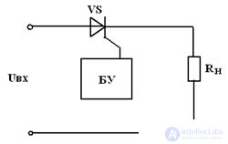
БУ – control unit The control current in the positive half-period e(t) opens the 1st pn junction and turns on the thyristor. In the negative half-period, opening the 1st pn junction does not lead to opening the 3rd pn junction, because the diffusing carriers do not reach it, as they have time to recombine almost completely.
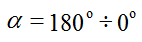
The average and effective value of the rectified current (voltage) can be regulated within a wide range by changing the phase of the control current supply.
The presented circuit includes a control circuit, which significantly complicates it, since it requires fairly accurate synchronization in frequency of the control current with the frequency of the rectified voltage.
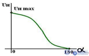
Timing diagrams
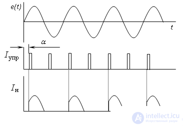
Regulation of the average voltage at the rectifier output for a half-wave rectifier
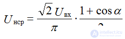
the voltage can be regulated within the limits
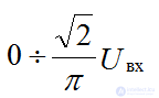
by changing the regulation angle
for a full-wave rectifier
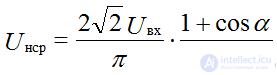
the regulation characteristic of the controlled rectifier
A) structure;
b) equivalent circuit;
c) dinistor designation
The dinistor has four regions, three pn junctions . The outer regions are called emitters, the inner ones are called bases, the outer pn junctions are called emitter junctions, and the inner one is called collector junctions. The device has two electrodes: a cathode (from the n-emitter side) and an anode (from the p-emitter side).
The volt-ampere characteristic (VAC) of a dinistor, like the VAC of a thyristor, is S-shaped. The dinistor has current bistability in the voltage range from the holding voltage U H to the turn-on voltage U S . In this range, two states of the device with different current values correspond to the same voltage value: blocking and conducting. In the blocking state, the voltage is mainly applied to the reverse-biased collector pn junction, the concentration of nonequilibrium carriers in the bases is insignificant. In the conducting state, all three pn junctions have a forward bias, nonequilibrium carriers are injected into the bases. At a sufficiently high current density, the device operates like a diode with a long base under forward bias: the base regions are filled with high-concentration electron-hole plasma injected from the emitters. The voltage drop across the base regions in this mode can significantly exceed the bias of the pn junction barriers.
The mechanism of bistability of the dinistor is the same as that of the thyristor. This mechanism is determined by the nonlinear interaction of three pn junctions of the pnpn structure. The transition to the conducting state is associated with a change in the polarity of the collector junction bias from reverse to direct with an increase in current density. The mechanism of interaction of three p-n junctions is explained by the two-transistor model (see the article Thyristor), within which the pnpn structure is presented as two "composite" pnp and npn transistors in accordance with the equivalent circuit of the dinistor shown in the figure. The two-transistor model relates the turn-on voltage U S with the transfer coefficients of the "composite" transistors.
To turn on a dinistor, as well as a thyristor, it is necessary to introduce excess nonequilibrium carriers into the bases of the pnpn structure — the so-called "starting" or "control" charge. The value of this charge must exceed the critical charge Q s , which characterizes a specific pnpn structure. The critical charge Q s has a characteristic surface density of about 10 -6 C/cm 2 . Unlike a thyristor, a dinistor does not have a control electrode (gate), which allows introducing a control charge using the gate current. Therefore, other methods are used in practice to switch a dinistor. These include, in particular, an avalanche breakdown of the collector junction or a "puncture" (complete depletion) of the base, causing the injection of carriers from the emitter.
The S-shaped I-V characteristic is associated with the phenomenon of hysteresis: when the voltage increases, the device is in the blocking state up to the turn-on voltage U S , when it decreases, it remains in the conducting state until the holding voltage U H is reached , and U H < U S . For the experimental observation of this phenomenon in a dinistor, a series ohmic resistance is required, limiting the current value at high voltages. The states of the device in this case are specified by the intersection of the I-V characteristic and the load line.
For a dinistor, as well as other devices with an S-shaped current-voltage characteristic, the phenomenon of current pinching, which is undesirable in practice, is characteristic .

In the 1950s, the dinistor was one of the first silicon (not germanium) devices ; a "monument" to this device was erected in California in connection with its historical significance.
Then for many years it was widely used in circuit engineering as a key, for example, to create a thyristor unlocking pulse. Due to the simplicity of the design and low cost, it was considered an ideal element in the circuit of a thyristor power regulator or pulse generator.
Since the 1990s, for low-current applications, it has been displaced from the market by elements such as the diac.
Nowadays, dinistors are used mainly in power semiconductor electronics; new dinistor designs and voltage supply algorithms are being developed for this area.
The specificity of powerful dinistors consists of a number of design features and the choice of layer parameters, including weak base doping to increase the turn-on voltage and a large area of devices. A specially developed current supply order must be used.
Thus, in a reversibly switched dinistor (RSD) — a power pulse device — a small current pulse of reversible (i.e. non-working) polarity is first supplied, when the bases, primarily the n-base, are filled with electron-hole plasma through a forward-biased collector junction. After this, already with working polarity, the dinistor is switched on more easily than without preliminary pumping, as if the control electrode current were supplied to the thyristor. The advantage is the simultaneous switching on over the entire area at once.
Such devices are currently made using silicon (Si), and the possibility of using silicon carbide (SiC) for high-temperature applications is also being discussed.
You can check the thyristor either with a multimeter or by creating a simple test circuit. If you have the technical specifications in front of you when checking, you can also check the resistance of the transitions.
One of the types: power T122-25
First, let's analyze the multimeter's continuity test. Switch the device to continuity test mode.
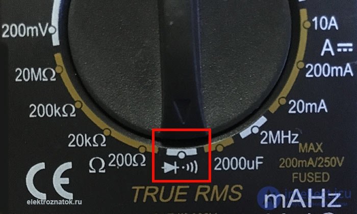
Digital multimeters have a continuity test mode that allows you to check semiconductor devices.
Next, we touch the probes to the pairs of terminals one by one:
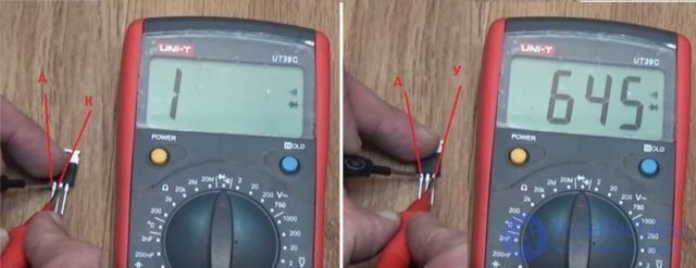
Checking the thyristor with a multimeter. In the left picture, the display shows "1", i.e. the resistance between the anode and cathode is too high and the device cannot record it. In the right picture, the resistance is low, since a direct bias voltage is applied between the anode and the control electrode.
Please note that the resistance value varies between series - you shouldn't pay much attention to this. If you want to check the transition resistance, look in the technical specifications.
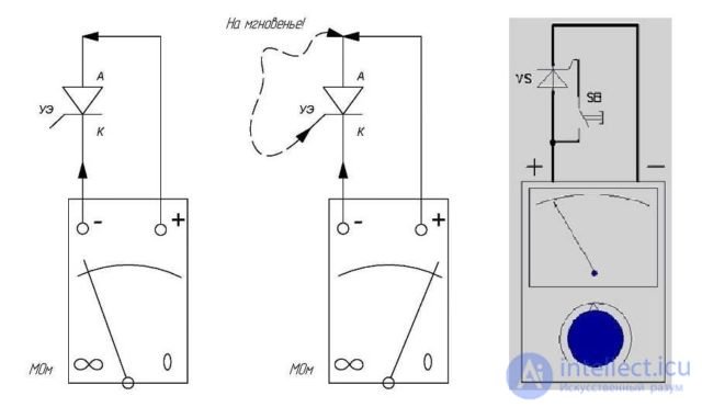
Scheme for checking the thyristor performance with a multimeter
The figure shows the test circuits. The figure on the far right is an improved version with a button that is installed between the anode and the control terminal. In order for the multimeter to record the current flowing through the circuit, we press the button briefly.
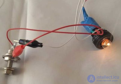
If you don't have a multimeter, you can check the thyristor using a light bulb and a power source. Even a regular battery or any other source of constant voltage will do. But the voltage must be sufficient to light the bulb. You will also need a resistor or a regular piece of wire. A simple circuit is assembled from these elements:
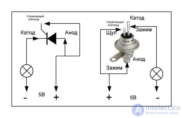
Scheme of testing a thyristor using a light bulb and a power source
Along with the check, this diagram allows you to understand the principle of the thyristor. After all, the picture is very clear and understandable.

Comments