Lecture
In the case of topological design, IET are usually replaced with their installation models. The IET seat is a projection of the installation model on the board.
An approximate estimate of the possibility of locating IET with seating areas S i on a 5 ”board can be made using the so-called analytical layout. Board area
 (16.1)
where K Sj = 0.5. ..0.9 — filling factor of the area of the j- th board, taking into account the space for laying the tracks, contact pads and other; Nj - the number of IET on the j - th the board.

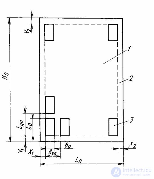
Fig. 16.1. Placing IET on the board:
1 - placement area; 2 - marginal fields; 3 - IET.
In most cases, the boards have a rectangular shape, and the product of the sizes of the sides must correspond to the area, and their ratio is usually less than 3: 1. Linear board sizes should be rounded to standard or acceptable standardized values in this design.
The IET can be placed not over the entire surface of the board, but only in the placement area (fig. 7.2). The width of the edge zones Y 1 , Y 2 is determined either by microcracks and defects arising during the machining of the ends of the boards, or by the peculiarities of its installation in the supporting structures; X 1 - front panel mounting area; Zone X 2 in modules of detachable design is occupied by the connector, and one-piece is the zone for soldering external connections.
In topological design, the placement area is considered as part of a continuous or discrete mounting plane. In the case of continuous IET planes, arbitrary coordinates of the anchor may have discrete coordinates, and they are divided into positions for IET installation.
It is recommended to have MI C on the board in rows and columns [7.1]. Number of columns
 (16.2)
where E | ... | is the symbol of integer rounding; L 0 - the width of the seat IC; L X0 is the step for installing the microcircuits along the X axis . Number of rows
 (16.3)
where l 0 is the length of the chip seat; l Y0 - step installation of microcircuits along the Y axis .
The IC installation step determines a large number of factors: the complexity of the concept, the average number of conclusions involved, the requirements for packing density, the temperature regime, the design method (manual or automated), etc. installation is growing.
The spatial orientation of the IC should take into account the direction of the cooling air flow during natural cooling. Since the boards are more often installed vertically, with natural cooling, large sides of the housings with terminals are arranged parallel to the side of the board on which the connector is installed.
In modules of digital RES in a detachable design, it is advisable to place IET in the first column from the connector, as closely as possible connected with it, in the next — with the connector and with the elements already placed, and so on until the placement is complete. In an electronic distribution system with an unbranched structure, a linear arrangement is adopted, in which the cascades are placed one after the other from the device input to the output, which, by increasing the separation of potential sources and pickups, improves EMC.
Comments
To leave a comment
Design and engineering of electronic equipment
Terms: Design and engineering of electronic equipment