A stepped microwave impedance transformer consisting of cascaded stages with parallel-connected quarter-wave sections of coupled strip lines having different characteristic impedances, characterized in that the electromagnetic coupling between the aforementioned stages is provided by the aforementioned quarter-wave sections by means of their electrical connection being made in a cascaded parallel connection of the aforementioned lines using jumpers, whereby the line representing the first high-impedance stage is electromagnetically coupled to two lines connected in parallel with it by means of the first and second parallel jumpers, these two lines constituting the second stage and being electromagnetically coupled to two other lines, also connected in parallel by means of the first and third parallel jumpers, these two other lines constituting the third low-impedance stage.
patent number RU2582052C2 2014-07-02 Application filed by Federal State Budgetary Educational Institution of Higher Professional Education "Moscow State Technical University of Civil Aviation" (MSTU CA)
The invention relates to microwave engineering and can be used in the design of miniature microwave transforming devices.
The purpose of the invention is to reduce the dimensions and increase the frequency passband of a microwave transformer.
The closest analog to the proposed transformer is the multistage transformer (Feldstein A.L., Yavich L.R. Synthesis of Two-Port and Four-Port Networks at Microwave Frequencies. - Moscow: Svyaz, 1971). The advantage of the multistage transformer is its wide frequency band, while its disadvantage is the large size of the transformer.
The objective of the proposed solution is to further increase the operating frequency band while reducing the size of the transformer.
The stated objective is achieved by replacing the transformer stages, which represent quarter-wave line sections, with parallel-connected lines having larger characteristic impedance values, connected in parallel and electromagnetically coupled to the quarter-wave line sections of other transformer stages. All line sections are arranged in a single row, which provides electromagnetic coupling between the stages, while the required cascade connection of the stages is provided by jumpers.
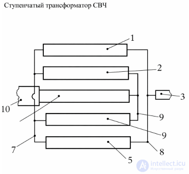
The invention is illustrated by a drawing, which shows, as an example, a schematic topology of a three-stage microwave transformer, where:
- 1, 2, 4, 5, 6 - quarter-wave coupled lines of the microwave transformer;
- 7, 8, 9 - jumpers providing the necessary electrical connections of the line sections;
- 3, 10 - input lines by means of which the microwave transformer is connected into the required characteristic impedance matching circuit.
Line 6 is the first high-impedance stage of the microwave transformer, which is electromagnetically coupled to lines 2 and 4, connected in parallel by means of jumpers 7 and 9, representing the second stage of the microwave transformer, and electromagnetically coupled to lines 1 and 5 of the third low-impedance stage of the transformer.
Jumpers 7 and 8 connect lines 1 and 5 of the low-impedance stage of the transformer in parallel.
Jumpers 9, 7, 8 provide the cascade connection of the microwave transformer stages.
The use of high-impedance lines 1, 2, 6, 4, 5, connected in parallel to achieve the required stage impedances of the transformer, leads to a reduction in the transverse dimensions of the microwave transformer, while the electromagnetic coupling of the stages leads to a reduction in the length of the transformer. In addition, the electromagnetic coupling of the stages leads to a broadening of the operating frequency band of the microwave transformer.
1. Input data
Given
For example
2. Equivalent circuit of the patent
The structure is a three-section transformer.
Each stage
is replaced by a system of coupled lines.
The equivalent looks like this
50 Ohm

│

┌────── λ/4 ──────┐
│                 │
│  first stage    │
└──────┬──────────┘
       │
══════════════════════ coupling

┌────── λ/4 ──────┐
│                 │
│  second stage   │
└──────┬──────────┘
       │
══════════════════════ coupling

┌────── λ/4 ──────┐
│                 │
│  third stage    │
└─────────────────┘

12.5 Ohm
3. ABCD matrix of a single quarter-wave line
Any line has
\theta=\beta lθ=βl
For a quarter wave
The matrix
4. Cascading of stages
The total matrix
After multiplication
A=0 D=0
From this the matching condition immediately follows
This is the first main equation.
5. Synthesis of impedances
For a binomial transformer
N=3
We use
we obtain
6. Transition to the patent structure
This is where the difference begins.
Each stage is replaced by several lines.
The equivalent impedance
If two lines are identical
If three lines
This is exactly why the author speaks of "high-impedance lines".
7. Electromagnetic coupling
Coupled lines are described by the even and odd modes.
Determined are
The mean impedance
The coupling coefficient
8. Matrix of coupled lines
For coupled lines
At
the matrix simplifies considerably.
After cascading, the new patent matrix is obtained.
9. Derivation of the coupling coefficient
From the condition
we obtain
After transformations
This is an approximate analytical formula.
10. Passband
From the matrix we obtain
We find
Then
After this, the operating band is determined
11. Length of the lines
12. Strip width
The Hammerstad formula is used
For
For large widths
the second formula is used.
13. Gap between coupled lines
Through
kk
is determined
SS
by the Cohn formulas.
Or by solving the inverse problem
14. Verification
The following are computed
- VSWR
- Return Loss
- Insertion Loss
- S11
- S21
- phase response
- group delay
15. Optimization
The last stage —
a slight adjustment
until maximum bandwidth is achieved.
Conclusion
The result is a complete engineering calculation, containing:
- the derivation of the ABCD matrices for each section and the entire structure;
- the synthesis of a three-stage transformer for the given impedances;
- the replacement of each stage with parallel coupled lines according to the patent scheme;
- the calculation of the even and odd characteristic impedances Z0e and Z0o;
- the determination of the electromagnetic coupling coefficients;
- the calculation of the length, width, and gaps of the microstrip lines;
- the computation of the S-parameters and the estimation of the passband.
For practical design, it is necessary to specify concrete initial parameters: ZS, ZL, f0, the permissible ripple (or the required reflection level), as well as the substrate parameters (εr, h, metallization thickness). After this, a complete numerical calculation of the structure with concrete dimensions can be performed.


Comments