
Lecture
Solid-state detectors use semiconductors to register X-ray radiation. Direct digital detectors are called so because they directly convert X-ray photons into electrical charge and, consequently, into a digital image. Indirect systems may have intermediate stages, for example first converting X-ray photons into visible light, and then into an electronic signal. Both systems generally use thin-film transistors to read out and convert the electronic signal into a digital image. Unlike film or CR, obtaining a digital image does not require manual scanning or development, so in this sense both systems are “direct”. Both types of systems have significantly higher quantum efficiency than CR.
In a digital imaging system, the incident X-ray image
must be sampled both spatially and in intensity
dimensions. In the spatial dimension, samples
are obtained as averaged intensity values over picture elements, or pixels. They are usually square in shape and
spaced at equal intervals across the entire image
plane. The fraction of a pixel that is sensitive to
the incoming signal is called the geometric fill factor. In
the intensity dimension, the signal is digitized into one
of a finite number of levels, or bits. The pixel size and
the number of bits must be chosen appropriately for the given
imaging task. Each pixel typically contains
a switching element and a readout/storage element.
Combining traditional materials for detecting X-ray radiation, such as
phosphors or photoconductors, with
a readout structure based on a large-area active matrix forms the basis of flat-panel X-ray detectors. Active matrix technology
offers a new, highly efficient method for electronically storing and measuring in real time the product
of X-ray interaction, regardless of whether that product
is visible-wavelength photons or electrical charges.
Three stages of image creation:
There are two types of digital flat-panel X-ray detectors (Fig. 1),
depending on the type of detection:
- Direct detection, involving a photoconductor, to create electrical charges upon detecting X-ray radiation,
- Indirect detection, involving a phosphor, to create visible photons upon detecting X-ray radiation.
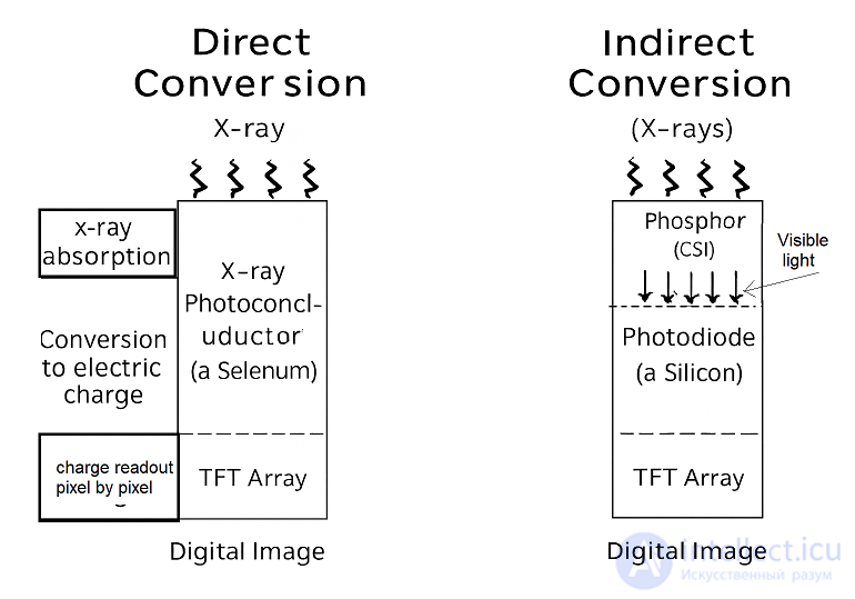
Fig. 1 – Direct and indirect conversion
Since the 1970s, semiconductor detectors based on silicon or germanium doped with lithium (Si(Li) or Ge(Li)) have been developed. X-ray photons are converted into electron-hole pairs in the semiconductor and collected to register X-rays. When the temperature is low enough (the detector is cooled by the Peltier effect or by even colder liquid nitrogen), the energy spectrum of X-rays can be determined directly; this method is called energy-dispersive X-ray spectroscopy (EDX or EDS); it is often used in small X-ray fluorescence spectrometers. Silicon drift detectors (SDD), manufactured using the traditional semiconductor fabrication process, provide cost-effective and high-resolution measurement of radiation power. ] Unlike conventional X-ray detectors such as Si(Li), they do not need to be cooled with liquid nitrogen. These detectors are rarely used for imaging and are effective only at low energies.
Practical application in medical imaging began in the early 2000s. [Amorphous selenium is used in commercial large-area, flat-panel X-ray detectors for mammography and general radiography due to its high spatial resolution and X-ray absorption properties. [ However, the low atomic number of selenium means that a thick layer is required to achieve sufficient sensitivity.
Cadmium telluride (CdTe) and its alloy with zinc, cadmium zinc telluride, are considered among the most promising semiconductor materials for detecting X-ray radiation because of their wide band gap and high atomic number, which allows operation at room temperature with high efficiency. Currently, methods such as bone densitometry and SPECT are applied, but flat-panel detectors suitable for radiographic imaging have not yet been manufactured. Research and development are currently focused on energy-resolving pixel detectors, such as the Medipix detector from CERN and the HEXITEC detector from the Science and Technology Facilities Council. [
Ordinary semiconductor diodes, such as PIN photodiodes or the 1N4007, will produce a small amount of current in photovoltaic mode if placed in an X-ray beam.
For direct conversion, a thick (~0.5–1 mm)
amorphous photoconductive layer of Se (a-Se) (Z = 34) is typically used. Pixels include a conductive
electrode for charge collection and a capacitor element for storing it. Interacting X-rays create charge in
the photoconductive layer, which is then distributed between
the intrinsic capacitance of the photoconductive layer and
the storage capacitance of the pixel (Fig. 2).
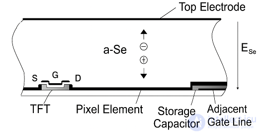
Fig. 2 – Cross-section of a single pixel with a-Se
In the band structure of the photoconductor, shown in
Fig. 3a, an optical photon with energy Eg can excite
an electron from the valence band into the conduction band,
leaving a hole in the valence band (internal photoelectric effect). The energy
of light photons is 1 to 3 eV, but the band gap Eg ~ 2
eV for photoconductors (Eg = 2.2 eV for a-Se). Otherwise,
Eg ~ 1 eV for semiconductors (e.g., 1.1 eV for Si).
For high-energy X-rays with energy
thousands of times higher than Eg, the rules
are different. Many materials used in
diagnostic imaging have a high atomic number Z, and
absorption of diagnostic X-rays is determined by
the photoelectric effect. A very energetic electron is released, which, as it passes through the material, causes
further ionization. Under these circumstances, the amount of energy required to create an electron-hole pair is not simply Eg, but 3Eg.
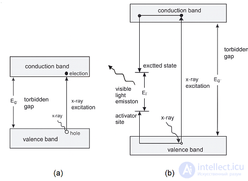
Fig. 3 – Electronic band structures of a) photoconductors and semiconductors, and b) a phosphor
Indirect detectors consist of a scintillator, which converts X-ray radiation into visible light that is read out by a TFT array. This can provide higher sensitivity compared with current direct detectors (based on amorphous selenium), although with a potential degradation in resolution. Indirect flat-panel detectors (FPDs) are widely used today in medicine, dentistry, veterinary medicine, and industry.
The TFT array consists of a sheet of glass coated with a thin layer of silicon in an amorphous, or disordered, state. On a microscopic scale, the silicon has been imprinted with millions of transistors arranged in a highly ordered array, similar to a grid on a sheet of graph paper. Each of these thin-film transistors (TFTs) is attached to a light-absorbing photodiode, forming a separate pixel (picture element). Photons striking the photodiode are converted into two electrical charge carriers, called electron-hole pairs. Since the number of charge carriers produced varies with the intensity of the incoming light photons, an electrical pattern is created that can be rapidly converted into voltage, and then into a digital signal that is interpreted by a computer to produce a digital image. Although silicon has outstanding electronic properties, it is not particularly good at absorbing X-ray photons. For this reason, X-rays first strike scintillators made of materials such as gadolinium oxysulfide or cesium iodide. The scintillator absorbs the X-rays and converts them into visible-light photons, which then strike the photodiode array.
In indirect conversion, the phosphor layer is
in close contact with the active matrix array (Fig. 4).
The intensity of light emitted from a given
area of the phosphor is a measure of the intensity of
the X-ray beam incident on the surface
of the detector at that point. Each pixel of the active matrix
has a photosensitive element that generates
an electrical charge whose magnitude is proportional to
the intensity of light emitted by the phosphor in
the area near the pixel. This charge is stored in
the pixel until the active matrix array is read out.
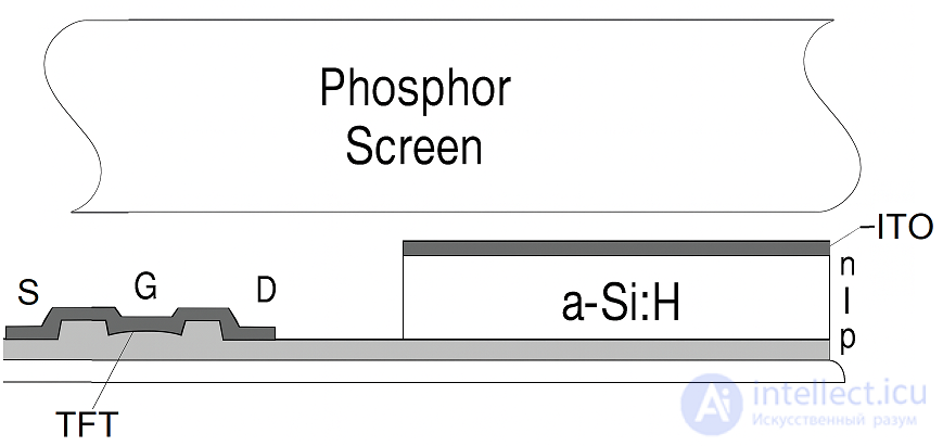
Fig. 4 – Cross-section of an individual pixel with a phosphor
The imaging system is completed with peripheral
circuitry that amplifies, digitizes, and synchronizes
image readout, as well as a computer that
processes and distributes the final image to
the appropriate electronic or print devices (Fig. 5).
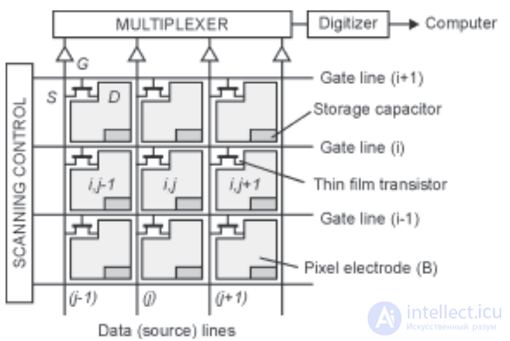
Fig. 5 – Arrangement of pixel groups on the active matrix

Training and material testing for explosive ordnance disposal (EOD). A 105 mm shell is X-rayed using a portable battery-powered X-ray generator and a flat-panel detector.
Digital radiography (DR) has existed in various forms (e.g., CCD and amorphous-silicon-based imaging devices) in the field of X-ray security inspection for more than 20 years and is steadily replacing the use of film for X-ray inspection in security and non-destructive testing (NDT) fields. DR has opened a window of opportunity for the security NDT industry thanks to several key advantages, including superior image quality, high probability of detection (POD), portability, environmental friendliness, and immediate image availability. [ 12 ]
Non-destructive testing of materials is critical in fields such as aerospace and electronics, where the integrity of materials is crucial for reasons of safety and cost. The advantages of digital technologies include the ability to provide results in real time.

Direct X-ray Imaging System (DXIS) — real-time display
| 1983 | Photostimulable phosphor radiography systems, first introduced into clinical practice by Fujifilm Medical Systems.] |
| 1987 | Digital radiography in dentistry was first introduced as “RadioVisioGraphy”. |
| 1995 | The French company Signet introduced the first dental digital panoramic system. |
| The first amorphous silicon and amorphous selenium detectors were introduced. | |
| 2001 | The first commercial indirect CsI FPD for mammography and general radiography appeared. |
| 2003 | Wireless CMOS detectors for dental work were first introduced by Schick Technologies |

Comments