
Lecture
Recall that this class includes those sensors in which, under the action of an external factor, the primary information signal arises in the form of an electric potential, a potential difference, or a voltage between certain points of an electric circuit. We will further classify voltaic sensors according to the physical nature of the factor under whose influence the electric potential, voltage, or electromotive force (EMF) arises and changes.
The use of thermocouples – electrically connected conductors made of two different materials – for measuring temperature is widely known. If the points of their electrical contact ("junctions") are at different temperatures, a potential difference arises between them, which is called the "thermo-EMF". Its physical cause is that in the region of the "hot" contact the charge carriers (electrons or "holes") have higher thermal-motion velocities. Therefore the diffusion flux of carriers from the "hot" junction to the "cold" one is greater than the diffusion flux from the "cold" junction to the "hot" one. In semiconductors this cause is further supplemented by the fact that the concentration of charge carriers near the "hot" junction is also noticeably higher. As a result, charge carriers accumulate near the "cold" junction, and a potential difference arises.
Over not too large temperature intervals the thermo-EMF in metal thermocouples is proportional to the temperature difference:
|
|
(6.1) |
In this expression  is called the thermo-EMF coefficient .
 and
and  – these are the temperatures of the "hot" and "cold" junctions respectively. For thermocouples made of metallic conductors, the values of the thermo-EMF coefficient lie within
  , while for semiconductors they can be even an order of magnitude higher.
From the magnitude of the thermo-EMF the temperature difference can always be determined unambiguously. The widest temperature measurement range (from – 270°C to 1300°C) is provided by the chromel/alumel thermocouple. The most commonly used thermocouples are copper/constantan, nichrome/constantan, iron/constantan, and so on. The role of one of the conductors can also be successfully played, for example, by doped silicon, which has a thermo-EMF coefficient even higher than that of metals.
To reduce their own heat capacity, thermocouples are made in wire or film form. Owing to its negligible thickness and mass, the measuring junction of a film thermocouple can have a very small heat capacity of its own and therefore a sufficiently small thermal inertia (less than 10 ms). Using a film thermocouple, one can measure the temperature even of very small bodies of millimetre and submillimetre size, to which it is glued.
Sometimes, in sensors that detect and measure light intensity, the photovoltaic effect is used – the appearance, under the action of incident light, of a potential difference between the illuminated and dark zones of a semiconductor. This is connected with the appearance in the semiconductor, upon absorption of photons, of additional electric charge carriers (internal photoelectric effect), which begin to migrate into the dark zone. The resulting photo-EMF is measured by electronic circuits with a very high internal resistance at the open-circuit terminals of the semiconductor. Owing to its very small inertia, it is used to monitor the power and shape of ultrashort laser radiation pulses.
The most commonly used type of voltaic sensors is the piezoelectric sensors. We have already mentioned their numerous applications when studying mechanical and acoustic sensors. Recall that the piezoelectric effect consists in the fact that mechanical deformation of a plate made of a piezoelectric material causes its additional polarization, as a result of which a potential difference arises between the electrodes deposited on opposite faces of the plate.
When designing and using piezoelectric sensors, two important circumstances must be taken into account. The first is that the surrounding medium always contains a certain amount of free ions, which, under the action of the potential difference, move and settle on the corresponding electrically charged surfaces of the piezoelectric material.
The electrical insulation of these surfaces from one another is never ideal, which is why, even if very small, leakage currents of charge arise. Therefore the potential difference between the two electrodes of the piezoelectric material, arising after its polarization or as a result of deformation, gradually decreases and after some time disappears. Because of this, piezoelectric sensors are sensitive only to deformations and forces that change with time, but cannot be used to measure long-acting forces and deformations. The second important circumstance is that the piezoelectric effect depends on temperature. This circumstance must necessarily be taken into account in sensors intended for precision measurements.
These difficulties can be circumvented by using the piezoelement in the mode of a piezoelectric resonator. The point is that not only the direct effect described above is always observed, but also the inverse piezoelectric effect: if a voltage is applied to the opposite electrodes of the piezoelement, the piezoelement deforms somewhat (contracts or stretches) in the transverse direction. When an alternating voltage is applied to the electrodes of the piezoelement, mechanical oscillations are excited in the piezoelement.
The amplitude of the forced mechanical oscillations depends not only on the amplitude of the applied alternating voltage, but also on its frequency. In the case where this frequency coincides with the frequency of the natural mechanical oscillations of the piezoelement, the so-called "electromechanical resonance" is observed: the amplitude of the excited mechanical oscillations increases sharply. Owing to the direct piezoelectric effect, the amplitude of the electrical oscillations also increases sharply in this case. For this reason, in alternating-current electrical circuits a piezoelectric resonator behaves as a high-Q resonant circuit with a Q factor of up to 10000. If, with the help of positive feedback and, for example, a transistor, synchronous pumping-in of energy is organized, then undamped electrical and mechanical oscillations at its own natural frequency arise and are sustained in the piezoelectric resonator.
A well-known type of voltaic sensors is also the so-called Hall-effect sensors. Their operation is based on the fact that the Lorentz force acts on electric charge carriers moving in a magnetic field. Therefore, if an electric current is passed through a plate of a conductor or semiconductor, then, in the presence of an external magnetic field, the electric charge carriers will be deflected by the Lorentz force in a direction perpendicular to the magnetic-field induction vector and to the direction of the current. As a result, a transverse potential difference arises, proportional to the current and to the magnitude of the magnetic-field induction.
Semiconductor diodes are formed, as is known, by means of local doping of a semiconductor, so that a so-called " -
- -junction" is formed – a transition layer between regions of the semiconductor of type
  and
and  .Electric current can freely flow through such a structure only in the "forward" direction – from the "anode" (the
  -type region) to the "cathode" (the
  -type region). The following theoretical expression is known, describing the current–voltage characteristic (CVC) of the diode, i.e. the dependence of the current flowing through it on the applied voltage:
|
|
(6.2) |
where  – the so-called "dark" current, caused by the thermal generation of charge carriers;
  – the electric charge of the electron;
  – the voltage applied to the diode;
  – Boltzmann's constant;
  – the absolute temperature of the diode.
From formula (6.2) it is clear that the current through the diode at a fixed voltage depends strongly on the absolute temperature. And if the passed current is fixed (for example, by means of a current-source circuit), the voltage on the forward-biased  -
- -junction increases almost linearly with rising temperature. Therefore semiconductor diodes and bipolar transistors are often used as sensing elements in temperature sensors. Such sensors are manufactured by many companies and provide temperature-measurement accuracy of up to ±0.1°C.
The best-known diode sensors are photodiodes. In photodetectors (light sensors) they behave as a light-controlled current source. Owing to the presence of an internal electric field in the depth of the  -junction, additional free charge carriers, which arise upon absorption of light quanta, begin to move and create an additional electric current proportional to the light intensity. It is called the "photocurrent". The dependence of the current through the photodiode on the voltage and the intensity of the incident light is fairly well described by the formula
|
|
(6.3) |
where  – the "dark" current;
  – the electric charge of the electron;
  – the voltage across the diode;
  – Boltzmann's constant;
  – the absolute temperature;
  – the quantum yield of charge carriers under excitation by light (the averaged number of carriers produced upon absorption of one light quantum);
  – the quantum intensity of the light flux (photons/s).
In practice, the light flux is often specified in lux. Then the coefficient in front of it has the meaning of the photodiode's light sensitivity and is given in µA/lx. The corresponding current–voltage characteristics of the photodiode in the absence of light  and at increasing intensities of it
  are shown on the left in Fig. 6.1.
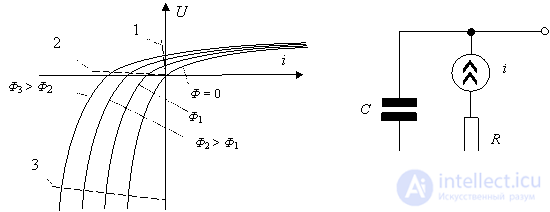
Fig. 6.1. Left – current–voltage characteristics of a photodiode at different illumination levels; right – equivalent electrical circuit of a photodiode
On the right of Fig. 6.1 the equivalent electrical circuit of the photodiode is given. Next to the current source, the intrinsic capacitance of the diode  and its internal resistance
  are shown. They largely determine the speed of the photodiode. To ensure high speed, one must, first of all, reduce the intrinsic capacitance of the photodiode. This is achieved by using photodiodes of
  structure, which are shown in Fig. 6.2. In such a structure, immediately next to the
  -region (the anode) of the diode, an extensive region of silicon, very much depleted of carriers and almost insulating (the so-called
  -region), is formed. This achieves a significant reduction in the intrinsic capacitance of the photodiode.
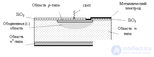
Fig. 6.2. Structure of a p-i-n photodiode
For a pair of charge carriers (an electron + a "hole") to form in a semiconductor upon absorption of a photon, the photon's energy must be greater than the width of the forbidden energy band.
For silicon, for example, this is 1.12 eV. Light quanta with a wavelength shorter than 1.1 µm have such energy – this is the so-called "red boundary" of photosensitivity for pure silicon. On the other hand, visible light with a wavelength substantially shorter than 0.1 µm is already strongly absorbed by silicon. Because of this, if the  -region of silicon is relatively thick, the light never reaches the
  -junction. Therefore, for silicon photodiodes to have high sensitivity in the visible region of the spectrum as well, the
  -region of silicon must be made very thin.
Photodiodes, which need to be sensitive to light from the near-infrared region of the spectrum with a wavelength from 1.2 to 2 µm, are made of germanium, while those sensitive to light of the mid- and far-infrared (IR) region are made from even more "narrow-gap" semiconductors  . Because of the narrow forbidden band, the dark current of such photodiodes and their shot noise at room temperature are too large. Therefore photodiodes that must operate in the mid- and far-IR region of the spectrum generally have to be cooled.
To provide sensitivity of silicon photodiodes also in the violet and ultraviolet regions, so-called Schottky photodiodes are used (Fig. 6.3). Instead of a  -junction, they form a so-called "Schottky barrier", arising at the "metal–semiconductor" interface. For this, a very thin layer of gold, sufficiently transparent to visible and ultraviolet light, is deposited by vacuum evaporation onto the photosensitive region of the silicon.
Ordinary silicon diodes have a forward voltage drop of about 0.6—0.7 volts; the use of Schottky diodes makes it possible to reduce this value to 0.2—0.4 volts.
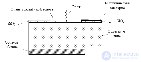
Fig. 6.3. Structure of a Schottky photodiode
Several modes of operation of photodiodes are distinguished. One of them – the photovoltaic mode (photo-EMF measurement mode), marked in Fig. 6.4 on the left by working section 1. The slope of this section is determined by the large internal resistance of the device or circuit measuring the voltage across the photodiode. Since the resistance is very high, only a very small current flows through the photodiode in this mode. Each value of the light flux  corresponds to its own measured voltage
  .
.
Much more often, photodiode light sensors use the electronic circuit shown in Fig. 6.4. One of the advantages of this circuit is that in it the voltage across the photodiode hardly changes, thanks to which the losses due to recharging of the input capacitance are minimized. With the help of an operational amplifier and a feedback resistor  the photocurrent is converted into an output voltage with substantial power gain. The working section of the photodiode in this mode, which is called the "photoelectric" mode, is represented on the left in Fig. 6.1 by segment 2. Its slope is determined by the rating of the feedback resistor
  . A feedback capacitance
  is introduced into the circuit (Fig. 6.4) to compensate for the phase shift and correct the sensor's frequency response].
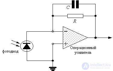
Fig. 6.4. Circuit for connecting a photodiode in the photoelectric mode
If maximum speed is required, the photodiode is used in the photoconductive mode, in which a large reverse bias voltage is applied to it. This leads to a significant expansion of the depletion region near the  -region and to a reduction in the intrinsic capacitance of the photodiode. However, it must be remembered that this also increases both the dark current and the intrinsic shot noise of the photodiode. A typical circuit for connecting a photodiode in this mode is shown in Fig. 6.4.
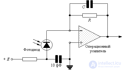
Fig. 6.5. Circuit for connecting a photodiode in the photoconductive mode
The corresponding working section is represented on the left in Fig. 6.1 by segment 3, the slope of which, as in the previous circuit, is determined by the rating of the feedback resistor  . If this rating is not too large, the voltage across the photodiode changes little. A photosensor built according to such a circuit can operate at frequencies of hundreds of megahertz.
Microelectronic technology has made it possible to form photodiodes on small silicon chips together with photocurrent amplification integrated circuits, providing not only high speed but also very high sensitivity.
Recall that a bipolar transistor consists of 2 adjacent  -junctions and has a structure of
  or
or  .
.
As a rule, a phototransistor has only 2 external leads – from the emitter and from the collector (a transistor with a "floating" base) and is connected into amplifying-measuring circuits in the same way as a photodiode. Owing to internal gain, phototransistors have a considerably better integral sensitivity to light. However, they are somewhat inferior to photodiodes in speed. Therefore they are preferred where light signals are very weak and maximum speed is not required, for example, in luminescent sensors.
Self-check questions 6
What are "voltaic" sensors? By what principle are they classified?
What is a "thermocouple"? What physical phenomenon underlies its operation?
What is a "piezoelement"? What physical phenomenon underlies its operation?
What is a "piezoelectric resonator"? Why can it be used as a force (pressure, deformation) sensor?
How does a Hall-effect sensor function?
Why can a semiconductor diode be used as a temperature sensor?
What is a "photodiode"? What does its spectral sensitivity depend on?
Name the main operating modes of photodiodes.
What is a "Schottky photodiode"? Where and for what are they used?
What are the advantages of phototransistors over the photodiode? And vice versa




Comments