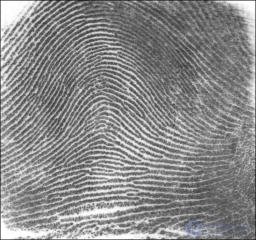
A fingerprint sensor is a biometric sensor that reads the unique pattern of friction ridges on a finger: ridges, valleys, bifurcations, ridge endings, pores and microscopic details.
When templates are built and compared after recognition, minutiae, or "Galton points", are used — the places in the skin's ridge pattern where individual ridges merge, split or break off, and which determine whether a fingerprint belongs to a given person. In other words, these are the points, unique to every fingerprint, at which the structure of the friction ridges changes.

1. General operating principle
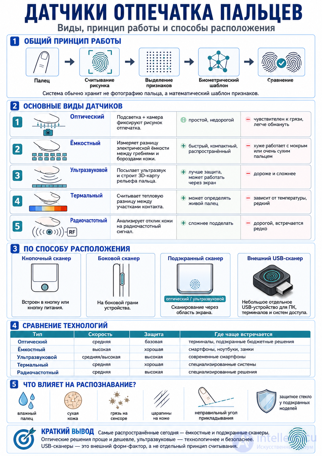
Every fingerprint scanner works along roughly the same lines:
Finger → pattern capture → digital image → feature extraction → template → comparison
That is, the system usually does not store a photograph of the finger but creates a mathematical template of features.
The main features are:
- ridge endings
- bifurcations
- bends
- islands
- deltas
- pattern cores
- distances between points
Main types of fingerprint sensors
There are many physical operating principles behind fingerprint scanning sensors, for example:
- An optical sensor sees the fingerprint the way a camera does.
- A capacitive sensor measures the electrical relief of the skin.
- An ultrasonic sensor builds a three-dimensional map of the finger using sound.
- A thermal sensor reads the heat trace.
- A radio-frequency sensor analyzes the response of the tissue to a radio signal.
The most widespread today are capacitive and ultrasonic sensors, while under-display smartphones more often use optical and ultrasonic scanners.
1. Optical sensor
This is one of the oldest and most straightforward types.
How it works
It works almost like a small camera.
The finger is placed on the glass
↓
A light source illuminates the skin
↓
The camera records the pattern
↓
An algorithm analyzes the light and dark lines
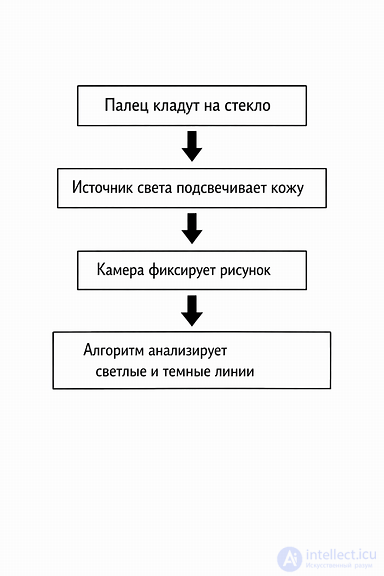
The ridges of the finger, being closer to the glass, reflect light differently than the valleys do. This is how the fingerprint image is obtained.
Single-prism recognition method
In 1971, optical fingerprint capture devices began to acquire images by scanning the print left on the surface of the finger — a process prone to interference. Various designs of optical fingerprint sensors appeared subsequently. Early optical fingerprint scanners usually required a separate light source and a prism. Figure 3a shows the typical total-reflection principle, and this total-reflection identification method is affected by finger moisture and creases. Figure 3b shows an imaging device placed beyond the critical angle, where only light reflected from the ridge beyond the critical angle reaches the imaging device. Figure 3c uses the method of dispersion inside the finger, in which the light source penetrates into the finger, is scattered and passes through the fingerprint layer, reaching the transparent plate of the sensor, and must have a refractive index close to that of human tissue. Figure 3d shows a multispectral light source for detecting fingerprint images both on the surface and inside the print. Because the transmission properties of biological tissue depend on wavelength, different wavelengths penetrate to different depths, which requires several light sources and two polarizers in this sensor. In 2016, Baek created a fingerprint sensor based on a modification of the optical path that makes it possible to detect wet fingerprints. Because the sensor uses numerous optical components, its size is considerable. The need for minimal dimensions led to the development of line-scanning sensors, which are suitable both for integration into mobile devices and for acquiring large fingerprint images. Most line-scanning sensors are swipe sensors, which introduce degrees of freedom as a result of variation in swipe speed and direction. Existing swipe fingerprint sensors can be divided into capacitive and optical ones. The optical type has a smaller size (4 × 0.9 mm²) and a higher resolution (1000(H) 625(V)), consists of an optical bonding layer with the same refractive index as the overlaid glass, and has a single swipe direction
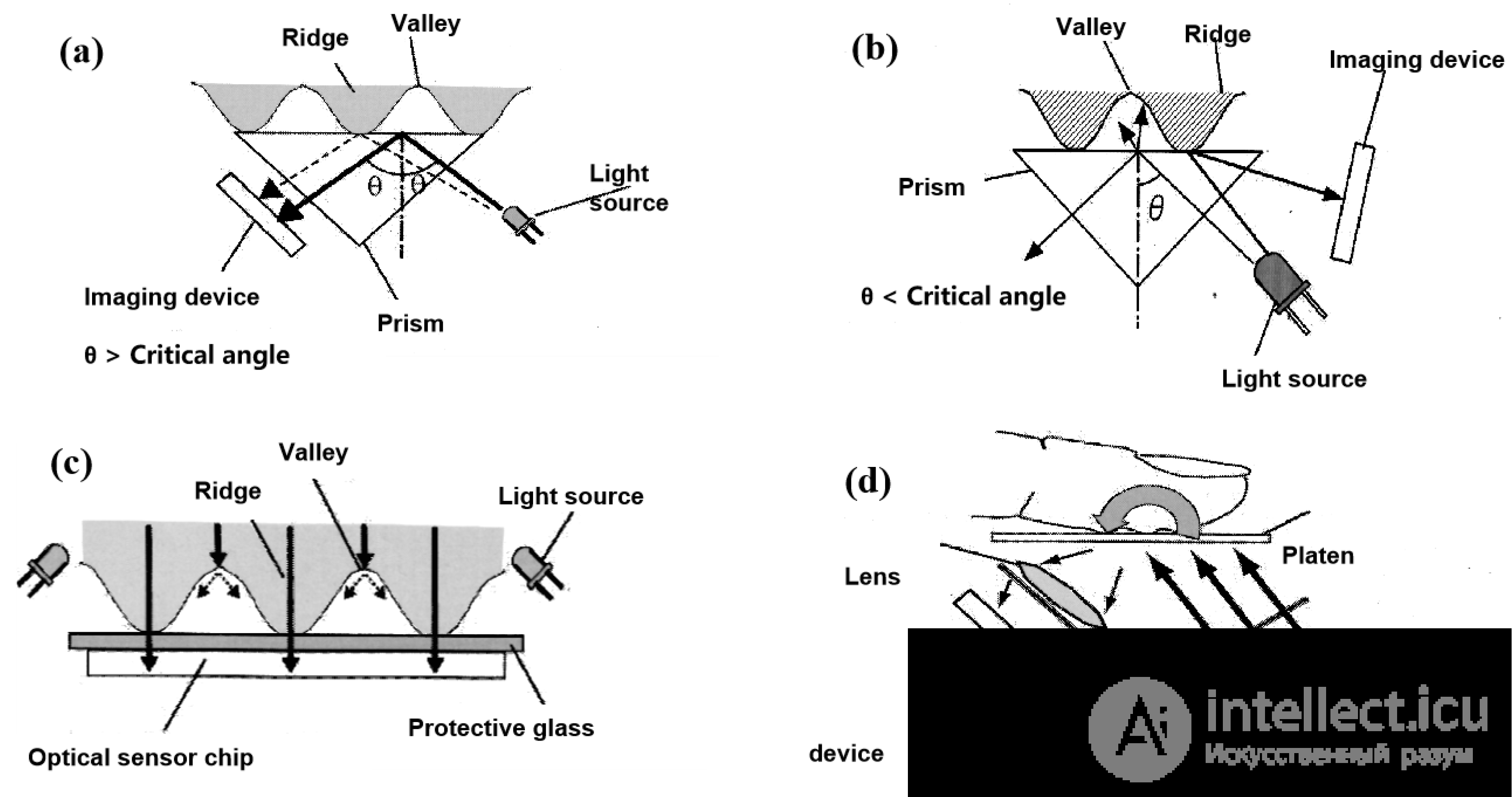
Figure 3. Various designs of optical fingerprint sensors. ( a ) Principle of the total internal reflection method; ( b ) principle of the light-path separation method; ( c ) principle of the light dispersion inside the finger method; ( d ) principle of the multispectral method
. Identification method using TFT technology
Thin-film transistors (TFTs) have been under development for more than 40 years, replacing traditional semiconductor sensors with photosensitive TFT panels. In 1961, Weimer created the first thin-film transistor (TFT) [ 94 ]. Using amorphous silicon (a-Si:H) as the active layer, Street created a TFT device in 1979, and it was found that amorphous thin-film transistors (a-Si TFTs) could be used as switching devices for active-matrix liquid crystal displays (AMLCDs) [ 95 ]. TFTs are produced by magnetron sputtering and chemical deposition on non-single-crystal substrates such as glass or plastic plates, and large-scale semiconductor integrated circuits (LSICs) are produced by processing films. A standard TFT-based optical sensor device consists of a grid of pixels on glass and an operational amplifier (OPAMP) in an external readout integrated circuit (IC) [ 96 ]. This method can be used to create large-scale sensor arrays using optical fingerprint sensors. Table 2 lists the specific parameters for the four main types of TFT technology: non-crystalline silicon TFT, polycrystalline silicon TFT, organic TFT and amorphous oxide TFT.
Table 2. Different types of TFT.
Semiconductor
materials |
Process
temperature/°C |
Mobility/ cm² ∙ V⁻¹ ∙ s⁻¹ |
Number of
lithography steps |
Capacity |
| Amorphous silicon |
<350 |
0.1–1 |
4–6 |
high |
| Polysilicon |
<700 |
10–400 |
5–11 |
low |
| Organic materials |
<150 |
<2 |
- |
low |
| Amorphous oxide |
<350 |
1–100 |
4–7 |
high |
3.2.1. Based on amorphous silicon thin-film transistor (TFT) technology.
Thin-film transistors (TFTs) based on hydrogenated amorphous silicon (a-Si:H) are the predominant thin-film transistor technology used in flat panel displays today [ 97 ]. A-Si:H TFTs offer the advantages of a low process temperature (<350 °C), good uniformity over large areas, low cost and low leakage current; at present they are the predominant technology for commercial LCDs. However, the field-effect electron mobility of a-Si:H TFTs is only 0.4–1.5 cm² / (V·s), and the field-effect hole mobility is considerably lower, which prevents their use in high-definition and current-driven displays. In addition, the low mobility of a-Si:H TFTs is compensated for by increasing the channel width in order to obtain sufficient drive current. However, larger a-Si:H TFT devices reduce the transparency, resolution and brightness of the display [ 98 ].
The absorption spectra and quantum efficiency of a-Si:H and Si have been compared. In the 0.4–0.75 µm range the material absorbs more light than the Si layer, but the Si layer absorbs more light at longer wavelengths (>0.75 m) than the a-Si:H film does. In visible light an a-Si:H diode generates a larger photocurrent than an Si diode, and a-Si:H p-n diodes have a higher output quantum efficiency than Si p+/n diodes over most of the visible spectrum [ 99 ].
Based on amorphous silicon TFT technology, optical fingerprint sensors can achieve thinness, compactness and a large area [ 100 ]. The PPS structure makes it possible to create A-Si:H field-effect transistors [ 101 ]. Thin optical type (TOT), hidden optical type (HOT) and hidden under display (HUD) fingerprint sensors based on hydrogenated amorphous silicon are already available for mass production [ 99 ]. Sensor sizes range from tiny (4.0 mm × 8.0 mm) for identifying a smartphone user up to four-finger size (3.2″ × 3.0″) for public security service verification. Table 3 and Figure 4 present a comparison of the three types of fingerprint sensor.
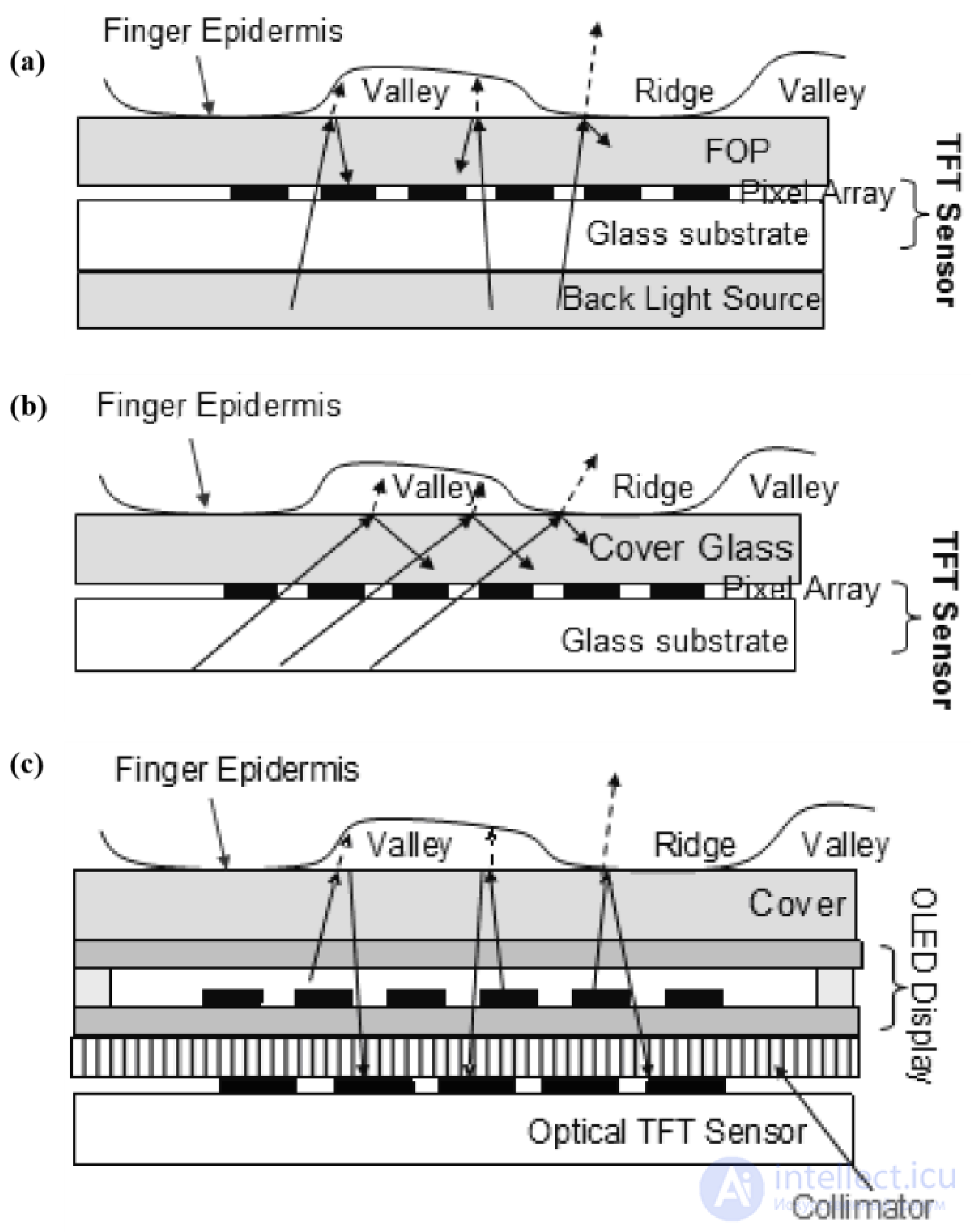
Figure 4. ( a ) TOT structure, ( b ) HOT structure and ( c ) HUD structure [ 99 ].
Table 3. TOT, HOT and HUD structures.
| Sensor type |
TOT |
HOT |
HUD |
| Light source |
460 nm LED |
Invisible LED at a specific wavelength |
OLED |
| light source position |
Back side of the TFT sensor |
Under the TFT glass substrate |
- |
| Sensing area |
FAP10(0.5″ × 0.65″)~FAP60(3.2″ × 3.0″) |
10 mm × 14 mm |
12 mm × 20 mm
12 mm × 40 mm
40 mm × 51 mm |
| bonding method |
Optical adhesives |
Optically clear resin (OCR)
Optically clear adhesive (OCA) |
- |
| Fiber optic plate |
√ |
- |
- |
| Collimator |
- |
- |
√ |
| Sensor top |
Fiber optic plate |
Glass plate |
OLED |
3.2.2. Based on polycrystalline silicon thin-film transistor (TFT) technology.
Low-temperature polycrystalline silicon (LTPS) technology refers to a method of producing high-quality polycrystalline silicon films and thin-film transistors (TFTs) at temperatures below 600 °C [ 102 ]. The pixel array and the driver circuitry of a polysilicon TFT-LCD can be combined on the same glass substrate in order to integrate the peripheral driver and the display. Compared with a-Si:H TFTs, LTPS TFTs offer the advantages of high mobility (often two orders of magnitude higher) and a large drive current, as well as reduced power consumption and a smaller device area; they also solve the high-density problem, improving yield and lowering production costs [ 103 ]. In addition, p-Si is resistant to optical interference, and the leakage current does not increase under illumination, which makes a light-shielding layer unnecessary. It is possible to build a high-definition system on panel (SOP) that combines the display array and the peripheral drivers, significantly increasing the reliability of the system. LTPS TFTs have already replaced OLED displays in miniature commercial screens.
As amorphous silicon thin-film transistors move toward high capacity, high brightness and high resolution, LTPS technology compensates for the smaller pixel size and the shorter pixel charging time, and also solves the problems associated with the difficulty of forming high-density conductors and integrating the display area with the surrounding driver circuitry [ 104 ]. There are two ways of obtaining polycrystalline silicon films: direct and indirect methods. Direct methods include low-pressure chemical vapor deposition (LPCVD) [ 105 ] and catalytic chemical vapor deposition (cat-CVD) [ 106 ], while indirect methods use recrystallization of amorphous silicon films, the crystallization techniques for which mainly include solid phase crystallization (SPC) [ 107 ], rapid thermal annealing (RTA) [ 108 ], metal-induced lateral crystallization (MILC) [ 109 ], microwave crystallization [ 110 ] and laser crystallization (LC).
A new photosensitive material is used as the sensing material. The metal/sensing material/ITO sensor structure is integrated into the LTPS TFT process [ 111 , 112 , 113 ]. Using an active pixel sensor (APS) circuit, an optical in-cell fingerprint sensor (iFP) technology is created that combines display, touch control and FPS capabilities [ 114 ]. Meanwhile, amorphous silicon can be placed above the polysilicon in a manner similar to Figure 5 in order to create a vertical hybrid PIN photodiode (HPAS-PIN) [ 115 ]. Fingerprints that can be effectively acquired with this optical image sensor array are shown in Figure 6a. However, this array cannot capture a fingerprint image in the presence of a color filter. An LTPS image sensor (LIS) can operate using an active pixel sensor (APS) circuit based on an LTPS substrate [ 116 ], shown in Figure 6c. An LTPS-TFT LCD has been developed with a resolution of 400 PPI, touch and on-screen fingerprint scanning capability, able to capture a fingerprint image even when the finger is 1.0 mm above the LIS array, with a fingerprint scanning area resolution of 256 × 256 and a sensor with increased sensitivity and noise immunity.
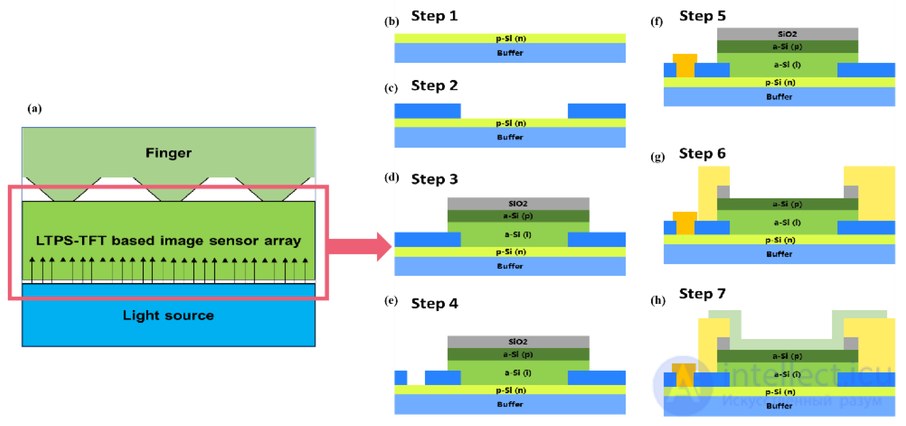
Figure 5. ( a ) Structure of the optical image sensor array and the fingerprint image obtained with it. ( b ) A 300 nm silicon oxide buffer layer and a 50 nm intrinsic amorphous silicon (a-Si) layer are deposited in sequence, after which the a-Si is converted into p-Si by excimer laser annealing. Phosphorus ions are then introduced into the p-Si to form a p-Si layer with N+ ions. ( c ) A 230 nm insulating layer is deposited and the first via pattern, 20 × 10 µm in size, is formed by photolithography and dry etching. ( d ) A 600 nm intrinsic amorphous silicon layer and a 50 nm silicon oxide layer are deposited on the first via layer and the insulating layer, after which boron ions are implanted into the surface of the intrinsic amorphous silicon layer, converting part of the upper intrinsic amorphous silicon layer into a p-Si layer with P+ ions. Because the ion concentration distribution is Gaussian in shape, there is no sharp boundary between the P+ amorphous silicon (a-Si) and the intrinsic amorphous silicon (a-Si). At this stage the intrinsic amorphous silicon in the first via contacts the N+ p-Si together with the upper P+ a-Si layer, forming a hybrid PIN photodiode of p-Si and a-Si. After that the amorphous silicon is patterned into an island 25 × 15 µm in size by photolithography and dry etching. ( e ) A second via is formed in the insulating layer next to the first via using the same photolithography and dry etching. ( f ) A metal layer is deposited on the second via, serving as the cathode contact of the photodiode. ( g ) An organic planarization layer is deposited and a third via is formed above the first one. At this stage the silicon oxide is removed in order to expose the P+ a-Si surface at the same time. ( h ) Deposit a transparent conductive ITO layer, which will serve as the anode contact of the photodiode [ 115 ].
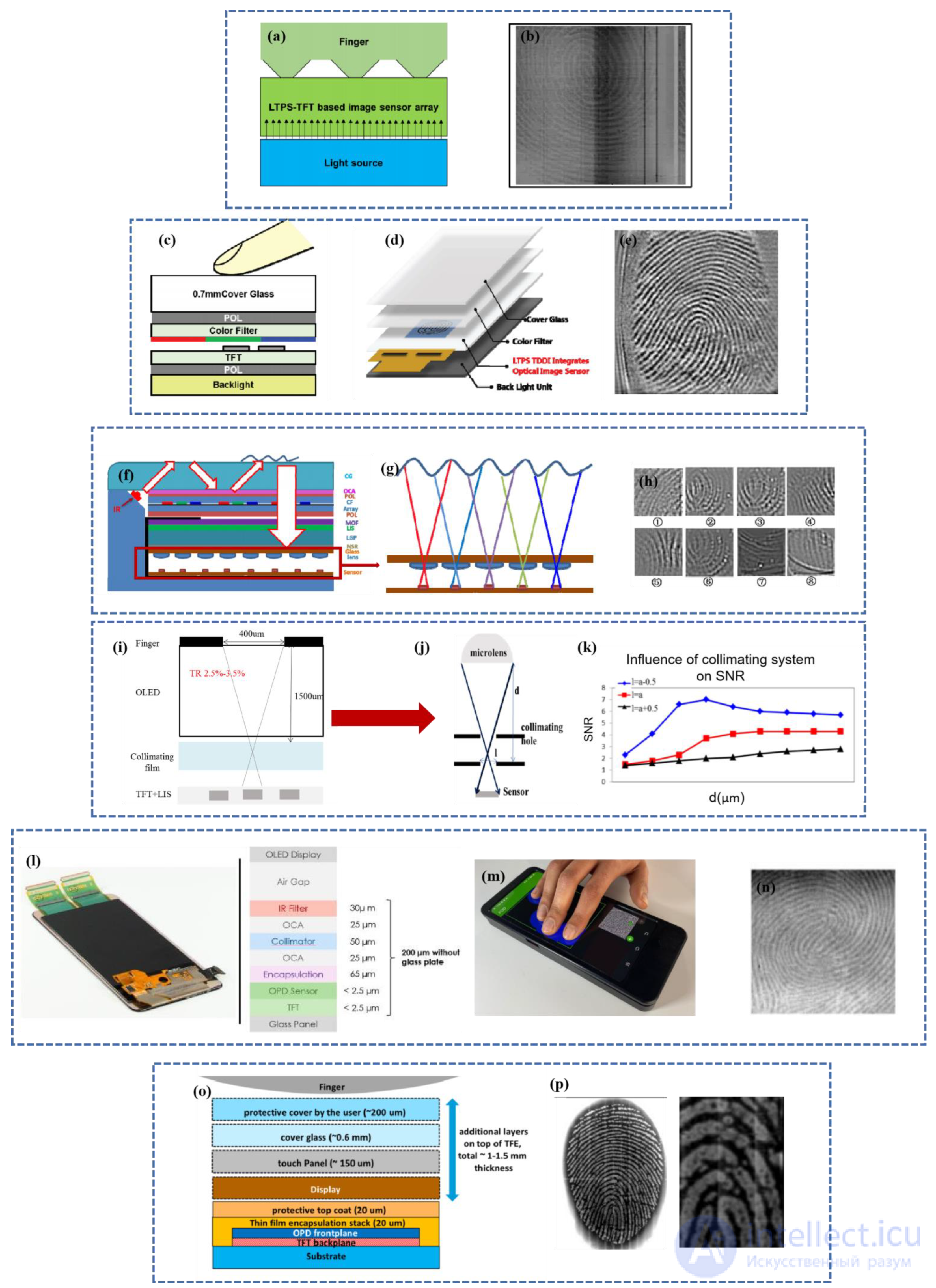
Figure 6 (a) Structure of an optical image sensor array and (b) the fingerprint image captured with it; (c) cross-shaped structure of an in-cell fingerprint sensor. (d) Structure of an LCD with an in-cell fingerprint sensor; (e) fingerprint image. (f) Field-of-view diagram of a microlens array, (g) collimating optical path based on a microlens array, (h) the fingerprint image captured with it, (i) multilayer structure of an under-OLED fingerprint sensor and (j) diagram of a collimating system on a photosensor. (k) Effect of the collimating system on the signal-to-noise ratio and (l) fingerprint on display (FoD module). Assembly of the multilayer structure of the FoD module, (m) design of an organic image sensor, (n) fingerprint capture with it, (o) structure of the fingerprint sensor and (p) fingerprint capture with it.
When an LCD is used as the light source, the panel and its opaque backlight obstruct the passage of visible light, and an air gap inevitably forms between the LCD and the backlight. An optical image sensor array can be built into an LCD, using either the backlight or an additional LED as the light source, with the image sensor array placed on a TFT substrate, which eliminates the backlight as the light source. It is also possible to place an IR image sensor and an IR light source beneath the backlight, in which case the IR radiation from the IR source passes through the LCD module and is received by the IR image sensor after reflection off the fingerprint.
Ye [ 117 ] proposed a collimating optical path based on a microlens array with a 940 nm IR light source located beneath the bottom plate of the cover glass. By adjusting the exit angle and the emission angle of the light source, total reflection of all obliquely incident light at the upper and lower surfaces of the CG can be achieved. As shown in Figure 6 f,g,h, the beam carrying the fingerprint information passes successively through each film layer before being captured by the sensor array under the display. Because of the sensor size, this lens block has to be confined to a tiny area.
A comparison of light detection in an LCD with under-screen detection and light detection in an OLED display: OLED uses self-emissive radiation as the light source and employs microcollimators to prevent the light signals from overlapping. Thanks to the under-screen design and the self-emissive properties, the depth-to-width ratio of the microcollimator aperture can be chosen freely to achieve adequate collimation without letting an excessive amount of scattered light reach the CIS.
In addition, researchers have developed optical fingerprint recognition [ 118 ] that can be integrated into LTPS imaging display technology beneath an OLED display and can cover every display size. OLED uses its own self-emissive light as the light source and employs microcollimators to prevent the light signals from overlapping. The signal variation coefficient is improved by 50 percent through refinements to the process and the circuit architecture. Thanks to the improved collimation technology, the signal-to-noise ratio is practically doubled.
As shown in the illustration, the collimating system consists of a collimating aperture and a microlens. One approach places the collimating system above the photosensor, as shown in Figure 6 f,g, while another method prepares the collimating system directly above the photosensor, as shown in Figure 6 i,j,k, which presents the signal-to-noise ratio (SNR) result for the collimating system. The collimating system comprises a collimating aperture and a microlens. The light-receiving capability of the sensor can be improved by exposure followed by immediate alignment of the sensor's collimating mechanism.
3.2.3. Oxide TFT-based technology
Thin-film transistors (MOS TFTs): thanks to the advantages of good uniformity, high mobility and strong process compatibility with a-Si TFTs, the following performance aspects are commonly considered in metal-oxide TFT line driver circuits: speed [ 121 ], power consumption [ 122 ] and reliability [ 123 , 124 ].
Conventional amorphous silicon (a-Si:H) TFTs and low-temperature polycrystalline silicon (LTPS) TFTs have proved difficult to apply to the demand for flat panel displays of enormous size and high resolution. The semiconductor industry has reached an era in which material limitations constrain device dimensions. Since 2003, transparent TFTs made from amorphous oxide semiconductors have been at the center of worldwide research [125 ] . Compared with silicon materials, oxide semiconductor films, exemplified by a-IGZO, offer a superior low processing temperature, a long service life, high transmittance, a wide bandgap (transparency) and high carrier mobility [ 126 , 127 , 128 , 129 , 130 ], and they are widely used in liquid crystal displays, memory [ 131 , 132 ] and the Internet of Things [ 133 ]. AOS TFTs are therefore expected to replace a-Si:H TFTs as the core devices of the next generation of flat panel displays (flexible displays, transparent displays, etc.).
Qin [ 134 ] presented a near-infrared optical fingerprint sensor based on a passive pixel sensor (PPS) array and oxide (IGZO) TFT technology. This optical sensor uses an organic photodiode (OPD) as its sensing element. This organic-inorganic hybrid thin-film photodetector is able to obtain a clear fingerprint image. In addition, a flexible fingerprint sensor built on a polyimide substrate was created. Because of the high penetration of near-infrared light, part of it can pass through the finger and reach the sensing element when the finger touches the sensor surface. Moreover, the ridges and valleys of the fingerprint represent different optical paths. In a ridge area, part of the near-infrared light is reflected from the surface and the remaining light falls on the detecting pixel. In a valley area, only part of the near-infrared light passes into the air and subsequently reaches the detecting pixel. Because of the ridge and valley areas of the fingerprint, different amounts of light arrive at the surface of the sensor pixel. Fingerprint recognition is performed in this way. Each pixel measures 50.8 µm, which is equivalent to a resolution of 500 PPI.
3.2.4. Organic TFT
The transition from TFTs to OTFTs is not straightforward. It is generally accepted that Heilmeier [ 135 ] discovered the OTFT field-effect phenomenon in a thin film of copper phthalocyanine. In 1986, Tsumura invented the first organic thin-film transistor by electrochemically synthesizing polythiophene and using it as the core material of the OTFT; the resulting mobility, however, was only 10⁻⁵ cm² / (V·s) [ 136 ]. On the other hand, thanks to the good flexibility, low cost and characteristics of organic materials themselves, various institutions have at different times carried out in-depth studies of thin-film morphology and of the methods used to produce such films, and applications in the field of display devices will become ever more widespread and significant.
Optical fingerprint biometrics based on organic photodiode (OPD) technology [ 119 ] can be built in under a smartphone display to provide full coverage and to capture up to four fingerprints [ 120 ]. As shown in Figure 6o , the full-screen optical fingerprint module is easily integrated into mobile devices (attached to the OLED panel or with an air gap). It effectively prevents spoofing under visible light (540 nm) and near-infrared light (850 nm and 940 nm). Figure 6l shows that an Android application was created for this purpose, allowing the user to enroll and verify a fingerprint with a matching time of less than 500 ms and a high-contrast image resolution of 5 Cy/mm.
Faced with the difficulties of full-screen TFT technology, Tai [ 137 ] chose a gap TFT as the optical system of the array in Figure 6n . For fingerprint recognition applications, the high photocurrent of the gap TFT results in a large signal and fast readout, which is a substantial advantage. A collimator is placed between the OLED screen and the gap TFT sensor array. Algorithms are used to remove the background and enhance the fingerprint image. The ridges and valleys of the fingerprint are clearly visible.
3.3. Identification method using optical coherence layer scanning technology
Modern civilization shows great interest in developing fingerprint recognition systems with a high degree of security and robustness in the fingerprint identification process. The ability of optical coherence tomography (OCT) to obtain depth information about the layers of the skin [ 16 ] has created a new field of research in fingerprint recognition [ 138 , 139 ]. OCT was initially introduced into the field of fingerprint recognition for anti-spoofing [ 140 ], including automatic spoof and real-time detection [ 141 , 142 , 143 , 144 , 145 , 146 ], reconstruction of internal fingerprints (i.e., subcutaneous prints corresponding to the living epidermis) [ 147 , 148 , 149 , 150 , 151 , 152 ] and fingerprint identification/recognition [ 153 , 154 , 155 , 156 ]. At present, confocal scanning OCT provides the greatest imaging depth, but it is considerably more expensive because it requires additional components such as lasers. Using an inexpensive light source, for example a light-emitting diode (LED) or a thermal source, makes it possible to perform full-field optical coherence tomography (FF-OCT), a variant of OCT. Unlike typical confocal scanning OCT, FF-OCT uses a camera with practically instantaneous access to the fingerprint and step-by-step image scanning to acquire axial images. The absence of pinholes in the detection path used in confocal OCT and the shallow imaging depth are drawbacks of FF-OCT. FF-OCT has nevertheless proved effective in a variety of biological applications, including imaging of the skin, brain tissue, the walls of the gastrointestinal tract and the cornea.
Imaging methods based on optical coherence layers take into account the effects of moisture, wrinkles and the absence of contact. Exploiting the varying transmittance of ridges and valleys, a red LED illuminates the nail side of the finger, forming a fingerprint image [ 87 ]. FF-OCT can also use a Michelson interferometer and a silicon camera [ 157 ]. It includes a small, lightweight LINOS opto-mechanical system covered by a plexiglass panel measuring 30 cm × 30 cm × 1 cm. The sensor produces images measuring 1.7 cm × 1.7 cm with a spatial sampling frequency of 2116 dots per inch (dpi). The fingerprint is an external image obtained at a distance of 15 m. The image displayed in the 33–103 µm range represents the cuticle, and the sweat glands appear as white dots. The photographs presented in the 121–210 µm range correspond to the living epidermis. The images at a depth of 121–156 µm represent the ridges of the internal fingerprint, whereas the images from a depth of 191–210 µm represent the valleys, which makes it possible to obtain fingerprint images [ 158 ]. Figure 7 shows scan images of normal fingerprints, wet fingerprints and fingerprints based on the optical coherence layer.
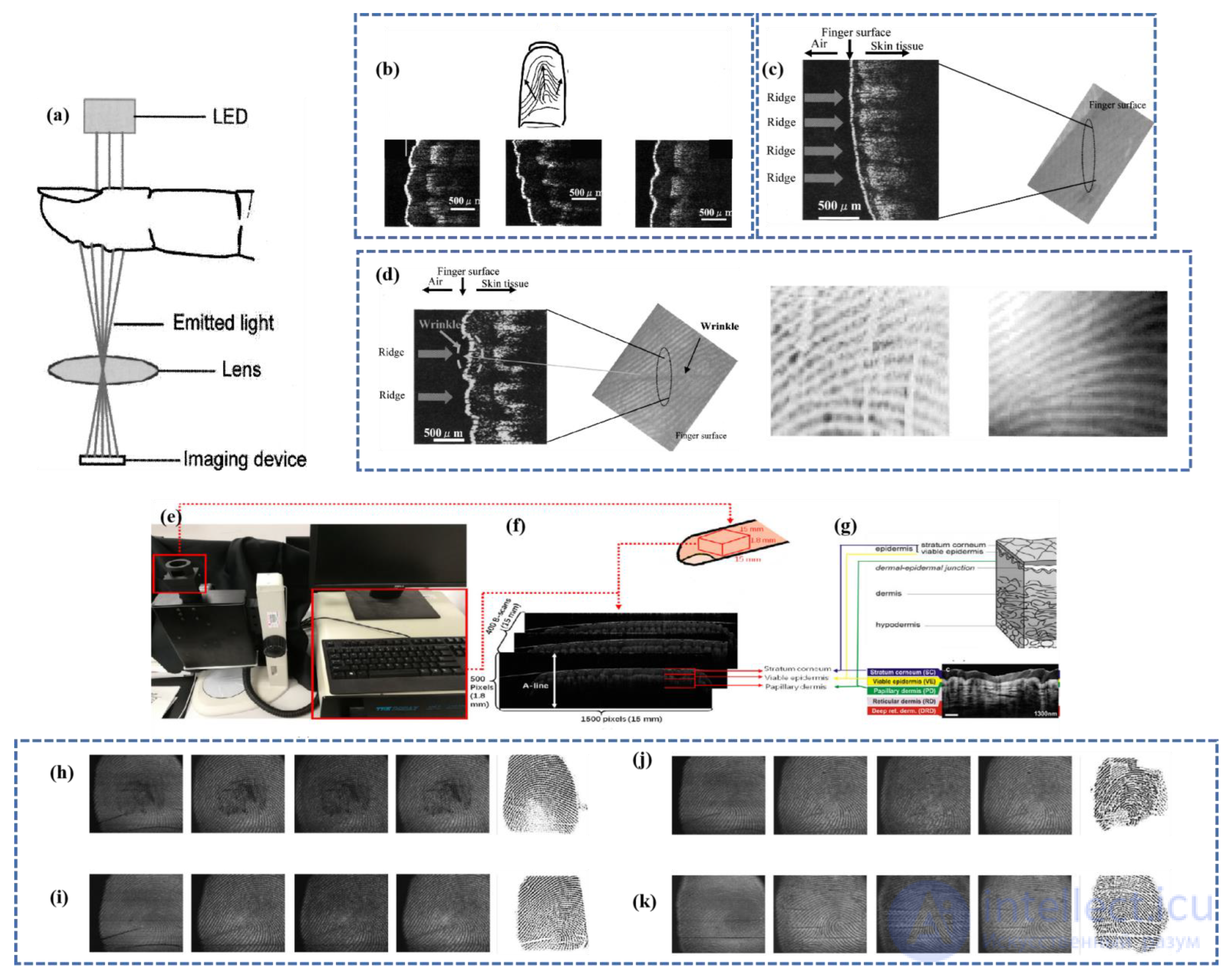
Figure 7. ( a ) Design of a new fingerprint sensor using scattered transmitted light. ( b ) A normal fingerprint and OCT images. ( c ) Fingerprint images of a wrinkled finger and an OCT image. ( d ) An image of an almost flat finger and an optical coherence tomography (OCT) image [ 89 ]. ( e ) Design of the equipment, ( f ) structure of subsurface fingerprints, ( g ) the various layers of subsurface fingerprints and ( d - k ) various fingerprint images. From left to right, the images correspond to the stratum corneum, internal, papillary, fused and traditional 2D fingerprints [ 159 ].
Liu [ 159 ] proposed a fingerprint identification system based on optical coherence tomography (OCT), shown in Figure 7 e–g. This device uses an SD-OCT approach with a light source whose central wavelength is 840 nm; the source light is generated by a superluminescent diode (SLED), and two identical telephoto lenses serve as the focusing and the scanning lens, respectively [ 160 ]. The device is designed for touch-based print capture. When capturing a fingerprint, the finger has to be placed on a fixed cover glass. In contactless OCT, the use of a fixed cover glass eliminates the depth-dependent roll-off problem. The axial and lateral resolution of the SD-OCT device is 8 µm and 12 µm, respectively. The apparatus records an image measuring 15 mm × 15 mm with an average speckle size of 24 µm. Each scan captures a fingertip volume of 1.8 mm × 15 mm × 15 mm with a spatial resolution of 500 × 1500 × 400 pixels.
Where it is used
Used in:
- office scanners
- access control systems
- older biometric terminals
- some laptops
Pros
- simple technology
- inexpensive
- can produce a good image
Cons
- easier to spoof with a photograph or a dummy finger
- works poorly with dirty/wet fingers
- requires a separate optical module
- takes up more space
2. Capacitive sensor
This is the most common type in smartphones, buttons and laptops.
How it works
It measures the difference in electrical capacitance between areas of the skin and the sensor array.
A skin ridge is closer to the sensor → higher capacitance
A furrow is farther from the sensor → lower capacitance
The result is a map of the fingerprint.
finger
↓
[sensor array]
↓
map of electrical differences
↓
digital template
As semiconductor [ 161 ] technology advanced and authentication devices had to be packaged compactly and cheaply into mobile devices such as smartphones and integrated circuits, capacitive fingerprint sensors appeared. In principle, capacitive and inductive fingerprint sensors share a common "flat" plate carrying hundreds of integrated semiconductor devices and a surface layer that is typically a few microns thick. The unevenness of the fingerprint, that is, the actual distance between a ridge and the ridge touching the plate, changes when a finger is placed on the surface of a capacitive sensor, which results in different capacitance values [ 162 , 163 ]. The capacitance values are converted into current or voltage values, which are then converted into operator data by an ADC. The higher the contrast of the fingerprint, the closer the fingertip is to the surface. The device completes the fingerprint capture process by averaging the results obtained.
An under-display optical fingerprint sensor uses the difference in light reflection from the ridges and valleys of a finger to recognize fingerprints, but it has difficulty reading dry fingers, which do not make regular, continuous contact with the protective layer of the sensor [ 86 , 164 ]. In terms of identification time, dry-finger recognition and manufacturing yield, under-display ultrasonic fingerprint sensors have room to develop. Unlike them, optical and ultrasonic on-screen sensors are compatible exclusively with OLED panels. A reverse capacitive system can operate on the screen. Authenticity can be determined by detecting the impedance of a fingerprint, which has different impedance frequencies [ 165 ] and different amounts of eddy current due to the turbo-impedance effect [ 166 ], as well as by using a temperature sensor [ 167 ]. Capacitive fingerprint sensors still need considerable improvement in fingerprint detection.
Ridge width ranges from 100 m to 400 m, valley depth from 60 µm to 220 µm, and valley width from 75 µm to 200 µm [ 157 , 168 ]. When a ridge and a valley are adjacent electrodes, the difference in mutual capacitance can exceed 400 aF [ 169 ]. Thanks to charge sharing [ 92 ], charge transfer, capacitive feedback [ 170 ] and sample-and-hold circuits, capacitive sensors [ 171 ] can detect weak signals.
4.1. Self-capacitance fingerprint sensor
In a self-capacitance fingerprint sensor, the capacitance between the sensing pin and the power supply is monitored. When a finger is applied to the sensor, its capacitance increases and the measured voltage rises and changes, which makes it possible to detect finger contact. In self-capacitance sensing, the unit cell usually consists of a sensor circuit based on silicon technology [ 92 , 165 , 172 ], and the sensor capacitance can be measured and detected directly and independently. Silicon fingerprint sensors can be fabricated only on opaque, brittle and non-flexible silicon wafers and can therefore be implemented only in rigid devices such as smartphone buttons. Self-capacitance is incompatible with multi-touch functionality.
In the self-capacitance measurement approach, the cell usually includes a silicon-based sensing plate and a readout circuit [ 165 , 173 ]. High sensitivity can be achieved thanks to the controller's ability to address individual sensing electrodes and to recognize them directly and independently. However, sensors based on silicon technology can be fabricated only on opaque, brittle and non-flexible silicon wafers, which limits their use to rigid devices.
Self-capacitance does not lend itself to multi-touch functions and is also prone to image-retention problems. Oxide TFTs are an advantageous option thanks to their moderate mobility, high on/off ratio, low process cost and suitability for transparent and/or flexible substrates [ 174 , 175 , 176 , 177 , 178 ]. To raise the security level of a self-capacitance fingerprint sensor (FPS), even at the smallest scales, high resolution is required while high sensitivity is maintained [ 179 ]. Therefore, oxide TFTs are indispensable for achieving high FPS resolution and sensitivity.
Oxide thin-film transistors (TFTs) predominantly use amorphous indium gallium zinc oxide (aIGZO) thin-film transistors, which have an optical band gap of 3.05 eV compared with typical amorphous silicon semiconductors (1.6 eV) and provide transparency of up to 75 percent. By eliminating the opaque fingerprint sensor array and the associated driving electronics, the size of the display bezel is significantly reduced. The measurement results show a clear fingerprint image, including the aperture. As shown in Figure 8a, a capacitive touch fingerprint sensor can be built into a display using just one aIGZO TFT, which makes it possible to achieve a tiny sensor size, eliminate two bus lines, reduce noise and increase sensitivity while retaining the same gain characteristics [ 180 ]. Based on the touch sensor, the capacitive fingerprint sensor (CFS) uses a passive matrix of amorphous indium gallium zinc oxide (aIGZO) thin-film transistors (TFTs) [ 181 ]. Thanks to their high sensitivity, image clarity, durability and exceptional performance, such capacitive touch sensor systems (CTS) are used in a variety of applications, including mobile devices and automotive, military and industrial equipment [ 182 , 183 , 184 , 185 , 186 , 187 ]. This sensor minimizes the number of sensing lines in the active matrix, lowering costs. The design of this sensor is shown in Figure 8f: cover glass 2.8 mm, upper optically clear adhesive (OCA) 0.1 mm, RX electrode 0.005 mm, upper film 0.21 mm, lower optically clear adhesive (OCA) 0.05 mm, TX electrode 0.005 mm and lower film 0.21 mm; resolution 500 PPI and pixel size 50.8 µm × 50.8 µm. The AFE chip compensates for CSTRAY in readout mode, increasing the dynamic range to 40.78 dB at a signal-to-noise ratio of 47.8 dB and 25.0 dB for the CTS and the CFS, respectively. Figure 8h shows that readout integrated circuits (ROICs) with a pixel size of less than 44 µm × 44 µm per pixel and a resolution of more than 500 DPI can be used.
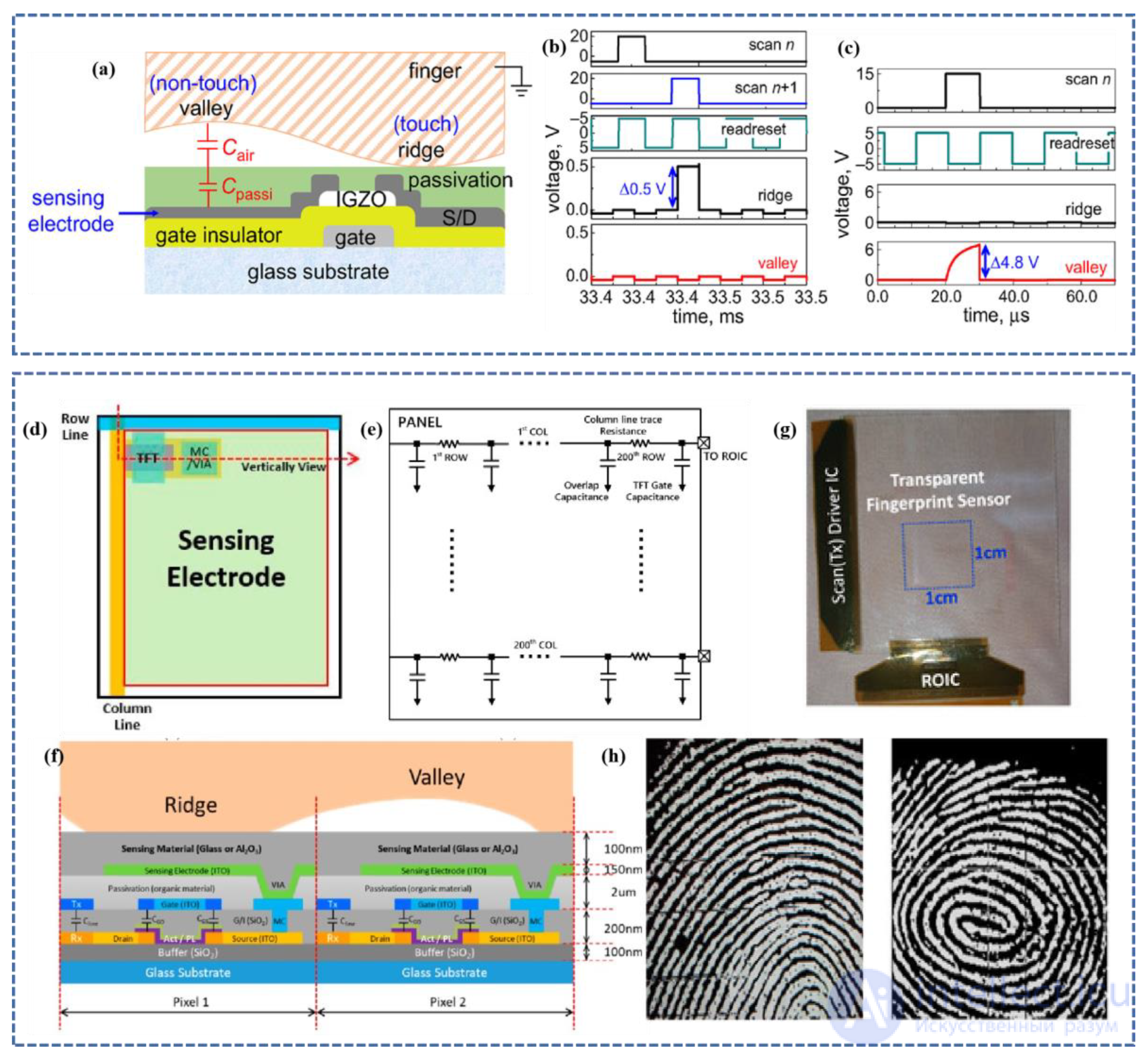
Figure 8 (a) Operating principle of a capacitive sensor for fingerprint recognition. (b) Simulation results for a capacitive sensor for fingerprint recognition circuits. (c) Simulation results for the capacitive sensor of the proposed circuit, (d) top view of a pixel of the proposed sensor, (e) sensor schematic, (f) cross section of a pixel of the proposed sensor, (g) the assembled transparent fingerprint recognition system module and (h) a fingerprint image.
4.2. Mutual-capacitance fingerprint sensor
Devices with a fully bezel-less screen and no physical buttons have become the norm in the smartphone market. On smartphones, unlocking with a fingerprint sensor located on the back or the side of the device is significantly less convenient than unlocking with a sensor on the front. A mutual-capacitance fingerprint sensor uses two electrodes: a transmitting one and a receiving one. The TX pin supplies a digital voltage and measures the charge received at the RX pin; the charge received at the RX electrode is proportional to the mutual capacitance between the two electrodes, and when a finger is placed between the TX and RX electrodes, the mutual capacitance decreases and the charge received at the RX electrode decreases as well. The touch/no-touch state can be determined from the charge on the RX electrode.
Mutual capacitance is easy to apply to fingerprint sensors with two electrodes and an insulator, one electrode being used for driving and the other for sensing. Mutual capacitance makes multi-touch functionality possible [ 189 , 190 , 191 ]. Mutual-capacitance sensors can work on OLED (organic light-emitting diode) and LCD (liquid crystal display) screens with a detection distance that is typically ≤ 300 µm [ 192 , 193 ]. These sensors can be fabricated on glass substrates or by depositing polymer films on window glass [ 194 ]. Transparent capacitive on-screen fingerprint sensors created using mass-production materials and technologies are ideally suited to smartphones and other mobile devices, and they can also be used to build large-area combined touch-and-fingerprint sensors and sensors for flexible/stretchable electronics.
Five varieties (thickness of these layers: 100 µm) of transparent sensing film are available: PET, cellulose nanofiber (CNF) films, and CNF films with embedded BaTiO₃ . BaTiO₃ nanoparticles (CNF + BaTiO₃ , nanoparticle content: 1 wt%, average size: 25 nm) and CNF films with embedded AgNF (CNF + AgNF, silver nanofiber content: 1.2 wt%, average AgNF length: 200 ± 20 µm, average diameter: 380 ± 35 nm) [ 195 , 196 , 197 ]. CNF films have advantages thanks to their high transparency, good mechanical flexibility and strength; however, the low dielectric constant of pristine CNF films (k = 1.4–3.0) limits their use as overlays for fingerprint sensor arrays [ 198 , 199 , 200 , 201 ]. CNF films that include AgNF (CNF+AgNF) have a k value of 9.2 and a transmittance of at least 90%.
For capacitive fingerprint sensors to operate in the high-frequency range in a transparent form, transparent electrodes with high conductivity and optical transmittance (T) are required. The sheet resistance (Rs) of standard transparent electrode materials prevents high-frequency signals from affecting capacitive fingerprint sensors when interference from mobile devices occurs. To achieve high transparency when metals are used as electrodes, the width of the electrode lines has to be limited because of their opacity, according to the data in Table 4 .
Table 4. Mutual-capacitance fingerprint sensor.
| Area/ mm² |
10 × 10 |
10 × 10 |
6 × 6 |
- |
6.4 × 6.4 |
| Channel |
200 × 200 |
64 × 128 |
72 × 72 |
192 × 256 |
80 × 80 |
| Light transmittance (%) |
94 |
94 |
- |
79.90 |
89.05 |
| Electrode material |
Indium tin oxide |
Indium tin oxide |
Metal mesh |
Indium tin oxide |
Hybrid nanostructures |
| Electrode shape |
Diamond |
Diamond |
Half-diamond |
- |
- |
| Capacitance and voltage difference |
50 fF
(ridge and valley) |
210 fF
(contact and non-contact modes) |
- |
4.2 ± 0.07 fF
(ridge and valley) |
- |
| Resolution |
500 DPI |
300–363 DPI |
322 DPI |
- |
318 CPI |
| Features |
- |
Cover glass 0.3–1 mm |
- |
Dual fingerprint acquisition |
Pressure and temperature sensors |
| Ref. |
[ 202 ] |
[ 203 ] |
[ 204 ] |
[ 205 ] |
[ 167 ] |
When a finger touches the contact surface, capacitive fingerprint sensors can also generate a potential difference through the piezoelectric properties of the material, in which the sensor bends under applied stress. Zinc oxide nanostructures that collect the charge produced by the piezoelectric potential generated by each nanoparticle are reported to be able to reconstruct the three-dimensional strain field of a fingerprint [ 206 ]. For the sensor surface to be covered with a chemically inert UV-crosslinkable polymer [ 207 ], the encapsulating layer must be between 1.5 µm and 10 µm thick and must offer excellent hydrophobicity and oleophobicity [ 208 ], as shown in Figure 9 . Hsiung [ 209 ] proposed an 8 × 32 pressure sensor array with a cell size of 65 µm × 65 µm, a sensitivity of 0.39 fF/MPa, a maximum capacitance change of 16% and a resolution of 390 DPI, with no need for additional film processing. Sugiyama [ 210 ] presented a 32 × 32 silicon pressure sensor array with a sensor chip size of 10 mm × 10 mm and an array element pitch of 250 µm, capable of producing stable 2D or 3D images.
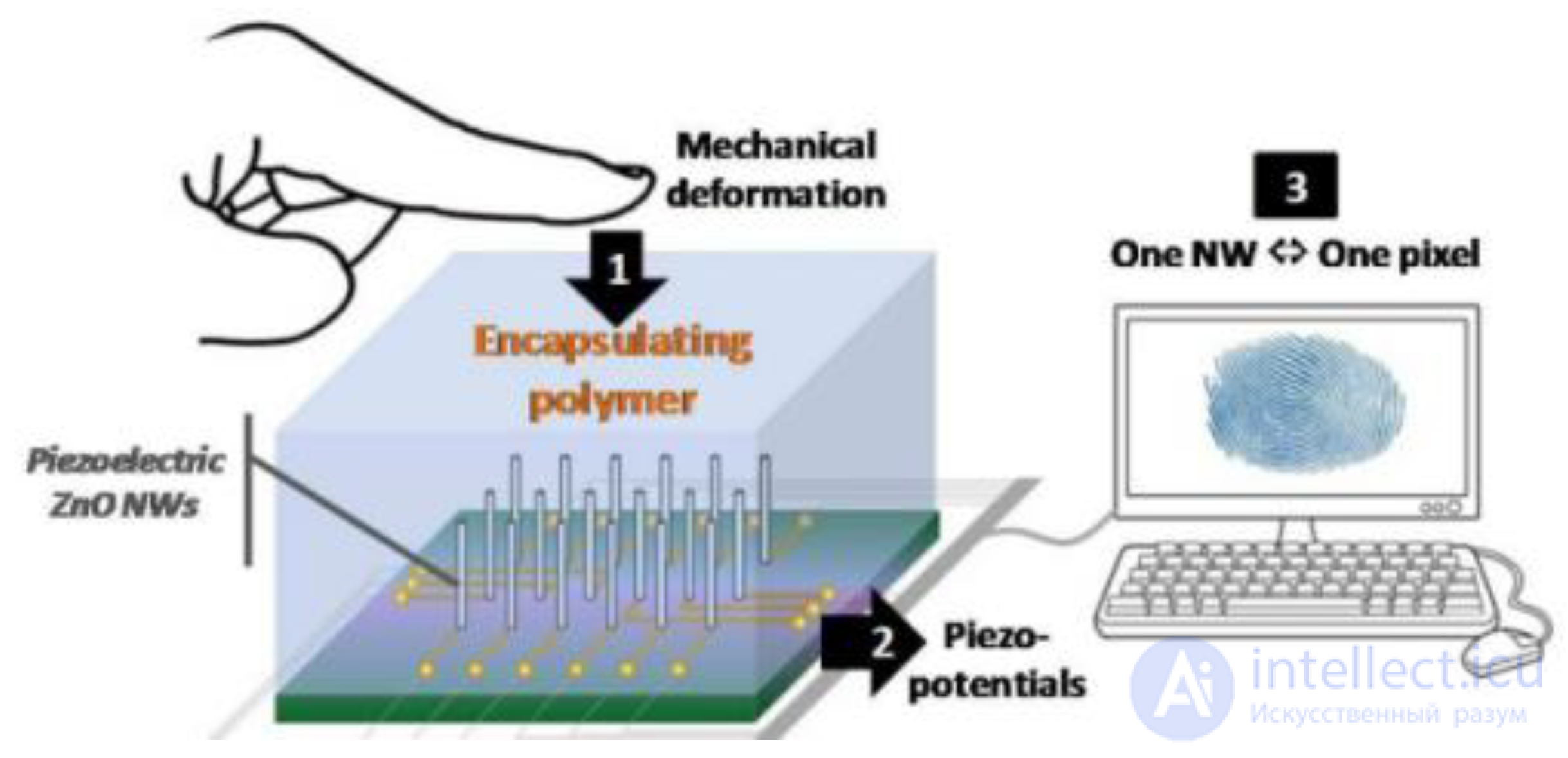
Figure 9. Schematic representation of a pressure-based fingerprint sensor with polymer encapsulation and multiple nanowires [ 208 ].
Where it is used
- smartphones with a home button
- side-mounted scanners
- laptops
- banking devices
- locks
Pros
- compact
- fast
- cheaper than ultrasonic
- harder to fool with a simple photograph
- well suited to mobile devices
Cons
- may work poorly with a wet finger
- sensitive to contamination
- may work less well with very dry skin
- requires contact with the sensor
3. Ultrasonic sensor
A more advanced type. It is often used in modern smartphones, especially under the display.
Operating principle
The sensor sends ultrasonic waves into the finger and analyzes the reflected signal.
the sensor emits ultrasound
↓
the waves reflect off the relief of the skin
↓
the sensor receives the reflection
↓
a 3D map of the fingerprint is built
It can read not only the surface, but also some subsurface features of the skin.
The ultrasonic fingerprint sensor [ 211 ] is the most accurate and precise instrument for capturing fingerprint images. There are two main imaging techniques: pulse-echo imaging and impedance imaging. Ultrasonic fingerprint imaging relies on the reflection of ultrasound as it propagates through media of differing impedance [ 212 ]. When a finger is placed on the sensor area of a mobile phone, a pressure sensor detects the pressure and sends an electrical pulse that activates the ultrasonic fingerprint sensor, which emits an electrical pulse wave. Because of the difference in acoustic impedance between human tissue and air, the echo amplitude in human tissue is greater than in air; the ridge pattern can therefore be determined by measuring the echo amplitude at every point. The intensity of the sensor's ultrasonic waves is comparable to that used in medical diagnostics, which is safe for the human body [ 213 ]. Thanks to the high penetrating power of ultrasonic waves [ 214 ], they can still be detected when there is a small amount of dirt or moisture on the finger, and they can pass through materials such as glass, aluminum, stainless steel, sapphire and plastic, which increases the device's applicability and the likelihood of its successful use. It is also possible to place the sensor inside the gadget to improve its durability.
Ultrasonic imaging is based on detecting the echoes of an ultrasonic pulse, with ridges and valleys producing distinct echoes. It is also possible to explore acoustic impedance approaches by measuring the pulse ring-down, which measures the attenuation of the contact area (that is, the fingertip) [ 215 ]. Fingerprint recognition based on acoustic impedance uses a direct-contact method with air-filled valleys of 430 rayl and ridges of roughly 1.5 Mrayl of human tissue, and the difference in impedance amplitude and phase helps distinguish ridges from valleys, thereby forming the fingerprint image.
The core component of an ultrasonic fingerprint sensor is the ultrasonic transducer, which captures the impulse response of the ultrasonic signal and performs graphical reconstruction using the reflection and diffraction properties of ultrasonic waves. Ultrasonic fingerprint recognition technology is not affected by surface interference and can penetrate the layer of dead skin cells, reflecting the architecture of the fingerprint pattern in the dermis, capturing not only the ridges visible on the surface but also reliable information from inside the tissue.
The earliest ultrasonic fingerprint sensor is a type of ultrasonic probe detection (US5224174A) proposed jointly by Ultrasonic Scan and Niagara, and it is an ultrasonic probe detection system [ 216 ]. The probe emits ultrasonic energy and scans twice in two directions at right angles; after reflection from the finger, the pulse receiver absorbs the reflected signal and converts it into frequency data, and the processing circuit builds the fingerprint image. With the introduction of microelectromechanical systems (MEMS) technology, the MEMS ultrasonic transducer in CMOS made ultrasonic fingerprint recognition applicable to smartphones [ 217 ]. Typical transducers are capacitive micromachined ultrasonic transducers (CMUT) and piezoelectric micromachined ultrasonic transducers (PMUT).
5.1. Fingerprint sensor based on a capacitive ultrasonic transducer
The capacitive micromachined ultrasonic transducer (CMUT) has a simple design, compact dimensions, low noise, high sensitivity, high resolution and excellent matching between the silicon material and the dielectric impedance [ 218 , 219 , 220 ]. Thanks to its simpler structure and mature technology, the CMUT can be produced with conventional semiconductor processes, and it reached the market earlier than the PMUT. Metal top electrodes are a standard component of the basic CMUT structure. A metal top electrode, a vibrating membrane, an edge support, a vacuum cavity, an insulating layer, a bottom electrode and a base make up the standard CMUT design (North Central University dissertation) [ 221 ]. The bottom electrode is attached to the base, whereas the top electrode is able to vibrate together with the membrane. In transmit mode, the alternating electric field between the top and bottom electrodes causes the vibrating membrane to flex and vibrate, thereby generating sound waves; in receive mode, the vibrating membrane oscillates under external sound pressure, causing a change in the electrical capacitance between the top and bottom electrodes, and an electrical signal corresponding to the magnitude of the sound pressure can be obtained through it.
Figure 10a shows a CMUT consisting of several tiny vibrating cells connected in parallel, as well as many microelements connected in parallel in a particular configuration to form a CMUT that delivers greater output sound pressure. It can be made in various shapes, including round, square, hexagonal and so on, depending on the specific requirements.
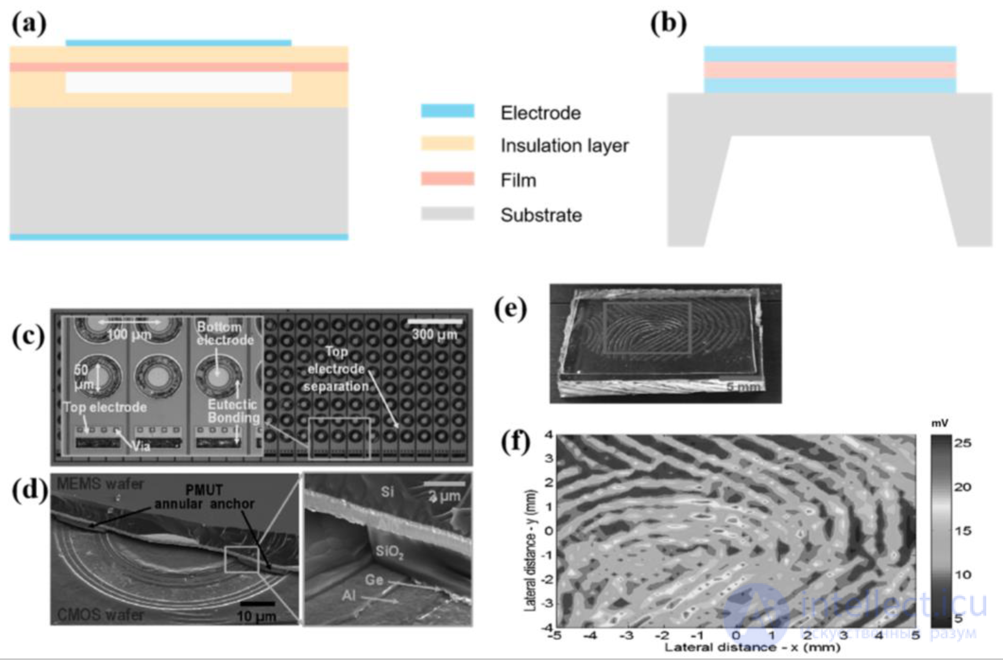
Figure 10. ( a ) CMUT structure; ( b ) PMUT structure. ( c ) Optical images of a 24 × 8 PMUT array after removal of the CMOS wafer, ( d ) cross-sectional SEM images of a single PMUT after partial removal of the MEMS wafer, and ( e , f ) 2D pulse-echo ultrasound image of a PDMS fingerprint phantom .
The first fingerprint sensor based on capacitive micromachined ultrasonic transducers (CMUT) could only capture 2D fingerprint images by mechanical scanning. Savoia [ 223 ] avoided the need for mechanical scanning and proposed a linear probe array for a fingerprint sensor. The transducer consists of 192 rectangular elements with a pitch of 112 µm and a total aperture of 21.5 mm, which corresponds to the average width of a human fingertip. This probe-type fingerprint sensor in an aluminum housing is used in medical therapy. It is also possible to display the grayscale intensity of the captured 3D objects and a 2D display of flat areas. However, the resolution of the resulting photographs needs to be improved. Pulse-echo measurements are impossible because of the array's limited bandwidth. The interface between this huge sensor array and the signal processing circuitry is too complex to meet the size requirements. Kwak [ 224 ] used obstacle-mapping techniques in a waveguide to capture fingerprint images. Fingerprint images can be obtained from hard materials such as glass, which can also be used to capture fingerprints under glass. Adjusting the height and width of the waveguide, as well as the composition of the medium, can improve the resolution of the fingerprint image.
The waveguide method provides higher resolution than the direct-contact method for detecting phase shifts of 0.6 degrees at ridges and valleys at 2.4 MHz. The increased resolution for the fingerprint ridge feature protects and stabilizes the CMUT impedance signal.
5.2. Fabrication of the capacitive ultrasonic transducer
The CMUT fabrication process typically uses a silicon wafer as the base, aluminum as the metal electrode and SiO2 as the edge support, while the vibrating membrane can be made of silicon, SiN and so on. A thin metal layer is deposited on the silicon substrate, forming the bottom electrode plate of the vibrating element. The insulating layer plays a protective role during etching and fabrication and also provides electrical isolation between the top and bottom electrodes, preventing short circuits caused by accidental contact between the top and bottom electrodes during operation. A thin metal layer is deposited on the upper surface of the vibrating membrane, and this is the sensor's top electrode plate. The edge support serves as the support for the vibrating membrane [ 225 ].
The array leads are connected to the flexible part of the printed circuit board, and a preformed probe is molded onto a dedicated acoustic and mechanical substrate of the CMUT chip to fix the rigid part of the printed circuit board to the die. The chip's silicon substrate is removed using an HNA wet etching process. The CMUT is based on direct silicon wafer bonding with local oxidation (LOCOS). It consists of a silicon top plate and a vacuum gap for the silicon nitride and silicon oxide underneath. The vibrating top plate consists of single-crystal silicon with a radius of 24 µm and a thickness of 1.5 µm, positioned beneath a flat plate with a 200 nm vacuum gap. The 64-channel CMUT is bonded to the chip holder with epoxy resin, and the end of the leads is also fixed with epoxy resin to prevent displacement.
5.3. Fingerprint sensor based on a piezoelectric ultrasonic transducer
The CMUT is based on a capacitive electrode separated by a submicron vacuum gap, whereas the PMUT consists of a solid-state piezoelectric capacitor [ 226 ], which simplifies the manufacturing process and improves mechanical stability. As shown in Figure 10b , the PMUT consists of a piezoelectric membrane, top and bottom electrodes and a vibrating membrane. In transmit mode, a certain voltage is applied between the top and bottom electrodes of the piezoelectric membrane, and the pressure created by the converse piezoelectric effect of the membrane causes the membrane structure to flex, deforming the vibrating membrane. When an alternating voltage is applied, the membrane vibrates and radiates sound pressure, thereby converting electrical energy into acoustic energy. In receive mode, the vibrating membrane deforms under external acoustic pressure and deforms the piezoelectric membrane, thereby generating a corresponding charge through the piezoelectric effect and providing conversion of acoustic energy into electrical energy and reception of acoustic signals through the receiving circuit [ 227 ].
As shown in Figure 10c , early AlN-based PMUT arrays for ultrasonic fingerprint sensors were only 24 × 8 in size [ 222 ]. Each PMUT is connected directly to a dedicated CMOS receiver amplifier, which avoids electrical parasitic effects and eliminates the need for through-silicon vias. FC-70 fluoride is used as the coupling layer between the PMUT and the finger, and a 100 µm PVC coating seals the fluoride and protects the sensor [ 228 ]. To keep the surface scratch-resistant and to reduce the effect of scratches and deformations on the sensor surface on the image, a protective layer can be added to the surface of the material [ 229 ]. A 1 µm Al₂O₃ coating is usually chosen, a material with well-known hardness and scratch resistance [ 230 ]. It can be applied to plastic and glass, among other substrates. Sufficiently thin layers of this material have little effect on sound transmission. In 2016, Horsley [ 231 ] proposed a monolithic ultrasonic pulse-echo fingerprint sensor of 110 × 56 cells based on piezoelectric micromachined ultrasonic transducers (PMUT) that were bonded directly to a CMOS readout ASIC [ 232 ]. The array's fill factor is 51.7%, three times that of the 24 × 8 array. The ultrasonic fingerprint sensor captures not only the fingerprint ridges visible on the surface but also information from inside the tissue, presenting three-dimensional information with a substantial increase in security [ 233 ]. Compared with the 110 × 56 array, the 65 × 42 array has a larger pitch to reduce crosstalk. The sensor is capable of multi-channel TX beamforming, which increases the signal-to-noise ratio by 7 dB and allows a slight improvement in the lateral resolution of the image. With a five-column transmit beam, the peak pressure, receiver voltage and image contrast improve by a factor of 1.5. In the unsupported area, the array amplitude is −17 dB compared with −2.7 dB for the 110 × 56. The sensor surface is originally covered with a 215 µm layer of polydimethylsiloxane (PDMS). A fingerprint image of 4.6 mm × 3.2 mm can be produced [ 234 ].
As a rule, the piezoelectric coefficient of lead zirconate titanate (PZT) is two orders of magnitude higher than that of aluminum nitride (AlN). The PZT-based fingerprint sensor (a 50 × 50 PMUT array) uses a single pixel and a mechanical scanning mode, which results in large dimensions, a low frame rate and high cost [ 235 ]. Table 5 compares the various arrays.
Table 5. Structure of the ultrasonic fingerprint sensor.
| Arrays |
24 × 8 |
110 × 56 |
65 × 42 |
50 × 50 |
| Top electrode |
200 nm Mo |
Al |
24 µm Al |
200 nm Pt |
| Piezoelectric layer |
800 nm AlN |
1 µm AlN |
1 µm AlN |
1 µm PZT |
| Bottom electrode |
200 nm Al |
Mo |
Mo |
200 nm Pt |
| Elastic layer |
6 µm Si |
2 µm Si |
1.7 µm Si |
10 µm Si |
| Substrate |
SiO 2 |
SOI |
SiO 2 |
600 nm Al |
| Protective coating |
Al₂O₃ |
PDMS |
PDMS |
- |
| Fill factor |
17% |
51.70% |
- |
- |
| Pixel |
- |
591 × 438 DPI |
376 × 318 DPI |
- |
| Readout time (single element/array) |
-/24 µs |
24 µs/2.64 ms |
24 µs/1.56 ms |
- |
| Image area |
2.3 × 0.7 mm 2 |
4.6 × 3.2 mm 2 |
4.6 × 3.2 mm 2 |
- |
| Resonant frequency |
22 MHz |
14 MHz |
20 MHz |
25.02 MHz |
| Array element pitch |
100 µm |
43 × 58 µm |
100 µm |
50 × 100 µm |
| Pulse excitation |
28 V |
24 V |
24 V |
- |
| Number of cycles |
2 |
3 |
- |
Where it is used
- modern smartphones
- under-display scanners
- devices with enhanced security
Advantages
- can work through the display
- builds a more three-dimensional map
- better protected against simple spoofing
- can work better with a wet finger
Disadvantages
- more expensive
- more complex in design
- can be slower than cheap capacitive sensors
- depends on the quality of the display and of the implementation
4. Thermal sensor
Uses the temperature difference between the ridges and the valleys of the skin.
Principle of operation
the ridges of the finger press against the sensor more firmly
↓
they transfer heat
↓
the valleys barely touch it
↓
a thermal image is produced
Advantages
- can detect a live finger
- harder to fool with an ordinary picture
Disadvantages
- the signal disappears quickly
- depends on the temperature of the skin and of the environment
- less widespread
5. Radio-frequency sensor
Uses radio-frequency signals to analyze the structure of the skin.
Principle of operation
the sensor emits a radio-frequency signal
↓
the signal interacts with the skin
↓
it returns altered
↓
the system builds a map of the fingerprint
Its main distinguishing feature is that it can partly analyze not only the surface but also the deeper layers of the skin.
Advantages
- better protected against surface spoofing
- can work when there is slight contamination
- can take signs of living tissue into account
Disadvantages
- more expensive and more complex
- less common in mass-market devices
Classification by placement
1. Button scanner
the finger is placed on a button
Example: older smartphones, laptops, power buttons.
Advantages:
- fast
- convenient
- cheap
- accurate
Disadvantages:
- takes up space on the body of the device
- makes a completely bezel-less design harder to achieve
2. Side-mounted scanner
the scanner is built into the power button on the
продолжение следует...
Продолжение:
Часть 1 Fingerprint Sensors: Types, Design and Operating Principles
Часть 2 3. Under-display scanner - Fingerprint Sensors: Types, Design and Operating


Comments