
Lecture
Converting signals from analog to digital form involves two operations. The first – sampling in time. It is performed using the sample-and-hold circuits discussed earlier. The second – quantization in level. Analog-to-digital converters (ADCs) are designed for this purpose.
In the simplest case, an ADC consists of a bank of comparators and a logic device that outputs a code depending on which comparators have triggered. Fig. 10.14 shows the circuit of such a 3-bit ADC. ADCs of this kind are called flash (parallel) ADCs.
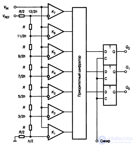
Fig. 10.14. Circuit of a flash (parallel) ADC
The entire range of the input signal is divided into eight levels, which can be encoded with three binary bits. Seven threshold voltages are formed corresponding to these levels and applied to seven comparators. All the comparators compare the input signal with their own threshold. The input signal is assigned the digital code corresponding to the highest-numbered comparator among those that have triggered. If no comparator has triggered, the output code is 000. The logic circuit that forms the output code consists of a priority encoder and three flip-flops, into which the output signal is written by clock pulses.
Thanks to the simultaneous operation of the comparators, a flash ADC is the fastest type. For example, the 8-bit MAX108 converter can perform 1.5 billion conversions per second. The drawback of this circuit is the large size and complexity of its implementation. An N-bit flash ADC must contain 2N-1 comparators and 2N matched precision resistors. For instance, the AD9060 ADC contains 512 comparators.
Therefore, for applications that do not require maximum conversion speed, speed is traded off for hardware savings by clocking the ADC's operation and reusing the same comparators to determine different bits. In the slowest variant, only a single comparator remains, which is used to determine all the bits (Fig. 10.15).
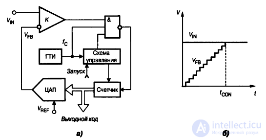
Fig. 10.15. Counting (ramp) ADC: a) block diagram,
b) operating timing diagram
The circuit contains a counter that receives count pulses from a clock pulse generator (CPG). The code formed in the counter is fed to a DAC, whose output signal is used as the threshold for the comparator. The code in the counter starts at zero and increments by one with each clock cycle. As soon as the comparator triggers, the pulses to the counter are stopped and the code reached is presented at the output. On the next processing cycle, the next value of VIN is applied to the comparator input, the counter is reset to zero, and the pulses to the counter resume.
A large number of voltage-to-code conversion methods are currently known. These methods differ significantly from one another in potential accuracy, conversion speed, and hardware implementation complexity. Fig. 10.15 shows a classification of ADCs by conversion method.
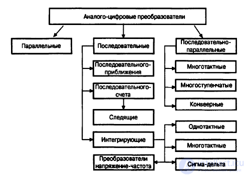
Fig. 10.15. Classification of ADCs
The choice of ADC for a given application is made appropriately, taking into account the required accuracy, speed, power consumption, dimensions, and allowable cost.
The gradual increase in ADC complexity, the appearance of multichannel ADCs, ADCs with a built-in sample-and-hold circuit, and ADCs with a complex digital section, has led to the availability today of complete single-chip data-acquisition systems that convert signals from many sensors into digital code and transmit them to a microcomputer. The block diagram of an advanced data-acquisition system is shown in Fig. 10.16.
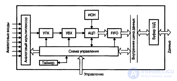
Fig. 10.16. Block diagram of a data-acquisition system
( PGA – programmable-gain amplifier, S/H – sample-and-hold circuit, VREF – voltage reference, DB – data bus)
A sample-and-hold circuit and a voltage reference are built into the circuit. An analog multiplexer is used to connect to several sources of input analog signals. To reduce the interrupt rate on the host processor, some data-acquisition circuits are equipped with FIFO memory (first input – first output). The programmable-gain instrumentation amplifier (PGA) included in the system changes its gain on command from the control circuitry. This makes it possible to equalize the ranges of the analog signals from different inputs.
Examples of such data-acquisition systems include the AD7581, AD1B60 and LM12458 chips.

Контрольные вопросы
1. Схема изолирующего усилителя с трансформаторной связью и описание его работы.
2. Схема компаратора на ОУ.
3. Схема источника опорного напряжения на стабилитроне и компенсационного типа.
4. Схемы механических коммутаторов и коммутаторы с ключами на МОП транзисторах.
5. Функциональная схема аналогового мультиплексора 4х1 и его условное обозначение.
6. Схема оптореле на МОП-транзисторах.
7. Функциональная схема устройства выборки-хранения и временные диаграммы его работы.
8. Простейшая схема ЦАП с суммированием весовых токов.
9. Упрощённая схема генератора прямого цифрового синтеза синусоидального сигнала.
10. Схема параллельного АЦП.
11. Структурная схема АЦП последовательного счёта и временная диаграмма его работы.
12. Классификация АЦП.
13. Структурная схема системы сбора данных.

Comments