
Lecture
A digital-to-analog converter (DAC) is designed to convert a number, usually represented as a binary code, into a voltage or current proportional to that number. Fig. 10.11 shows a general classification of DACs by input-code conversion method and output-signal generation circuit.
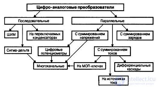
Fig. 10.11. Generalized classification of DACs
DACs can be further classified according to a number of specific criteria, for example:
by type of output signal: converters with a current output or with a voltage output,
by type of digital interface: with serial input or with parallel input,
by number of DACs per chip: single-channel and multichannel,
by speed: low, medium and high speed,
by resolution (bit width).
The simplest design is that of parallel DACs that sum weighted currents using resistive networks (Fig. 10.12).
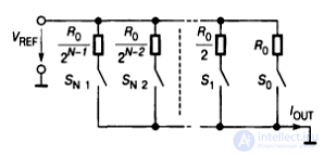
Fig. 10.12. The simplest DAC circuit with summation of weighted currents
In this circuit the resistor values are chosen so that, when the switches are closed, the current flowing through them corresponds to the weight of the bit. A switch must be closed when the corresponding bit of the input code equals one. The output current is given by the relation
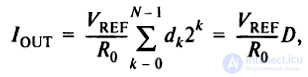
where k – the bit width of the input code, dk takes the value 0 or 1 depending on the state of the k-th bit of the input current, D – the input code
( more precisely, the total weight of the input code). At high DAC resolution, the current-setting resistors must be matched with high precision. The most stringent accuracy requirements apply to the resistors of the most significant bits, since the spread of weighted currents must not exceed a fraction of the current of the least significant bit.
Despite its simplicity, the DAC circuit with summation of weighted currents considered above has a number of drawbacks:
for different input codes, the current drawn from the voltage reference (VREF) will differ, and this can affect the magnitude of the VREF output voltage,
the values of the weighting resistors can differ by a factor of a thousand, which makes it very difficult to implement these resistors in semiconductor ICs; moreover, the resistance of the most-significant-bit resistors can be comparable to the resistance of the closed switches, which leads to additional conversion errors,
in this circuit, a significant voltage is applied across the open switches, which complicates their design.
Nowadays a large number of DACs based on various principles are produced by different manufacturers, which in one way or another circumvent these drawbacks and provide high accuracy and speed characteristics.
A DAC appears in a circuit whenever a processed digital signal needs to be converted into analog form and fed to an actuator, which may be a loudspeaker, an electric motor, etc. Another use of DACs is the direct synthesis of signals of a required shape, which is first generated digitally and then converted to analog form by the DAC. As an example, Fig. 10.13 shows a simplified circuit of a direct digital synthesis (DDS) generator producing a sine-wave signal over a wide range of settable frequencies.
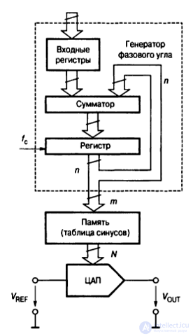
Fig. 10.13. Simplified circuit of a DDS sine-wave signal generator
A direct digital synthesis circuit contains three main blocks: a phase angle generator, a memory, and a DAC. The phase angle generator is typically an accumulating adder with a register. It functions simply as a phase register whose contents are incremented by a certain phase angle at set time intervals. The required phase increment Δφ is loaded as a digital code into the input registers, either serially or byte by byte. The memory acts as a lookup (function) table.
Direct digital synthesis systems are extremely flexible. The frequency of the output signal can be changed almost instantaneously, without a phase discontinuity, simply by changing the contents of the input registers.

Comments