
Lecture
Source, or generator, of reference voltage (voltage reference) — a basic electronic unit that maintains a highly stable, constant electrical voltage at its output. Voltage references are used to set the output voltage of stabilized power supplies, the scales of digital-to-analog and analog-to-digital converters, the operating modes of analog and digital integrated circuits and systems, and as voltage standards in measuring instruments. The accuracy of measurement and conversion, and the stability of these devices, are determined by the precision parameters of the voltage references used in them.
The most accurate voltage sources are cryogenic laboratory standards based on the Josephson effect. From 1976 until the end of the 1990s, the market for mass-produced precision voltage references was dominated by devices based on buried-structure Zener diodes, the best examples of which approached the Weston normal cell in overall precision parameters. In the 2000s, bipolar-transistor superbandgap voltage references, XFET voltage references based on differential pairs of field-effect transistors, and FGA voltage references based on floating-gate transistors reached a comparable level of accuracy and stability. In devices with relatively modest requirements for reference-voltage accuracy and stability, inexpensive integrated bandgap references and ordinary Zener diodes, in discrete or integrated form, are used.
The main purpose of voltage references is to create a standard voltage that can be used by electronic information-conversion devices as a reference. Such devices include comparators, regulators, and analog-to-digital and digital-to-analog converters, among others.
The simplest method of obtaining a reference voltage consists in applying an unstabilized input voltage, through a current-limiting resistor, to a Zener diode, which acts as a so-called parametric stabilizer, whose main parameter is the breakdown voltage of the p-n junction (Fig. 10.3).
The current-voltage characteristic of the Zener diode is shown in Fig. 10.4.
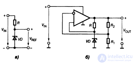
Fig. 10.3. Zener-diode voltage reference circuit: a) parametric voltage reference,
b) compensated-type voltage reference
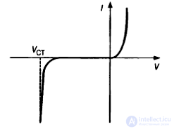
Fig. 10.4. Current-voltage characteristic of the Zener diode
At a certain reverse voltage, called the stabilization voltage VST, breakdown of the p-n junction occurs; however, owing to structural and technological features, this breakdown does not cause the device to fail. The section of the current-voltage characteristic corresponding to the breakdown mode is nearly vertical, so that as the current through the Zener diode changes, the voltage across it changes only slightly.
The quality of stabilization is evaluated by the stabilization coefficient
KST = ΔVIN/ΔVREF
The stabilization coefficient for a parametric voltage reference (Fig. 10.3a) can be 10…100. In a compensated-type voltage reference it can reach a value on the order of 10000.
In the era of vacuum tubes, radio-equipment designers had access to two types of reference-voltage sources: gas-discharge stabilizer tubes and chemical voltage sources (storage batteries and single-use galvanic cells). The best initial voltage accuracy was provided by mercury-zinc Clark cells at 1.434 V and mercury-cadmium Weston normal cells at 1.019 V. Massive yet fragile, intolerant of shocks and vibration, and filled with toxic substances, Weston cells were used exclusively under laboratory conditions, while mass-produced radio equipment used less accurate but cheap and relatively safe sealed galvanic cells and batteries. Mercury-zinc cells at 1.35 V, which found application during the Second World War, could deliver a current of several mA for more than a thousand hours, but were inferior in accuracy and stability to laboratory voltage standards. To set voltages from 80 V to 1 kV, inert-gas-filled glow-discharge stabilizer tubes were used; for voltages from 400 V to 30 kV, hydrogen-filled corona-discharge stabilizer tubes were used. Devices based on gas-discharge stabilizer tubes required no regular maintenance, but their deviation from the nominal voltage could reach ±5 %.
In 1953, Clarence Zener invented the semiconductor Zener diode, or the “Zener diode” — a semiconductor diode operating in a mode of reversible reverse breakdown and maintaining a constant voltage across its leads over a wide range of currents and temperatures. The precision and noise characteristics of “ordinary” Zener diodes, without structural and technological improvements, were and remain mediocre. Research in the 1960s showed that the best characteristics belong to Zener diodes whose reverse breakdown voltage is approximately 6 V. An even more precise pair was found in a 5.6 V Zener diode connected in series with, and in the forward direction of, a silicon diode or several diodes. The temperature coefficient of voltage (TCV) of such devices dropped below the level of 10 ppm/°C, which fully satisfied the designers of the time. However, the stabilization voltage of temperature-compensated Zener diodes cannot be reduced below ~7 V, nor the current below several mA, which complicated their use in low-voltage and micropower devices, while the high price, caused by lengthy factory electrothermal aging, hindered their use in mass-produced equipment.
In 1962, the twenty-two-year-old Cambridge student Brian Josephson predicted the possibility of creating a precision voltage standard based on superconducting junctions. In 1968, practical research into Josephson junctions began; in 1971—1972 the national metrology services of Australia, the United Kingdom, Canada, the United States and the FRG carried out cross-comparisons of these devices; in July 1972 the U.S. metrology service made the Josephson-junction standard a national standard, and in January 1990 it became the world standard. The Josephson standard, with a stated relative uncertainty of 5•10−9, is the most stable and accurate voltage source, but it requires liquid-helium cooling and is therefore applicable only under laboratory conditions.
In 1966, National Semiconductor brought to market the LM100, designed by Bob Widlar — the first integrated voltage regulator. The reference voltage of the LM100 was set by a planar Zener diode formed directly in the chip die. In early 1970, Widlar put into production the first three-terminal integrated regulator, the LM109. This chip was the first to use the three-transistor bandgap invented by Widlar — a voltage source approximately equal to the width of the bandgap[10]. A year later, National Semiconductor released the LM113, designed by Widlar and Bob Dobkin — a two-terminal bandgap chip with a voltage of 1.220 V and a TCV not exceeding 100 ppm/°C[10]. In 1974, Paul Brokaw invented another, two-transistor bandgap topology, which provided substantially better voltage-reference accuracy and therefore won the market. Widlar continued his development work, and in 1976—1977 proposed a family of new topologies, on the basis of which the first sub-bandgap reference was built — a precision voltage reference at a voltage substantially lower than the bandgap width (200 mV — the LM10, 1977).
In the early 1970s, industry did not yet need highly stable, precision voltage references. Demand for them arose in the middle of the decade, with the start of production of the first integrated digital-to-analog and analog-to-digital converters[11]. Neither Zener diodes nor first-generation bandgap references satisfied the temperature-drift requirements of DAC and ADC designers. A substantially more accurate device, the buried-structure Zener diode (buried Zener), was first released in discrete form in 1974, and in 1976 National Semiconductor released the LM199, designed by Dobkin — the first integrated buried Zener at 6.95 V[12] (the Soviet counterpart being the 2S483[13]). Thanks to a built-in thermostat and current amplifier, the new chip had a guaranteed maximum TCV of 1 ppm/°C and a typical TCV of 0.3 ppm/°C, with a noise level in the audio frequency range of no more than 7 µV rms[14]. With the release of the LM199, voltage-reference circuit design split into two branches: expensive integrated buried-Zener voltage references for the most critical tasks (measurement ADCs, voltage standards), and cheap but less accurate bandgap references for everything else (voltage regulators, power-supply monitors). The LTZ1000, designed by Dobkin and brought to market in 1987, remains to this day the most accurate mass-produced integrated voltage reference and is used in the most accurate solid-state laboratory standards. Its manufacturer, Fluke, states a long-term instability of 1 ppm/year and a TCV of 0.1 ppm/°C[15] [16]. Here it must be taken into account that the absolute value of the LTZ1000’s output voltage itself is defined only approximately, and only a measurement on more accurate (primary) equipment, with the measured value recorded in the certificate for the specific unit, turns it into a reference standard possessing the required metrological characteristics. See, for example, Table 8 in the article[17]. In this respect this voltage reference differs from the less accurate, but nevertheless primary in the conditions of their application, LTC6655-series voltage references and others, for which the technical documentation states the resulting voltage and its uncertainty.
During the 1980s and 1990s, improvements in circuit design and technology, together with the introduction of laser trimming, narrowed the qualitative gap between the two types of devices[18]. In the early 2000s, “superbandgaps” — a new generation of bandgap references with superior initial accuracy and low noise — came to market[19]. By 2005, “superbandgaps” had matched buried-Zener references on individual accuracy parameters, but could not surpass them on the combination of parameters[19].
In 1997, Analog Devices brought to market a fundamentally new type of voltage reference under the trademark XFET[20]. The circuits of these devices resemble the Brokaw bandgap, in which bipolar transistors are replaced by field-effect transistors. However, despite the similar topology, XFET uses a completely different operating principle — an indirect measurement of the dielectric permittivity of the silicon in the field-effect transistor channel. This parameter, like the voltage across a p-n junction, decreases with rising temperature, but is more predictable, and its TCV is more stable than the TCV of a p-n junction in a real circuit. Analog Devices began developing the new devices in order to get around the fundamental limitations inherent to both bandgap references and buried-structure Zener diodes, and the project succeeded overall. The TCV of second- and third-generation XFET (3 ppm/°C) is still substantially worse than the TCV of the best Zener-diode voltage references, but it has a better, nearly linear, shape of the voltage-versus-temperature dependence, with lower noise, lower long-term drift, and at the same time XFET is much cheaper[21].
In 2003, the company Xicor (a division of Intersil since 2004) released another fundamentally new type of voltage reference, named FGA[22]. The operating principle of these devices, like that of non-volatile memory chips, is based on the long-term storage of charge on the isolated gate of a field-effect transistor. The FGA literally “remembers” an analog voltage “written” deep within the CMOS structure[22]. The guaranteed “memory” retention time of the first-generation FGA was ten years, and its precision parameters were comparable to the best bandgap references, with a lower supply current (less than 0.8 µA per memory cell with a buffer amplifier)[22].
Thus, at the start of the 21st century, four different types of precision integrated voltage references competed on the market: the buried-structure Zener diode, the superbandgap, XFET, and FGA. By 2005, the psychologically important threshold — a TCV of 1 ppm/°C — had been surpassed by several buried-Zener ICs, several superbandgaps, and the five-volt version of the first-generation FGA[22] (no longer manufactured as of 2012[23]). In the United States alone, precision voltage references of proprietary design are mass-produced by Advanced Linear Devices, Analog Devices, Fairchild Semiconductor, Intersil, Linear Technology, Maxim Integrated Products, Microchip Technology, Microsemi, National Semiconductor, ON Semiconductor, Philips, Semtech, Texas Instruments (which absorbed Burr-Brown) and Apex Microtechnology (a manufacturer of chips designed by the now-defunct Thaler Corporation)[24].
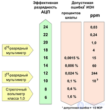
Dependence of the permissible error of a measurement ADC on the required effective (not nominal!) resolution
The primary function of a voltage reference — generating a voltage that is known in advance — determines its main characteristics: “accuracy” and “stability”[25]. These concepts, as well as the concepts of “error,” “drift,” and “noise,” are defined differently across different industries: metrologists, designers of measuring instruments, and designers of ordinary, non-precision electronic devices place similar, but not identical, requirements on voltage references[26]. No state standards defining the parameters specifically of voltage references exist in the Russian Federation. For two-terminal integrated voltage references (analogs of Zener diodes), the norms developed for discrete Zener diodes may be applied; for three-terminal voltage references, the norms for linear voltage regulators. The sets of voltage-regulator parameters in GOST 19480-89 “Integrated circuits. Terms, definitions and letter designations of electrical parameters” and in GOST R 52907-2008 “Power supplies. Terms and definitions” differ, in particular, in the definitions of the overlapping, but not identical, parameters of output voltage drift[27] (GOST 19480-89) and long-term-operation instability (GOST R 52907-2008)[28].
Technical documentation for integrated voltage references, most of which are designed by U.S. companies, is drawn up according to the norms established specifically in American industry. The most complete set of voltage-reference characteristics reflects the requirements of precision-ADC designers, and the most important parameters for them, in decreasing order of significance, are: the initial spread of the reference voltage (the initial deviation of the reference voltage from its nominal value), the temperature coefficient of the reference voltage, and its long-term drift (“instability during long-term operation” in the terminology of GOST R 52907-2008[28])[29]. The less strict the accuracy requirements placed on a voltage reference, the narrower the set of rated parameters. For inexpensive voltage regulators, a single accuracy parameter may be rated — the initial spread[30] — or the permissible range of output-voltage variation (upper and lower bound). It is precisely this latter variant (a range of values) that was adopted as the basis by the compilers of GOST 19480-89[31].
The initial spread of the output voltage is defined as the maximum deviation of the DC voltage at the output of a voltage reference from its nominal value at the first power-up of the IC. The initial spread is usually measured at normal temperature (+25 °C) and at the nominal input voltage and output current specified by the manufacturer. For Zener diodes the initial spread can reach 5% of the nominal value; for integrated voltage references it lies in a range from ±1% (worst-case accuracy) to ±0.01%, or ±100 ppm[30]. Unless otherwise stated in the documentation, the initial spread does not include the permissible voltage shift that occurs when the chip is soldered to the board.
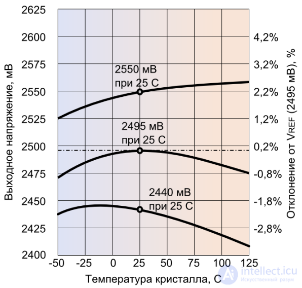
Temperature curves of a simple TL431 bandgap reference. In the center — an ideal sample with a parabolic characteristic; above and below — the permissible deviations. Technological spread of interrelated parameters not only shifts the curve up or down, but also shifts its hump left or right
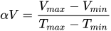
TCV in the narrow sense is a differential parameter equal to the ratio of the relative change in output voltage to the small change in ambient temperature that caused it, all other conditions being equal[30]. In the documentation for integrated voltage references, this parameter is usually defined differently, by the “box method”: TCV equals the ratio of the difference between the maximum and minimum output voltage, guaranteed by the manufacturer over the entire operating temperature range at the nominal input voltage and output current, to the width of the operating temperature range:[32]
 [32]
[32]
A parameter defined this way as an integral quantity is suitable only for estimating the maximum voltage shift at the edges of the operating temperature range, and it is not recommended for use over narrower temperature intervals[33]. The reason is that a nearly linear form of dependence is characteristic only of precision devices of the XFET and FGA types, as well as of simple bandgap references that deviate substantially from the calculated “centering” and have not undergone fine trimming. With correct “centering,” or with individual trimming of it, simple bandgap references and Zener-diode voltage references exhibit a parabolic characteristic, while bandgap references and Zener-diode voltage references with nonlinearity-correction circuits exhibit an S-shaped characteristic (a parabola with its hump clipped)[33]. The differential TCV of such a curved characteristic can differ substantially from the integral parameter[33].
The TCV of cheap mass-produced integrated voltage references of all types is limited to a value of 10 ppm/°C[34]. Reducing the TCV of bandgap and Zener-diode voltage references to a level below 5 ppm/°C requires a substantial increase in technology cost, and the practical limit of guaranteed TCV for mass-produced items is 1 ppm/°C[34]. Lower TCV values are possible only in certain series of ultra-precision voltage references based on buried-layer Zener diodes (Thaler VRE3050J — 0.6 ppm/°C over the range −40…+85 °C[35]).
A further reduction in TCV is possible only through thermal stabilization of the voltage reference, which narrows the range of die-temperature variation to a few degrees or fractions of a degree. The first integrated voltage reference with a built-in spiral die heater and thermoregulator, the LM199, already achieved a TCV of 1 ppm/°C in 1976, with a typical value of 0.3 ppm/°C[14]. The LTZ1000, a mass-produced buried-layer Zener with a built-in heater, manufactured since 1987, has a maximum guaranteed TCV of 0.05 ppm/°C[36]. In the LM199 the die temperature is stabilized at +86 °C[37]; however, according to Fluke, such high temperatures are not optimal: lowering the operating temperature to +50 °C halves the long-term drift of the Zener diode. Fluke states that its laboratory standards based on the LTZ1000 have a guaranteed instability of no more than 1 ppm per year[16].
Besides the voltage reference's own instability, parasitic thermocouples also contribute to the reference-voltage error; these are formed by the junction of dissimilar metals in the device's electrical leads and the mounting conductors. When there is a temperature difference between different leads, the EMFs of the parasitic thermocouples add to, or subtract from, the reference's own voltage. Thus, thermocouples may form at the points where the chip's leads are soldered to the printed circuit board, introducing an additional error whose magnitude depends on the temperature difference between the solder joints. The instability produced by these uncompensated thermocouples is most significant for voltage references in metal packages with Kovar leads. It is usually not stated in the datasheet specifications for a voltage reference's TCV[38].
.
Russian GOSTs do not establish a precise boundary between drift (“the largest change in the output voltage of an integrated circuit over a given time interval in the absence of other destabilizing factors”'[27]) and noise (“the voltage at the output of an integrated circuit in a given frequency band, with the input voltage equal to zero”[39]) of an integrated voltage reference. In IC documentation, the boundary between drift and noise is drawn at a frequency of 0.1 Hz[40].
Long-term drift
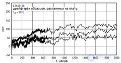
Drift of three samples of the LT1461 superbandgap reference, recorded at constant ambient temperature over 2000 hours. The measurement frequency in the first 650 hours is higher than in the subsequent 1350 hours
During long-term operation, a voltage reference exhibits two different kinds of drift: short-term drift — random deviations of the output voltage with a frequency spectrum lying below 0.1 Hz — and long-term drift, which usually takes the form of a systematic rise or fall of the reference voltage over time intervals of hundreds or thousands of hours[41]. The relative rate of long-term drift, defined in GOST R 52907-2008 as “partial instability during long-term operation”[28], is the third most important component of a voltage reference's instability[41].
Over time, the rate of long-term drift decreases and the output voltage stabilizes. Manufacturers usually rate the maximum drift permissible during the first 1000 hours of operation, expressed in ppm per thousand hours (ppm/1000hr, ppm/kHr). The lowest drift figures, from 5 to 10 ppm per 1000 hours, are characteristic of voltage references based on buried-structure Zener diodes and voltage references based on floating-gate transistors. The rate and direction of drift after this period are usually not rated. Linear Technology's documentation states that the drift rate decreases exponentially, with the drift over the second thousand hours being roughly a third of that over the first thousand, and so on[42]. Intersil's documentation rates the absolute magnitude of drift over the chip's entire service life, with the drift over the first thousand hours given for reference[43].
Measuring drift is a nontrivial task, requiring especially stable measuring instruments and prolonged thermal stabilization of the measurement setup. Bob Pease recalled that in the first year of LM199 production, “…we used an excellent [for its time] six-digit digital multimeter… and it turned out that all the chips under test drifted in sync. Reference voltage sources of other types [galvanic cells, bandgap references, Zener diodes] also drifted in sync [with the LM199 samples]. The culprit was the voltage reference inside the digital multimeter.”[44]
There is no consensus on whether drift can be stabilized through accelerated electrothermal aging. Linden Harrison states that experienced designers burn in chips at 125 °C for one week before soldering them to the board, on the assumption that “annealing” relieves the mechanical stresses accumulated in the die[41]. Bob Pease recommended performing “burn-in and thermal cycling,” not only to reach the drift plateau but also to weed out unstable samples[45]. Linear Technology engineer John Wright argues that the Arrhenius equation is not applicable to burning in chips, and that accelerated “drift stabilization” is not possible. In Wright's view, burn-in is meaningful only at the level of the finished printed circuit board[46].
Noise
The noise of precision voltage references is usually rated in two frequency bands: 0.1—10 Hz and 10—1000 Hz[40]. Noise filtering with active or passive RC filters is applicable only in the upper band. At frequencies below 10 Hz, the required filter-capacitor values, and with them the expected leakage currents through these capacitors, grow so large that the “contribution” of leakage currents to the voltage reference's instability outweighs any benefit from filtering.
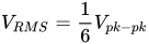
Noise voltage is usually specified as the full peak-to-peak noise voltage swing[40]. The RMS noise voltage is roughly 6 times smaller than this value:
 [40]
[40]
The peak-to-peak noise voltage swing of “ultra-precision” voltage references, measured in the 0.1—10 Hz band, is 1.5 to 5 µV[47] (for reference, the same figure for an integrated linear regulator is typically 0.01% of the output voltage, or 500 µV at a 5 V output voltage[48]). In good measurement ADCs, the peak-to-peak noise swing should not exceed 10% of the least-significant-bit value[49][50], so a low-noise voltage reference at 5 V with a noise level of 1.5 µV (0.3 ppm peak-to-peak, for example the LTC6655[42]) meets the requirements of no more than an 18-bit converter[51].
The silicon die, the die holder, the chip package, and the printed-circuit-board material have differing coefficients of thermal expansion. Uneven expansion during heating produces mechanical stresses in the die, which persist even after cooling back to normal temperature[46][33]. As a result, thermal hysteresis occurs: the voltage reference's voltage at the end of a heat-cool cycle does not match the voltage at the start of the cycle[52].
Rating this phenomenon is a relatively recent practice[52]. In chip datasheets, thermal hysteresis is defined as the maximum expected difference between the output voltages at the beginning and end of a test thermal cycle. Typical values are around ±25 ppm, or ±0.0025% of the output voltage[52]. The initial and final voltages are always measured at normal temperature (+25 °C), while the duration and temperature swing of the test cycle can differ substantially. In rare cases, manufacturers rate hysteresis for cycles of varying intensity (the LT1461 — for cycles of 0…70 °C, −40…85 °C and −40…125 °C) and publish histograms of its distribution by amplitude and sign[46][53].
Special cases of thermal hysteresis are observed when mounting the die onto the die holder and when soldering the chip onto the printed circuit board. Chips in metal packages with flexible leads are little affected by these effects, whereas in chips with rigid leads the reference-voltage shift caused by packaging can reach 0.5%[54]. The voltage shift caused by soldering is usually not specified: hysteresis is measured on chips mounted in the sockets of a test fixture. Analog Devices' documentation states that the specified initial voltage tolerance does not include the shift caused by soldering[55]. Linear Technology's documentation gives histograms of the amplitude distribution of this shift (LT1461 — spread from −300 to +100 ppm, −110 ppm on average) and estimates the rate of its “shrinkage” under normal operation[53].
The main parameters specified for modern precision voltage references, their typical values for various topologies, and the characteristics of selected representatives of each topology are given in the comparative table[56]. To make both the absolute and the relative parameters of the different chips comparable, only chips with a +5 V output voltage were selected. All the listed Zener-diode and bipolar-transistor devices are characterized by large (several mA) supply currents. Reducing the current is possible, but it inevitably comes with increased noise. A combination of small (tens of µA) currents and low (down to 10 µV) noise levels is possible only in floating-gate-transistor voltage references, and even within this topology there is an inverse relationship between noise level and current. By default, all accuracy parameters can take both negative and positive values, and the ± sign is omitted in the technical documentation.
| Parameter | Unit of measure |
Main topologies of precision integrated voltage references | |||||||
|---|---|---|---|---|---|---|---|---|---|
| Buried-structure Zener diodes | Superbandgaps | Differential JFET pair (XFET) | Floating-gate transistor (FGA) | ||||||
| Typical values[a 1] |
Thaler VRE3050[a 2] |
Typical values[a 1] |
Linear LTC6655[a 3] |
Typical values[a 1] |
Analog Devices ADR425B[a 4] |
Typical values[a 1] |
Intersil ISL21009[a 5] |
||
| Initial tolerance | % | 0.02% | 0.01% | 0.04% | 0.025% | 0.04% | 0.04% | 0.01% | 0.01% |
| Temperature coefficient without die temperature stabilization |
ppm/°C | <2 | 0.6 max. 0.3 typ. |
<3 | 2 max. 1 typ. |
<3 | 3 max. 1 typ. |
3 | 3 |
| Shape of the temperature curve | S-shaped | Close to linear | |||||||
| Long-term drift | ppm/1000 h | 20 | 6 | 40 | 60 | 40 | 50 | 10 | about 10[a 6] |
| Thermal hysteresis | ppm/cycle | - | 1[a 7] | - | 30[a 8] 60[a 9] |
- | 40 | - | 50[a 10] |
| Noise voltage in the 0.1−10 Hz band | µV peak—peak | 3 | 3 | 10 | 0.1 | - | 3.4 | - | 4.5 |
| Noise voltage in the 10−1000 Hz band | µV rms | 3 | 5 | 10 | 0.67 | - | Not specified | - | 2.2 |
| No-load current (minimum supply current)[a 11] | mA | 2.4 max. | 4 | 0.75 | 7 | - | 0.6 | - | 0.18 max. 0.095 typ. |
| Fine on-board trim capability | yes | ±5 mV | possible | no | yes | ±0.5% VREF | yes | ±2.5% VREF | |
| Operating temperature range | °C | 0…+70 | -40…+85 | -40…+85 | −40…+125 | −40…+125 | −40…+85[a 12] | −40…+125 | |
Table notes
|
|||||||||
Zener diode
Glow-discharge Zener diode
Bandgap
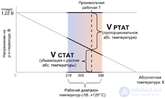
Principle of summing voltages with opposite temperature coefficients
The operating principle of bandgap references — voltage sources whose output is defined by a semiconductor's bandgap width — is based on the fundamental dependence of the voltage across a forward-biased p-n junction on current and temperature. At a fixed current, this voltage decreases linearly as temperature rises, with a TCV of roughly −2 mV/°C. If this voltage is added to the voltage on another circuit element whose voltage is proportional to absolute temperature, then, with correct scaling of the two terms, their temperature coefficients cancel each other out, and the sum of the two voltages, to a first approximation, equals the bandgap width of the semiconductor used at T=0 K and is independent of temperature.
The “other element” is usually a pair of diode-connected bipolar transistors operating at different current densities. The difference between the emitter-junction voltages of these transistors depends only on temperature and on the ratio of current densities. Its absolute value in real circuits does not exceed 100 mV, so to precisely compensate the two temperature coefficients it must be amplified 5…15 times. In the most common bandgap circuit, proposed by Paul Brokaw in the mid-1970s, this same pair of transistors serves as the source of both the voltage proportional to absolute temperature (PTAT voltage) and the voltage that decreases with rising temperature (CTAT voltage), while scaling and summing the terms is performed by a simple two-resistor divider. The inevitable spread of process parameters accounts for the mediocre accuracy of such circuits: the initial tolerance is typically ±3% of the output voltage, and in the best circuits ±1.6%[57]. In so-called sub-bandgap references, which generate a reference voltage of a few hundred mV, the spread is even higher — up to ±3.6%[58]. With precise “centering” of the components, the temperature curve of the reference voltage has a characteristic parabolic shape with a maximum at the center of the operating temperature range. At the edges of the operating range the voltage drops by about 0.2% from the maximum. With deviations from ideal centering, the hump of the temperature curve can shift outside the operating temperature range, and the observed temperature curve approaches linear. The temperature coefficient of the voltage can be reduced with nonlinearity-compensation networks, the voltage spread can be reduced by individual chip trimming, but the high noise level inherent to bandgaps can practically not be reduced.
Despite all their shortcomings, simple bandgap references are used en masse in linear-regulator and voltage-monitor chips (the 78XX and TL431 families) and in operational amplifiers. In low-voltage circuits bandgap references are indispensable: unlike Zener diodes, “ordinary” bandgap references work at supply voltages down to +2 V, and sub-bandgap references at supply voltages down to +1.0 V.
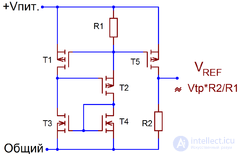
Voltage reference on complementary MOS transistors in a memory chip
A modern memory chip contains a whole set of built-in reference-voltage sources and regulators. Most memory chips operate at a reduced supply voltage, set by a built-in voltage reference and stabilized by a high-power regulator. Lowering the supply voltages is needed, first of all, to avoid breakdown of transistors made with sub-micron process technology. The second area where voltage references are used is setting the threshold voltage for the differential sense amplifiers used in memory ICs with a capacity above 1 Mbit[59].
In simple voltage references built in CMOS technology without bipolar temperature-sensitive elements, the output voltage is set proportional to the threshold voltage of the p-channel transistor VTP[60]. In memory chips this parameter is about −0.4 V, not counting the body effect. The actual value, taking the source-body voltage into account, VTP can be twice as large[61]. Transistor T1 operates at a low channel current, so its gate-source voltage is approximately equal to the threshold voltage, and this same voltage is dropped across resistor R1 and the gate of T5. T5 mirrors the current flowing through T1, so the output voltage taken from R2 equals
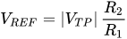 [59]
[59]
The first devices of this kind, developed in the early 1990s, had a supply-voltage sensitivity of about 1% (10 mV/V) and a TCV of 0.15 mV/°C[59].
Buried-structure Zener diode
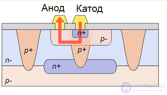
Cross-section of a buried-structure Zener diode. The arrow shows the path of the breakdown current. The ratios of the vertical and horizontal scales and of the layer thicknesses are conventional.
The breakdown current of an ordinary planar Zener diode is concentrated in the near-surface layer of silicon — the layer with the highest concentration of crystal-lattice defects and foreign impurities. It is precisely these impurities and defects that cause the Zener diode's instability and noise. Its parameters can be improved by “driving” the breakdown current deeper into the crystal, into a buried p-n junction structure with a lower breakdown voltage than in the near-surface layer[62]. In the classic epitaxial process used to make the LM199, a deep p+-type island is formed at the site of the future Zener diode, and then the usual base (p-) and emitter (n+) diffusions are carried out[62]. The emitter of the resulting diode structure becomes the Zener diode's cathode, and the base becomes the anode. In the near-surface layer this junction has an n+-p- conductivity profile, while at the bottom of the base region it has an n+-p+ profile[63]. The heavily doped n+-p+ junction has a lower breakdown voltage than the near-surface n+-p- layer, so the entire reverse current of the Zener diode flows right at the bottom of the base region[64].
Classic buried-layer Zener-diode voltage references (LM199, LTZ1000) have a characteristic concentric layout. The Zener diode is located at the center of the die, transistors serving as temperature sensors are placed directly next to it, and a heater coil, also made using planar technology, is “wound” around them. Such ICs have record-low TCV figures (LM199 — 0.3 ppm/°C, LTZ1000 — 0.05 ppm/°C[36]), noise (LTZ1000 — 1.2 µV peak-to-peak[36]) and long-term drift (LTZ1000 — 2 µV/1000 h[36]) at the cost of high, several-percent, values of initial voltage tolerance (LTZ1000 — 6.9 to 7.45 V) and high current sensitivity (LM199 — 0.5 mV/mA[65], LTZ1000 — 20 mV/mA[36]). The stated figures are achieved only with careful temperature stabilization and shielding of the circuit and tight regulation of the Zener current.
In 1997 Analog Devices released the first generation of integrated voltage references under the XFET trademark (Extra Implant FET)[66]. The schematic of this reference's core resembles Brokaw's bandgap circuit with an operational amplifier, but the operating principle of XFET is completely different[66]. The XFET CTAT element is formed by two source followers built from p-channel JFETs[66]. One of the two transistors is ordinary, while the channel of the other has a second, extra gate implanted into it[67]. Active current sources and an operational amplifier that controls the gate voltages of the transistors set equal currents and equal drain-source voltages for both transistors[67]. Equal currents and voltages are possible only when the gate-source voltages of the two transistors, VGS1 and VGS2, differ by an amount ΔV12 of about 0.5 V[67]. The temperature coefficient of ΔV12, about −120 ppm/°C, is determined by the dielectric constant of the silicon in the second transistor's extra channel and is practically independent of temperature[67]. The stable voltage VREF is formed by adding the CTAT voltage ΔVGS to the drop produced by the PTAT current across a reference resistor R1, and precise TCV trimming is performed by laser-trimming R1:
 [67].
[67].
XFET outperforms the best precision bandgap and buried-Zener voltage references in all respects except the two most important ones: initial tolerance and TCV[68]. The typical TCV of the reference voltage for “A”-grade XFET series does not exceed 3 ppm/°C, and the initial tolerance of VREF is no more than 0.05% (500 ppm), with the option of trimming VREF using external precision resistors[69]. The low and constant TCV of the XFET CTAT element (20–30 times lower than the TCV of a p-n junction in a bandgap reference) makes it possible to dispense with nonlinearity-correction networks for the temperature curve[70]. The supply current of XFET ICs does not exceed 1 µA, and thanks to the use of field-effect transistors the noise level is substantially lower than in bandgap and buried-Zener references. The typical low-frequency (0.1−10 Hz) noise swing is 4 mV peak-to-peak[70]. XFET ICs are designed for operation over the automotive temperature range (-40…+125 ppm/°C), are little affected by thermal hysteresis, and are inexpensive at the same time[68]. According to Linden Harrison, XFET is the best choice for systems with a supply voltage from 4.1 to 18 V, except for the most demanding applications in terms of reference-voltage accuracy[71].
In 1967 Simon Sze and Dawon Kahng proposed the concept of the floating-gate field-effect transistor — the basic cell of non-volatile memory[72]. In 1971 Intel patented a technology, invented by Dov Frohman, for practical production of such cells for EPROM memory; in 1978 and 1980, EEPROM and flash memory, based on the same principle, were invented[72]. In 1979 Xicor patented the first variants of floating-gate transistor structures designed to store not binary code but analog signals. The benefit of this approach seemed obvious: storing a single analog sample, for example of an audio signal, requires only one memory cell, whereas storing the same signal digitized requires 8, 10, 12 or more cells[72]. In the 1990s the “audio” line of development was continued by Impinj and Nuvoton, while Xicor focused on creating precision voltage references based on “analog memory”[72]. Xicor's developers abandoned the attractive idea of making the analog memory miniature, comparable in size to logic cells: the experience of their competitors at Impinj showed this approach to be a dead end[72]. Instead, the voltage references developed at Xicor use extended floating gates: the larger the gate area, the easier it is to control the charge written into the gate, which determines the reference's output voltage[72]. The first production ICs of this type were released in 2003 under the FGA (Floating Gate Analog) trademark, and a year later development of FGA technology was continued by Intersil, which had acquired Xicor[72][73].
FGA voltage references produced as of 2012 are programmable for reference voltages from 1 to 5 V[23]. The initial tolerance of the FGA reference voltage, 0.01% (100 ppm), is the lowest among all integrated voltage references. The TCV of the best examples presented in 2012 does not exceed 3 ppm/°C[23], while the earlier 5-volt X60008 IC had a TCV of no more than 1 ppm/°C[74]. Like XFET, FGA compares favorably with bandgap and buried-Zener references thanks to its monotonic, nearly linear temperature curve[74]. The no-load supply current does not exceed 1 µA. The normal leakage rate of charge from the isolated gate is a few electrons per second, which sets FGA's guaranteed service life at ten years[72][75]. According to Linden Harrison, XFET is the best choice for analog-to-digital systems with a supply voltage from 5.1 to 9 V and resolution up to 24 bits[74].
FGA ICs are designed for operation over the extended commercial (-40…+85 °C) and automotive (-40…+125 °C) temperature ranges. According to NASA data, FGA ICs retain their rated performance at low temperatures down to −195 °C[76]. However, FGA references are more susceptible to ionizing radiation than other voltage references[77]. Under X-ray exposure, typical of industrial flaw detectors and airport security systems, the reference voltage drops at a rate of about 12 ppm/mrem[78] (baggage screening at US airports reaches a dose of 2 rem[79]). FGA devices should be shielded from radiation: two layers of copper foil, of the kind used in typical printed circuit boards, reduce the radiation exposure by a factor of 8[80]. Shielding with zinc foil at least 0.25 mm thick is even more effective[81].
If the device being designed requires absolute voltage-setting accuracy that is unattainable with off-the-shelf integrated voltage references, the design should provide for fine trimming[82]. Chips that allow such trimming have an additional control input and are designed to be used together with a precision potentiometer that closes the voltage feedback loop[83]. So that the potentiometer's instability does not degrade the reference's performance, it makes sense to use either metal-foil precision potentiometers with a temperature coefficient of resistance (TCR) of about ±10 ppm/°C, or wirewound ones with a TCR of about ±50 ppm/°C[83]. Digital potentiometers are unsuitable in such circuits because of their high TCR (from 500 ppm/°C) and coarse step size (about 20 mV)[83]. It is recommended to perform the trimming at least twice: before and after electro-thermal burn-in of the assembled printed circuit board[84].
The voltage at the reference's output can also be corrected using external scaling amplifiers built on precision, low-noise op-amps[84]. The literature describes circuits for correcting both the absolute output voltage of a voltage reference and for neutralizing its TCV[85].
Precision voltage references are usually powered from an already regulated and filtered voltage. Nevertheless, even under such conditions the performance of most voltage references can be improved by bypassing their inputs and outputs to ground with capacitors[86].
Manufacturers do not specify the capacitance of the input capacitor. By default, a parallel combination of a 10 µF electrolytic capacitor and a 0.1 µF disc ceramic capacitor can be used[87]. The capacitance of the output capacitor directly affects the stability of the feedback loop that the voltage reference is part of, and manufacturers therefore usually specify it[87]. For some chips an output capacitance is not recommended, while for others, on the contrary, an output capacitance of 1 to 10 µF is required[87]. Exceeding the allowed capacitance can cause self-oscillation of the reference or an increase in noise level[88].
The simplest way to reduce reference-voltage noise is frequency filtering, which suppresses the high-frequency components of the noise. There are precision voltage references that already have the resistors of an RC low-pass filter formed on the die — all that is needed is to connect an external capacitor to the special pins of such a chip. For all other voltage references, a full passive or active low-pass filter connected to the reference-voltage output should be used[89].
Manufacturers disagree on whether a filter can be connected directly to the output of a voltage reference. Some recommend direct connection of filters, others forbid it. In the opinion of the second group of experts, the combined noise, long-term drift and instability of the filter's RC network and of the input stage of the amplifier at the filter's output can degrade not only the accuracy figures but also the noise of the “improved” circuit. To prevent this, a precision, low-noise buffer amplifier should be inserted between the reference's output and the filter's input[90].
An expensive but effective way to reduce voltage-reference noise is to parallel a large number of references onto a common load through identical equalizing resistors. The absolute noise level of such a battery of references decreases in inverse proportion to the square root of the number of paralleled chips[44].
Mechanical stress in a printed circuit board, arising during its assembly and during subsequent use of the device, is inevitably transmitted to the chip package and from there to the die of the voltage reference, affecting its output voltage. Chips in metal packages are little susceptible to mechanical effects, but all other voltage references — both in DIP packages and in surface-mount packages — respond even to slight twisting or bending of the board[91]. So that mechanical stress in the board is not transmitted to the die of the voltage reference, the chip should be mounted on a “tab” separated from the rest of the board by a through-cut slot. The literature describes instrumented measurements of a board with a precision LT1460 voltage reference: with each moderate flexing of the board, the voltage shift was about 60 ppm on an ordinary board and only 10 ppm on a board with a slot[92]. Ordinary measures for reducing deformation also help, though less effectively: using flexible standoffs, reducing board size, choosing thicker fiberglass laminate, and placing the reference closer to the short edge of the board. On boards with “tabs,” the chip should be oriented with its long side along the tab; on ordinary boards, with its long side along the board's short side.
Zener diode

Comments