Lecture
The main purpose of the registers is the storage and conversion of multi-bit binary numbers. Registers along with counters and memory devices are the most common digital technology devices. With comparative simplicity, registers have great functionality. They are used as control and storage devices, generators and code converters, counters, frequency dividers, time delay nodes [7, 8]. Elements of the register structure are synchronous D- or JK-type triggers with dynamic or static control. A single trigger can store (register) one bit (bit) of binary information. Such a trigger can be considered a one-bit register. Entering information in a register is called an input or write operation. The output of information to external devices characterizes the operation of output or reading. Writing information to the register does not require its preliminary resetting.
The concept of "weighting factor" to register bits, in contrast to the counter, is not applicable, since the weight dependence between the individual bits is entirely determined by the information recorded in the register. For this reason, on conditional images of registers, the numbering of information inputs and outputs is applied in a row.
All registers, depending on functional properties, are divided into two categories - accumulative (memory, storage registers) and shift. In turn, the shift registers are divided according to the method of input and output of information into parallel, serial and combined (parallel-serial and serial-parallel), in the direction of transmission (shift) of information - into unidirectional and reversible.
The simplest registers are memory registers. Their purpose is to store binary information of a small amount for a short period of time. These registers are a set of synchronous triggers, each of which stores one bit of a binary number. Input (record) and output (reading) of information is performed by a parallel code. Input is provided by a clock pulse, with the arrival of the next clock pulse, the recorded information is updated. Reading is carried out in direct or in reverse code (in the latter case, from inverse outputs).
Storage registers are sets of triggers with independent information inputs and usually a common clock input. As such, synchronous triggers are used, made up of microcircuits containing several independent triggers in one housing, for example, K155TM8 (74175), K155TM9 (74179) and others, which can be considered as 4-6-bit memory registers. Increasing the capacity of the memory registers is achieved by adding the necessary number of triggers, the clock inputs of which are connected to the synchronization bus.
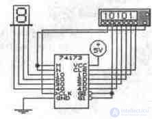
Fig. 9.40. Register inclusion circuit 74173
Register K155IR15 (74173) is a library component of EWB and can serve as an example of a storage device with three output states. The circuit of its inclusion is shown in Fig. 9.40. Note the extremely unsuccessful location of the findings of the register 74173 and their discrepancy with the original [7, 8]. As can be seen from fig. 9.40, K155IR15 - four-digit register. It has outputs 1Q ... 4Q with a third Z-state (with signal 1 at the terminals G2, G1), and its inputs 1D ... 4D are equipped with logic elements for writing permission by supplying a logical 0 to the inputs M, N (in EWB shown by lines). The register is used as a four-digit code source capable of serving directly the data bus of the digital system.
The information is loaded into the register synchronously with the positive difference of the clock pulse if low level voltages are present at the inputs M and N. If one of these inputs has a high level voltage, after the positive clock difference has arrived, the previous data should remain in the register. The CLR reset input is high active. If an active low level voltage is applied to the inputs G2, G1, the data contained in the register are displayed on the outputs 1Q ... 4Q, the presence of at least one high level voltage on the resolution inputs G2 and G1 causes a Z-state (open) for the output lines . Moreover, data from the registers does not pass the data bus of the systems, the outputs of the register do not affect the operation of other similar outputs connected to the bus conductors. The operation of the CLR and clock reset inputs does not affect the change of levels at the inputs.
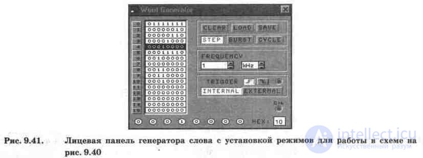
The K155IR15 register consumes a current of 72 mA and has a clock frequency of up to 25 MHz; Option 74LS173 consumes a current of 30 mA, its clock frequency is 30 MHz. The operating modes of the generator in the circuit in Fig. 9.40 and some code combinations are shown in fig. 9.41.
The second most common class of registers are shift registers, which are very diverse both functionally and in terms of circuit designs and characteristics. Shift registers, in addition to the storage operation, convert the serial binary code to parallel and parallel to serial, perform arithmetic and logical operations, and serve as time delay elements. They owe their name to the shear operation characteristic of these devices. With the arrival of each clock pulse, the contents of the trigger of each bit are rewritten (shifted) to the neighboring bit without changing the order of ones and zeros. When shifting information to the right after each clock pulse, the bit from the older bit is shifted to the lowest, and when shifting to the left, vice versa.
On domestic schemes, the letters RG are the register symbol. For shift registers, the shift direction is also indicated:> - to the right; <- to the left; <-> - reverse (bidirectional).
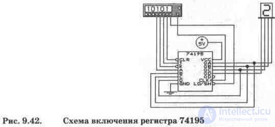
Let us consider the operation of the shift register using the library register 74195 (K155IR12) as an example, the switching circuit of which is shown in Fig. 9.42. IC 74195 is a high-speed register for performing shift, count, accumulation and mutual parallel-serial conversion of digital words. Parallel data is loaded through the LD / SH input and shifted to the right. If a high voltage is present at this input, serial data is entered into the register through the inputs of the first trigger J and K. Input J has a high active level, input K is low; if these inputs are connected, we get a simple D-input. Data is shifted in the direction from QA to QB, QC, and then to QD after each positive edge at the CLK clock input.
If a low (active) level voltage is present at the LD / SH input, all four register triggers are triggered by a single clock differential (from low to high). Then the data from the parallel inputs A ... D are transmitted to the corresponding outputs QA ... QD. Data shift to the left is provided in the circuit, where each output Qn is connected by an external jumper to the input Dni, i.e. switching circuit in fig. 9.42 corresponds only to the data reception and storage mode.
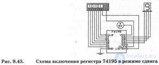
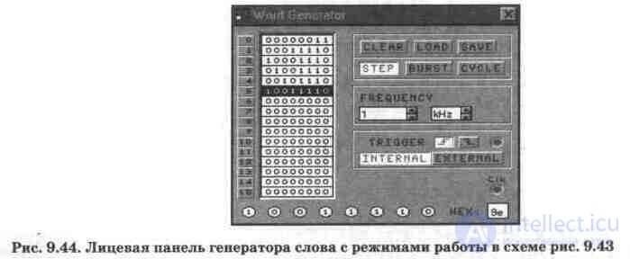
The scheme of switching on the IC in the shift mode is shown in Fig. 9.43, the modes of operation of the word generator are shown in Fig. 9.44. For the shift mode, the voltage at the LD / SH input must be fixed at a high level. Due to the fact that all operations in the register IR12 are strictly synchronous and it is triggered by the pulse front, the logic levels at the inputs J, K, Dn, LD / SH can be arbitrarily changed before the start of the trigger. Low at the input of the CLR, all output signals are set to low.
A low voltage at the input of the CLR also means a ban on the CLK clock; to correctly reset the data, you must choose the moment when a low voltage is present at the input of the CLK.
Test questions and tasks
1. What is a register, what functions can it perform?
2. What are the types of registers and their possible applications.
3. Conduct a simulation of register 74133 according to the diagram in Fig. 9.40. When modeling, it is necessary to select binary combinations of the word with the help of a generator, which allow you to check all modes of its operation. It is also advisable to compile a so-called state table that resembles a truth table [7, 8].
4. Simulate the register 74195 in the data reception mode (Fig. 9.42).
5. For the one shown in fig. 9.43 diagrams, examine the following shear modes [7]:
1 - shift and installation along the first cascade (JK = 11); 2 - shift and discharge along the first stage (JK = 00); 3 - shift and switching of the first stage (JK = 10); 4 - shift and storage in the first cascade (JK = 01). Moreover, as indicated above, CLR = 1, LD / SH = 1, the state of input A is indifferent.

Comments