
Lecture
Did your prototype fail at the worst possible moment? Did your device fail comprehensive testing at the customer's site? Did your mobile phone “glitch”, did the “telly” burn out after moving house, or did the air conditioner break down in the height of summer? Oh well, bad luck! Perhaps. But maybe the reason lies in an insufficiently worked-out circuit or design of the device, perhaps some key point was missed during development? If you have read the previous article “why equipment breaks down”, then you have probably already guessed … yes, that very same forgotten concept of “reliability”. This article by no means claims to fully cover such a broad topic as the design of radio-electronic equipment (REE), but in it I will try to shed light on. Design problems, typical design errors that lead to a potential (and in most cases real) reduction in the reliability of the equipment being developed. Having accumulated some experience in developing radio-electronic devices, I want to share it with fellow developers. Of course, seeing the “rakes” does not mean not stepping on them, everyone goes through their own “bumps”, but I think the ideas set out on these pages will find a response in the minds of many developers. Let's try together to figure out what “bad luck” really is and how to fight it.
As is well known, “luck” is a category belonging not so much to the “lucky” as to the persistent and hard-working. In this case that is exactly how it is, since the success of a development entirely depends on the responsibility of the approach to design, its comprehensiveness and breadth of coverage, and the determination and qualification of the developer. As already described in the previous article “Why Equipment Breaks Down, or What Is the Forgotten Concept of “Reliability””, reliability is a complex category, although it is expressed by a single, quite specific numerical parameter — the probability of failure-free operation. So, when designing, attention must be paid to all aspects affecting reliability indicators. The issues considered here echo those listed in the previous article. We will assume that the reader is already familiar with the previous publication. So, let's begin. To avoid getting confused, let's try to divide the whole “space of problems” into categories (in brackets the connections with the problems described in the previous article will be indicated):
1. Organizational aspects
2. Circuit design aspects
3. Construction aspects
4. Software problems
5. Design problems
6. Testing tasks
7. Preparation of design and user documentation
Let us leave many organizational problems outside the scope of this article and concentrate on one — the most important for the developer — the technical specification (TS). For some, this abbreviation inspires horror, some, seeing it yet again, wave it off like an annoying fly, and some treat it with full responsibility and as “the natural order of things”. But, be that as it may, everyone has to deal with a TS in one form or another. A complete TS is a complex, multi-page document, largely individual for each development. It is possible that there is no such thing as a universal TS at all, but there are still basic points that are worth adhering to when drawing it up. It is known from experience that somewhere in the middle of the path to completion of the work, seditious ideas begin to arise that everything should have been done completely differently. It happens that the TS is repeatedly refined and agreed upon over the course of the work, and, as a rule, one of “Murphy's laws” is confirmed: “Only at the end of the work do we usually find out how we should have started”. But nevertheless, the TS allows you to choose the right direction of activity, determine deadlines and “checkpoints”, soberly assess the volume of work and distribute forces. And therefore, being the basic document for the start of the work, the TS requires close attention. It must be remembered that the TS is a document both from the customer to the developer and from the developer to the customer. Drawing it up is a mutual and iterative process. In the course of drawing up the TS, it is necessary to clarify all disputed points, otherwise agreeing on these points with the customer at the stage of completion of the work can easily turn into a legal matter. The absence of a TS in development is akin to the absence of a contract in civil law. Drawing up a competent TS is a whole art, but many neglect even its simplified version, and in vain. To be able to assess the importance of this document, I will give the typical items of a TS.
— Requirements for characteristics
— Reliability requirements
— Operating conditions
— Special requirements
Drawing up a TS, as I have already said, is beyond the scope of this article. Those interested can be advised to study the relevant regulatory documents, as well as to visit thematic sites devoted to the development of design documentation.
So: the TS is ready, what next? Now, on the basis of this TS, the developer must draw up for himself (and for the customer too) a “work plan”. The plan should contain approximate deadlines for completing key stages of the work, deadlines for presenting intermediate control results, and of course the deadline for completion of the work. In the interval from the start of the work to the delivery of the result, the developer is free to vary the deadlines of intermediate stages, however, a large deviation from the assigned deadlines at checkpoints is an alarming signal. In practice, of course, it is rarely possible to meet the specified deadlines exactly, but at least one must strive to stay within the allotted time frame. So there is no way without a plan, otherwise the development risks dragging on for an indefinite time. The problems mentioned above are usually absent in “grown-up design bureaus” (but where are they now?) and, as a rule, appear in small teams, in private enterprises, which now make up the majority. But even with a TS and a work plan in place — the most typical and dangerous mistake — is underestimating the development timeline. The reasons why this happens are completely different, from simple underestimation of difficulties to the desire to offer the customer more favorable terms of cooperation. The result is the same — work under time pressure and, in the end, missed deadlines and deteriorating quality of work. If the developer does not have at least a few major projects behind him (on which at least six months of work was spent), then one can safely multiply the seemingly reasonable development deadlines by 1.5 or even 2. “Well, that's too much!” you think? Analyze all the “bottlenecks” and “slippery” spots in the TS and you will almost certainly agree. Don't rush — better take an extra day to think it over. More experienced developers make mistakes in estimating deadlines much less often. Well then: the TS and the work plan are ready, now we can get down to the most interesting part.
What does the construction of a building start with? That's right, with the foundation. Well, for a schematic diagram, the foundation is the block and functional diagram. While most specialists really do have sufficient qualifications not to make mistakes in individual nodes and stages of a schematic diagram, on the whole, in the absence of a block diagram, the developer often moves in a non-optimal direction. Having a block diagram allows you to begin designing the device at the “upper level of the hierarchy”, to see its fundamental strengths and weaknesses. Whereas its absence often “fixates” the developer on “particulars”, preventing the creation of an optimal structure for the device. And furthermore, the absence of a block diagram can significantly complicate modification of the development, failure analysis and repair. Try, for example, to describe the operation of a complex technical system (say a PC) without dividing it into functional blocks. It's unlikely to work out, and even if it does, we still willy-nilly operate with macro-concepts: “chipset”, “processor”, “bus”, etc. That is, we structure a complex system. This is quite natural. But for some reason, during development, the structural representation of the device being developed is often completely ignored. “Dumping everything into one pile” is still possible while running the project (although there will surely be mistakes due to lack of an overall vision), but after some time has passed, it can be very hard to sort out such a “mess” without a detailed description and a block diagram. And analyzing such circuits is extremely, extremely difficult (especially if it is carried out not by the author of this development, and moreover in the absence of an explanatory note). The only excuse for the absence of a block diagram may be, in my opinion, only the simplicity of the project (it would be silly to draw a block diagram, for example, for a simple power supply).
The functional diagram is no less important. Let's clarify the concepts of functional and block diagrams, since many do not see the difference between them. A block diagram should represent the device as complete functional blocks, show the relationship between them and reflect the general operating principle of the whole device. Looking at a block diagram, even a beginning specialist familiar with the basics of the subject should understand how “it” works. If there is no such understanding, then it can be said that such a block diagram is no good. A functional diagram is a more detailed diagram of functional units (possibly even with elements of a schematic diagram). A functional diagram reveals the operating principle of a functional block or unit. It is, so to speak, a lower level of the hierarchy than the block diagram, but is not yet a schematic diagram.
Precise block and functional diagrams, like a precise TS, as a rule, can only “be born” after the completion of development, but this does not prevent creating them in a “first approximation” at the very start of the work. These diagrams will accompany you throughout the whole time of work on the project (and even afterwards, when searching for errors and analyzing failures). So I recommend taking this very, very seriously.
To give the reader an opportunity to stretch his mind and be convinced of this, let us consider some non-trivial, complex project, for example a robot (fig.1).

Fig.1. Example of a block diagram of a complex technical system (a robot)
Analyzing this block diagram, one can without much difficulty see the weak and unreliable spots, and also understand the potential capabilities of the system, assess the labor intensity of designing each functional unit, etc.
A block diagram makes it possible to clearly see the interrelation of all the structural links of the technical object being designed. It always allows you to assess their mutual influence and importance, which is especially valuable in the structural analysis of system reliability, since firstly: it allows you to see “bottlenecks”, the presence and influence of destabilizing factors, and secondly: to make adequate corrections to the structure of the system. The same applies to functional diagrams, but at a more detailed level. A block diagram often makes it possible to divide the project into “separate” sections, and to assign work on them to different engineers or groups. In addition, a block diagram allows you not to get confused in a complex project and not to fall into time pressure, competently distributing forces and time. Every developer has gone through situations in his life of working under conditions of time shortage, when forces were thrown “in the wrong direction”, and now, when deadlines are tight, one has to “rush” the work, making a mass of mistakes along the way. As a rule, this ends in nothing but loss of nerves, health and the customer's trust. But let us assume that we have coped with creating the structure of the system being designed and with the functional diagrams, now it is required to “pack” this skeleton with “flesh”.
Schematic diagrams can be regarded as the lowest level of hierarchy of diagrams of any kind (including block and functional diagrams). The overall schematic diagram is naturally a combination of the schematic diagrams of the functional units and blocks. We will not talk about classic circuit-design errors, assuming that the developer is qualified enough not to make them. By the way, one should always remember one of “Murphy's laws”, which states: “a qualified specialist successfully avoids minor mistakes, steadily moving toward some global misconception”. This is relevant to the discussion of the block diagram. Knowledge of the fundamentals of circuit design by no means ensures the optimal construction of the system structure as a whole. It is not for nothing that there are two specialties with similar names — “circuit designer” and “systems engineer”. In modern conditions, these two specialties are often combined in one specialist, who does not pay due attention to systems engineering. Remember: if you have encountered any insurmountable technical difficulties, then perhaps it is worth reconsidering the block diagram. The wisdom is always confirmed: “if something isn't working, it means you are doing the wrong thing, or doing it the wrong way”.
We begin “sculpting” the schematic diagram. So: the developer has up-to-date information on modern components and technologies, has a block diagram in front of him, and his qualification is sufficient to embody all this “in metal”. But here too a “little devil” is lying in wait, nudging “his elbow”. Here are the typical omissions at this stage of development that, as a rule, lead to a reduction in reliability.
Incorrect interpretation of RC parameters from reference data
Many RC manufacturers, for advertising purposes, give on the title pages of the technical documentation for the RC the maximum achievable, best parameters. And many developers use precisely these parameters, forgetting to check under what conditions they are achievable. And besides the best there are also the worst. Who said you got hold of a component with the best characteristics? A good rule — always proceed from the worst-case RC parameters. It happens that the developer completely ignores such non-obvious parameters as the permissible power dissipation of the RC's package, the permissible voltage for resistors or the permissible current for capacitors. For some it is also a revelation that besides the average power there is also a peak power, which is likewise regulated. Some manufacturers invent their own names for characteristics, so what to do then? There is one piece of advice — read the documentation carefully, think through the physical meaning of the parameters, and be guided by common sense.
Ignoring reliability indicators and “abusing” RCs in extreme operating modes
Often the reliability calculation of a product is not done at all, but this is not the worst thing, since, if simple rules are observed, in most cases the reliability indicators of the whole product will be quite satisfactory (based on the reliability indicators of the RCs). After all, RCs are designed to work in “normal” conditions and have quite good reliability indicators when doing so. The task is not to go beyond the boundaries of the “normal” operating conditions of the RC, and then everything will be fine. Of course, this does not apply to mission-critical developments, where failures can lead to catastrophic consequences and a full reliability calculation is mandatory. By the way, it happens that the data needed for a full reliability calculation is quite difficult to find, since few manufacturers publish these parameters in standard “datasheets”. In this case, too, observing a number of simple rules allows you to be sufficiently confident in the reliable operation of the unit being designed. From my point of view, these rules go as follows:
Some may object that all this is an “anachronism”, that this is how things were done in the days of the Soviet Union, and now RCs work perfectly well even at 100-150 °C. Sure, and “…the number “π” in wartime can reach a value of 4”, only the laws of physics don't know about that. And the formulas for calculating “λ” are the same as they were 20 years ago. So I would still recommend adhering to the simple rules given above.
For example, for semiconductor devices, the failure rate as a function of temperature, applied voltage and current is approximately expressed by the formula:
λ(Tj, U, I) = λ(Tjmax, Umax, Imax) x (U / Umax)2 x (I / Imax)2 x exp[–B x (1 / Tj–1 / Tjmax)]
It is easy to notice that the failure rate “λ” doubles every 20 °C and has a quadratic dependence on U and I. That is, when the applied voltage (U) or the flowing current (I) is reduced by half, “λ” drops by a factor of 4. Observing the rule of loading REs to no more than 75% provides a reduction in failure rate of more than 3 times! Lowering the temperature reduces the probability of failures of all kinds, and also reduces the degradation of RE parameters over time. Reducing the operating voltage is especially relevant for high-voltage devices, since it significantly reduces the probability of electrical breakdown, while reducing currents is relevant for high-current devices, since it hinders the degradation process of metallizations and contact joints. Of course, this is not dogma, and there are exceptional cases where such rules are not applicable, but the trends are clear.
Circuit simulation errors in systems such as “PSpice”, aggravated by insufficient engineering calculations
Among colleagues one comes across three kinds of engineers. The first naively believe that circuit simulation systems can do everything. The second, on the contrary, do not trust them at all, and the third reasonably use such systems, drawing on common sense, theory and a healthy dose of skepticism. Of course, circuit simulation systems such as “PSpice” are not a panacea, but they are a very powerful tool in skilled hands. And here it is necessary to understand that there are a number of conditions that must be remembered and observed.
First: there is a finite precision of machine computations, and a finite precision of numerical mathematics algorithms, which is especially noticeable when analyzing transient processes. By “cranking up without knowing” the simulation parameters, one can obtain absolutely absurd results, I repeat, especially in transient processes.
Second: the correctness of the calculation is also determined by the correctness of the supplied input data. This applies both to the schematic diagram used for the simulation and to the mathematical models of the REs, and here, unfortunately, the desired completeness and reliability of the input data is far from always attainable. The circuit used for simulation may differ from the real circuit, for example, by introducing fictitious resistances, negligibly small ones, connected in series with an RE, or negligibly large ones, connected in parallel with certain circuit nodes. Mathematical models of REs may fail to account for all of their parameters. The most correct approach is to use the mathematical models provided by the RE manufacturers, but even in this case full reliability of the simulation cannot be guaranteed.
Circuit simulation systems are complex programs, and one must know how to use them. Even a qualified specialist is not always able to correctly simulate certain circuits. In such cases I always recall the winged phrase “not knowing is not shameful, not learning is shameful”. Today there is a wealth of literature on the theory and practice of simulation in systems with a “Spice” computation engine, but nevertheless it is not always possible to reliably calculate the behavior of a circuit.
To sum up, I will say that simulation systems are a powerful tool in the hands of a circuit designer, but they require careful handling, competent preparation of the input data and interpretation of the results. It is advisable to make an approximate “by-hand” analysis in order to protect oneself from obvious blunders. It never hurts to understand what exactly we are trying to simulate, and what the expected result is. And here “hoping for the best” does not work either, otherwise engineering analysis turns into a sham. In principle, any CAD system requires careful attention. Many CAD systems (including programming environments) have both amazing development capabilities and an amazing capacity for allowing extremely insidious errors (owing to their complexity). If one is really going to use the tool, it is necessary to study it as thoroughly as possible.
Underestimation of the EMC of the device's units and assemblies, and of the influence of interference and destabilizing factors in general
Why filtering capacitances, limiting circuits, stabilization of “operating points”, and so on? It will all work anyway… Of course it will — but only under “greenhouse” conditions. Even small external influences are in most cases capable of disrupting the normal operation of such units, not to mention intense interference, temperature stresses, and simply the effect of time. Questions of EMC and the influence of destabilizing factors naturally fall away for developers of precision analog and power electronics, since without taking this into account, most of the circuits would simply be inoperable. Today a very large number of engineers deal with digital technology, where these issues are not as relevant, and moreover the abundance of analog (including precision) highly integrated microchips allows many circuit units to be designed simply by using standard circuits from “datasheets”. Unfortunately, many engineers refuse to look beyond “datasheets” and forget the very basics of analog circuit design. Of course it is convenient to build a circuit “out of building blocks”, but even the most modern microchips require at least some supporting circuitry, and in a number of cases additional to the standard one (for example, limiting circuits at inputs and outputs, power filters, buffer stages). This is exactly where an engineer who is shaky in matters of analog circuit design and EMC makes mistakes. Their danger lies in the fact that they rarely manifest themselves, and are therefore hard to eliminate, and moreover the developer's insufficient qualification often allows them to “take root” in the product, if not forever, then for a long time.
As for destabilizing factors, it must always be remembered that things such as changes in operating conditions within the technical specification (fluctuations of temperature, humidity, pressure, mechanical loads, etc.) must not lead to system failures or a degradation of its characteristics to unacceptable values. Temperature and time drifts of RE parameters, degradation of characteristics, etc., must also not be left unattended. The possible effects of electromagnetic and electrostatic fields, induced and conducted interference, and mechanical loads should be analyzed. These effects can be either generated by the system itself or act from outside. In any case, destabilizing factors must not disrupt the normal functioning of the product.
Neglect of physical phenomena in the RE and in the system as a whole
Continuing the topic touched upon in the previous paragraph, I will say that neglect of physical phenomena in the RE and in the circuit as a whole, as well as ignorance of their influence, presents the developer with a great many surprises. So that the matter does not seem simple, let me just list some of them:
Effects in semiconductors (Miller, Early, critical rates of rise of voltages and currents, etc.), the capacitance and inductance of the mounting (including of the printed circuit), the capacitances and inductances of leads and other parasitic parameters of REs, the temperature gradient on the printed circuit board (especially important for precision circuits), the temperature coefficients of RE parameters, wave effects in the HF/microwave range, as well as electromagnetic compatibility (EMC) problems, permissible current densities for conductors and printed-board traces, the voltage drop across conductors (even copper has resistance), the thermo-EMF of junctions, the aging of materials and REs, degradation of their characteristics (especially under high-temperature conditions), time and temperature drifts of op-amp parameters, the influence of humidity, dust and temperature in power and high-voltage circuits, surface breakdown, ionization of air and polarization of dielectrics, etc. It is also worth remembering the physical properties of materials: thermal conductivity, heat capacity, hygroscopicity, strength characteristics, mechanical stresses in the REs and structures across the entire operating temperature range.
And this list is still not complete. So what should one do? Well, first, not all of them occur in any given specific circuit. And second, it is necessary to identify the most critical units in the circuit (for example: precision, power, high-voltage, etc.) and then consider the possible physical phenomena for them specifically. Solving these problems comes more easily to a developer with experience and a broad outlook, but, unfortunately, experience accumulates very slowly.
Absence of “what if…”-type analysis
An intriguing opening, isn't it? Yes, this is not a “Monte Carlo” type analysis or another “classical” one, this is, so to speak, an analysis of “improbable” situations. But are they really so improbable? Let me give some examples: Look at the circuit fragment shown in Fig.2. Now imagine that the microcontroller (MCU) has hung, and its pins are in a “Z” state or have been reprogrammed as inputs. What will happen to the transistor then? But if the node had been slightly modified, as in Fig.3, nothing would have happened.
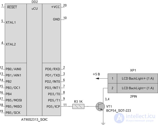
Fig. 2. Dangerous circuit for connecting a transistor to the MCU (potential "floating base")
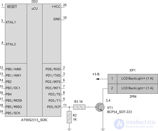
Fig. 3. Safe circuit for connecting a transistor to the MCU
Here is another example. Look at the circuit of a capacitor-dropper mains power supply in Fig.4, and now imagine what will happen to the elements if the shape of the supply voltage differs from a sinusoidal one, for example due to surges in the mains or “chatter” in the connector block or in the plug-socket pair?
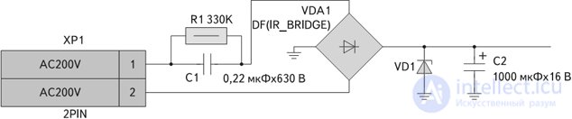
Fig. 4. Example of a circuit that does not account for probable switching overloads and surges in the supply mains
Agree — these are not such “improbable” situations after all. Of course, the circuit “acquires” overvoltage protection elements and becomes quite expensive to implement, but it is much more correct to do things “the way they should be done”. Many such examples could be given. Moreover, this should also include an analysis of “improbable” user actions, for example: pressing all control buttons simultaneously, inadequate action situations, forced power shutdown, etc. Why? Well, the user just felt like doing it, physically it is possible after all. In circuit design, too, protection is needed against an “inventive” or unqualified user. Let me formulate some types of analyses carried out for “improbable” situations:
1) Analysis of circuit operation when programmable or software-configurable elements are removed from it. In this case all remaining REs of the circuit must operate in normal modes, there must be no “floating” bases and gates, no unacceptable voltage surges, etc.
2) Analysis of circuit operation when the functions of bidirectional programmable pins change (for example, microcontroller (MCU) ports). Look at the circuit fragment in Fig. 5 and 6 and imagine that the MCU inputs have been reprogrammed to operate in “output” mode.
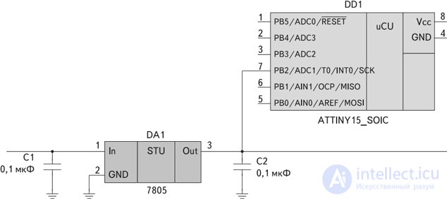
Fig. 5. Circuit leading to overload of the MCU port in the event of a software fault
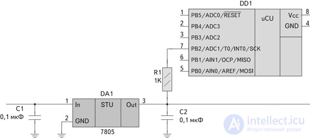
Fig. 6. Use of a protective resistor at the MCU input (protection against overload of the MCU input in the event of a software fault)
What will become of them? Adding an extra resistor costs practically nothing. In general, any bidirectional ports should be treated as output ports (i.e., switching these ports to output mode with an arbitrary setting on them of either logic “0” or logic “1” must not lead to overloads of the circuit elements). If you pay special attention to the reliability of the device, then it is worth carrying out such an analysis, since the reliability of an MCU or another processor is closely tied to its firmware, which is often not distinguished by stability of operation. For the same reasons, the circuit shown in Fig.8 is more preferable than the one shown in Fig.7.
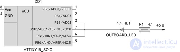
Fig. 7. Example of an undesirable parallel connection of MCU output ports (overloads possible in the event of a software fault)
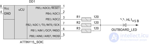
Fig. 8. Safe circuit for "paralleling" MCU output ports
3) Analysis of transient processes under a step change of input signals (including supply voltages) and loads (including open circuits and short circuits). The simplest and most illustrative method is to replace all capacitances with jumpers (or voltage sources with the EMF “before the transient process”), and all inductances with open circuits (or current sources with the currents “before the transient process”). It should be remembered that during a transient process “current surges” flow through a capacitance and the capacitance itself is treated as a short circuit (recall the properties of a voltage source), while “voltage surges” appear across an inductance and the inductance itself is treated as an open circuit, i.e. a break (recall the properties of a current source). By making such a substitution, you will easily see the elements subject to overloads.
4) Analysis of circuit and firmware operation under abnormal situations. For example: ensuring data integrity in the event of a sudden power loss during active exchange with non-volatile memory, the adequacy of the system's response to incorrect user actions, etc. I agree that it is impossible to foresee everything; here, as they say, one will have to rack one's brains hard.
5) Analysis of circuit operation under the worst operating conditions provided for by the technical specification, moreover when all the conditions are worst simultaneously.
6) It is always useful to carry out a “static” survivability analysis, “acting” on the inputs and sometimes also the outputs of the circuit with kilovolt pulses, for example from a human body model (series-connected RC 1.5 kOhm/100 pF ±10 kV). This often reveals weak points whose circuit design it may be worth reconsidering. As is well known, the effect of “static” is one of the most frequent causes of equipment failure, which is especially relevant for devices intended to work with a human operator, as well as those operating under industrial conditions, where the accumulation of static electricity charges is possible.
In conclusion, I will add to this section a number of simple rules that make it possible to significantly increase the reliability of circuit operation and make them easier to understand.
The range of structural design questions is very wide. It is practically impossible to fully answer them within the scope of a journal article. I will touch on only the most “popular” ones.
The printed circuit board can be considered the “bridge” from the electrical circuit to the mechanical design, being a kind of “fusion” of the electrical circuit and the mechanical structure. It is precisely the printed circuit board that determines the mechanical strength of the electronic assembly mounted on it. In a number of cases it serves as one of the load-bearing elements of the entire device's structure. In many respects, it is precisely the printed circuit board that is responsible for the EMC and thermal conditions of the REs. In general, the printed circuit board is an extremely important link in the product being developed, and many structural reliability questions are directly or indirectly connected with it.
One of the determining elements of the reliability of an assembled printed circuit board is the footprint (land pattern) of the components. A correctly designed footprint (taking into account the soldering and assembly technology and the spread of component dimensions) will ensure a minimum of defects during product assembly. In my own practice, when designing footprints, I prefer to be guided by the IPC-7351 standard. A good aid in this is the “freeware” program “PCB Matrix LP Viewer” (http://www.pcblibraries.com). In any case, it is advisable to coordinate this issue with the designers and process engineers of the assembly production, who will give the necessary recommendations on tolerances and clearances (for example, for an automatic placement operation). Nor should the question of proper footprint marking be lost sight of. The necessary information in the marking (silkscreen) layer will significantly simplify the process of assembly, repair and maintenance — for example, information about the component outline, pinout (marking of key leads), reference designator, and explanatory labels at connectors, test points and trimming elements.
When designing the footprint of massive components, one should not forget about the need for their additional fastening. This significantly increases the reliability of the printed circuit assembly under mechanical overloads (shocks and vibration). Designers quite often consider additional fastening of large components unnecessary, despite the manufacturer’s recommendations for the component. I myself, for example, have more than once seen components that had literally shaken loose from boards in equipment operating under heavy vibration loads. In this connection I want to say that the choice of the printed circuit board’s mounting points is also important. Rarely does an engineer perform a strength analysis (including a modal analysis), despite the fact that modern CAD and FEM packages allow such an analysis (at least an estimative one) to be carried out even by an engineer of average qualification. In many cases it is even sufficient to lay out the arrangement taking into account possible shock and vibration loads, relying on experience, rough calculations and common sense, although, of course, subjective criteria are sometimes far from objective ones. Incidentally, for equipment operating under significant mechanical overloads, it may be worth reconsidering the component base, giving preference, for example, to components with better mass-and-size characteristics (which naturally also have lower moments of inertia, which favourably affects the vibration resistance of the electronic assembly).
The process of designing a printed circuit board is also inseparably linked with the question of layout, which is also connected with the design of the product. One often encounters layout flaws such as: an unfortunate placement of components, heat sinks, connecting terminals and interface connectors that hinders assembly or repair work, violates process clearances (for example, for high-voltage circuits), creates an unfavourable thermal regime in the device once it is assembled in its enclosure, and so on.
Particular attention should be paid to ensuring a normal thermal regime for the components in the assembled device. Optimal placement of elements on the printed circuit board makes it possible to avoid many unpleasant effects, for example a temperature gradient (which is especially important for precision assemblies). The example shown in Fig. 9 shows how a temperature gradient caused by an unfortunate layout can lead to degraded circuit characteristics. The difference between elements R3 and R4 reaches 20 °C, which for general-purpose resistors means a resistance drift from the nominal value of several percent.
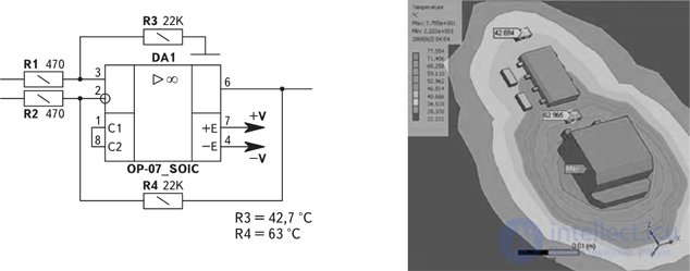
Fig. 9 A layout leading to malfunction of a precision circuit due to a temperature gradient on the printed circuit board.
Fig. 10 shows the “local overheating” effect, when heat-generating elements placed close together on the board “warm each other up”, producing a local concentration of substantial thermal power with unsatisfactory heat removal. To get out of this situation it is enough to ensure a more even distribution of heat, for example by “spreading apart” the heat-generating elements over greater distances.
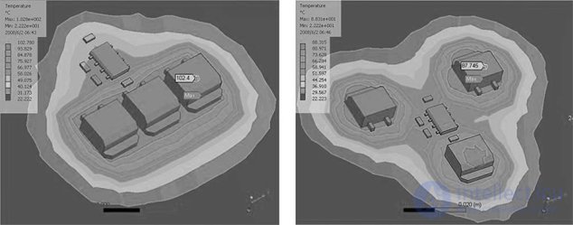
Fig. 10 An example of a layout leading to local overheating of the printed circuit board and components, and an example of a layout providing an easier thermal regime.
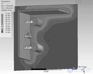
The “greenhouse” effect shown in Fig. 11 guarantees overheating of the zone “inside” the heat sink due to absorption of thermal radiation by the components located there, and also due to insulation of the convection flows.
 |
|
Fig. 11 An example of a layout that is unfortunate from the standpoint of heat removal |
One could cite dozens more unfortunate layout examples from the standpoint of ensuring thermal regimes. This only shows how individual each design decision can be, and that no universal recommendations exist here. One need only bear in mind the possible “pitfalls” and pay careful attention to the issue of ensuring the thermal regimes of the assembly.
No less important than ensuring thermal regimes is the question of electromagnetic compatibility (EMC). Here the expression “prevention is better than cure” fits better than anywhere else. It is better not to fight interference, but not to create favourable conditions for its occurrence in the first place. The best way to combat pulsed and RF interference is to localize the circuits that generate the interference — as a rule these are circuits carrying pulsed and RF currents of significant magnitude (“significant” being a purely subjective notion, individual to each specific design). A good method is to minimize the traces on the printed circuit board and the connecting wires for circuits carrying pulsed and RF currents, as well as to shunt with decoupling capacitors on the power supply those parts of the circuit that consume large pulsed power. If it is not possible to localize the source of interference, then the circuits and parts of the circuit susceptible to interference must be protected. As regards low-current and precision circuits, there are a number of methods described in the literature. Another effective method of protection against interference is shielding. One can shield either the source of the interference or the sensitive parts of the circuit affected by the interference. Shielding may be implemented both by screens (electromagnetic and electrostatic) and by structural elements, as well as by ground planes (polygons) and special layers on the printed circuit board.
The next important point, especially for high-current, pulsed and precision circuits, and in the hardest case a combination thereof, is the routing of the “power” and “ground” traces. Often insufficient attention is paid to the routing of these circuits, and as a result the reliability of the circuits drops sharply, the probability of malfunctions in operation increases, and the characteristics deteriorate, up to complete inoperability of a product that worked successfully “on the breadboard”.
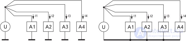
To ensure proper routing of the “ground” and “power” circuits, it is necessary to identify the functional blocks of the circuit that consume large currents, as well as blocks that are sensitive to power-supply interference. Having identified such sections of the circuit, the power and “ground” traces must be routed in such a way as to produce independent loops for the supply currents flowing to each block. In doing so, the “grounds” of all the blocks, as well as of the common power source, must be equipotential, both for direct current and for RF (for pulsed circuits one can be guided by the frequency of the 3rd, or better the 5th, harmonic of the shortest pulse signal). Structurally, equipotentiality is usually achieved by routing the “ground” with traces of minimum length and the greatest possible cross-section. As an example, let us consider the topology shown in Fig. 12.
 |
|
|
Fig. 12 Theoretically correct scheme for separating the supply-current loops |
Fig. 13 Scheme for separating the supply-current loops taking into account the real, non-zero impedance of the "ground" bus |
If the “grounds” of all the blocks “A1”…“A4” and of the power source “U”, with a negligibly small internal resistance, are equipotential, then the currents “I1”..“I4” in the supply loops will in no way affect one another. In practice, implementing this topology can be difficult; in particular, it is problematic to ensure the equipotentiality of the “grounds” of all the blocks. As a rule, the real circuit looks approximately as shown in Fig. 14, i.e. there is some “ground bus” with a non-zero (possibly even quite large) impedance. The designer’s task is to reduce its impedance to a minimum.
In addition to reducing the inductance and ohmic resistance of the conductors and printed traces by varying their “geometry”, a fairly effective, well-known means of reducing the RF impedance is the use of decoupling capacitors on the power supply, which make it possible to level out these parasitic parameters. By excluding the flow of pulsed currents through the power and “ground” traces, we thereby prevent these conductors from working as “antennas” that transmit interference. This is achieved, as I said above, by means of a competent topology and the use of decoupling (in this case one could say “reservoir”) capacitors on the power circuits. The term “reservoir” is more appropriate for capacitors placed in the immediate vicinity of the nodes that consume large pulsed currents, where the node is powered precisely from the energy stored in the capacitor, thereby excluding the flow of pulsed currents through the long supply and “ground” traces.
If the blocks are connected by analogue signals relative to a common “ground”, then the variant with equipotential “grounds” is, of the feasible options, the only simple one. As an alternative, it is possible to build a circuit with galvanic isolation on the control signals, but for analogue systems this leads to a serious complication of the circuit design. For digital systems, in most cases, galvanic isolation is done much more simply.
If the blocks are independent, or some of them are dependent, then the task is significantly simplified. In this case one can, as shown in Fig. 15, make only the “grounds” of the connected (dependent) blocks “A2” and “A3” equipotential, or separate the supply loops, providing each block with a decoupling (reservoir) capacitor, and connect the dependent blocks by a galvanically isolated channel, as shown, for example, in Fig. 16.
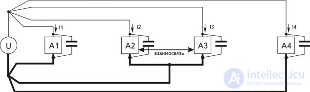
Fig. 14 An example of a combined "ground" routing topology (equipotential and "independent" "ground" nodes)
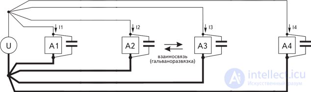
Fig. 15 An example of a routing topology with "independent" "grounds" and a galvanically isolated channel interconnecting the blocks
Another way of solving the problem of power-supply decoupling — the use of a low-pass filter, as shown in Fig. 17 — is more complex to implement, but sometimes also more effective, allowing in some cases the power routing to be simplified (it is more often used in RF circuits); true, in this case the problem of ensuring the equipotentiality of the “grounds” also arises. In practice it is often necessary to apply both methods (the truth, as usual, lies somewhere in the middle).
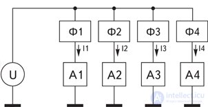 |
| Fig. 16 An example of a power-circuit routing topology with filters |
Generally speaking, practically all measures for improving EMC are aimed at minimizing the lengths of the traces along which pulsed and RF currents flow. It can also be said that the optimal solution is to localize these currents within loops of minimum size, formed by the components of the block and the mounting elements.
Summarizing the above, one can recommend doing at least approximate engineering calculations. Calculate the maximum possible overloads on the elements, analyse the printed circuit board layout from the standpoint of EMC and of ensuring the thermal regimes of power components and precision assemblies. Check the routing of the “ground”, power, precision and high-impedance circuits. It is necessary to assess the susceptibility of precision and high-impedance circuits to induced interference. We consider a circuit to be precision when the magnitude of the voltages or currents in it is six or more orders of magnitude smaller than their absolute values elsewhere in the given circuit. We consider a circuit to be high-impedance when the modulus of their total impedance is tens of kilohms or more (as a rule these are the inputs of analogue stages, op-amps, ADCs and the like). The circuit needs to be analysed for resistance to conducted interference on the inputs/outputs and other external-connection circuits. It also would not hurt to check the product’s resistance to shock and vibration — in case of doubt, carry out at least an approximate static and modal analysis, of course if there are corresponding requirements in the technical specification. Nor should one lose sight of matters related to assembly (verification of footprints, printed circuit board marking, fastening of massive components), as well as matters linking the layout of the product and its design.
In view of the fact that there is a vast multitude of programmable components, it is impossible to give universal recommendations suitable for all cases and for all programmable components; however, one can organize one’s work in such a way as to simplify debugging, error hunting and the future modification of programs as much as possible. Personally, I do not remember a single case where a program, once written, was never improved or modified, since, as is well known (from those same unforgettable “Murphy’s laws”), “every useful program contains bugs”.
Without claiming to hold the ultimate truth on “how a programmer ought to work”, I give below rules that have more than once helped me to effectively solve and prevent problems arising during the development, debugging and modification of software.
In programming there exists the following opinion — “the best comment on a program in a little-known language is a program in a known language”. Well then — the language that each of us commands to perfection is the natural language of human communication. Therefore the first and most important rule in programming is always not to be lazy about commenting the source text. Moreover, never put it off “for later”, for many ideas embodied in code, as ideas, are very quickly forgotten, leaving only the bare code, and understanding the essence of the program afterwards can be very difficult. Thus, the comment must be an inseparable part of the program and must be written simultaneously with it. So that writing a comment is not perceived as needless routine, let me offer a couple of thoughts on how I usually do this.
1) It is always necessary to place a block comment in the header
продолжение следует...
Часть 1 How to Ensure the Reliability of Radio-Electronic Systems
Часть 2 5. Design Problems - How to Ensure the Reliability of

Comments