
Lecture
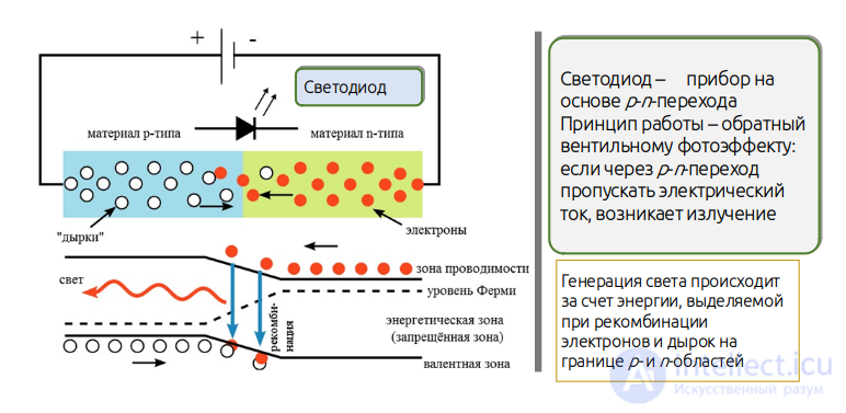
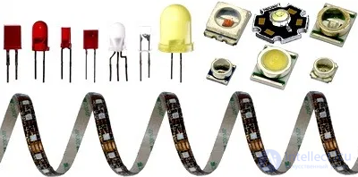
An LED (light-emitting diode) is a semiconductor emitting device with one or more electrical junctions that converts electrical energy into the energy of incoherent light (electromagnetic) radiation. LEDs are used in optical communication lines, modulators, indicator devices, optocouplers, etc.
The operating principle of semiconductor emitting devices is based on the phenomenon of electroluminescence, associated with the spontaneous radiative recombination of charge carriers injected through a p-n junction. The radiation is caused by nonequilibrium carriers and is concentrated in the p-n junction and the regions adjacent to it.
Schematic symbol

Oleg Losev, a Soviet physicist who discovered electroluminescence in silicon carbide
The first known report of light emission by a solid-state diode was made in 1907 by the British experimenter Henry Round[en] of Marconi Labs[en]. Round was the first to discover and describe the electroluminescence he observed while studying the passage of current in a metal — silicon carbide (carborundum, SiC) pair, and noted yellow, green, and orange glow at the cathode.
These experiments were later, independently of Round, repeated in 1923 by O. V. Losev, who, while experimenting at the Nizhny Novgorod Radio Laboratory with a rectifying contact made of a carborundum — steel wire pair, discovered at the point of contact of the two dissimilar materials a faint glow — electroluminescence of a semiconductor junction (at that time the concept of a «semiconductor junction» did not yet exist). This observation was published, but at the time the significance of this observation was not understood and therefore was not investigated for many decades.
Losev showed that electroluminescence arises near the junction of the materials/ There was no theoretical explanation of the phenomenon at that time. Losev fully appreciated the practical significance of his discovery, which made it possible to create small-sized solid-state (vacuum-free) light sources with a very low supply voltage (less than 10 V) and very high speed of response. He obtained two author's certificates for a «Light Relay» (the first filed in February 1927)[
In 1961, James Robert Biard (English)Russian and Gary Pittman of Texas Instruments discovered the technology of the infrared LED based on gallium arsenide (GaAs). After obtaining a patent in 1962, their industrial production began.
The world's first practically applicable LED, operating in the visible (red) range, was developed by Nick Holonyak at the University of Illinois for General Electric in 1962. Holonyak is thus considered the «father of the modern LED». His former student, George Craford (English)Russian, invented the world's first yellow LED and improved the brightness of red and red-orange LEDs by a factor of 10 in 1972. In 1976, T. Pearsall created the world's first high-efficiency, high-brightness LED for telecommunications applications, specially adapted for data transmission over fiber-optic communication lines.
LEDs remained extremely expensive up until 1968 (about $200 apiece), which limited their practical application. Research by Jacques Pankove at the RCA laboratory led to the industrial production of LEDs; in 1971 he obtained the first blue LED . The company «Monsanto» was the first to organize mass production of LEDs operating in the visible light range and applicable in indicators. The company «Hewlett-Packard» succeeded in using LEDs in its early mass-produced pocket calculators.
In the mid-1970s at the A. F. Ioffe Institute, a group led by Zhores Alferov obtained new materials — semiconductor heterostructures, currently used for creating laser diodes and LEDs . After this, mass industrial production of LEDs began. The discovery was awarded the Nobel Prize in 2000 . In 1983, Citizen Electronics was the first to develop and begin production of SMD LEDs, naming them CITILED .
In the early 1990s, Isamu Akasaki, working together with Hiroshi Amano at Nagoya University, as well as Shuji Nakamura, who at that time worked as a researcher at the Japanese corporation «Nichia Chemical Industries», invented the technology for manufacturing the blue LED (LED). For the discovery of the inexpensive blue LED, the three of them were awarded the Nobel Prize in Physics in 2014[10][11]. In 1993, Nichia began their industrial production, and in 1996 began production of white LEDs[.
The blue LED, in combination with green and red, gives white light with high energy efficiency, which subsequently made it possible to create, among other things, LED lamps and screens with LED backlighting. In 2003, Citizen Electronics was the first in the world to produce an LED module using a patented technology, directly mounting a die from Nichia onto an aluminum substrate using dielectric adhesive by means of Chip-On-Board technology.
One of the main requirements imposed on indicator LEDs is emission of light in the visible part of the spectrum. Since the dominant role in LEDs is played by interband radiative recombination, the required band gap of the semiconductors, calculated for the photon energy of the visible range, must be  . Because of the relatively large band gap of the starting semiconductor, the recombination current through the p-n junction turns out to be large compared to the injection current, especially at small forward voltages, i.e. the recombination process in this case is realized mainly in the p-n junction.
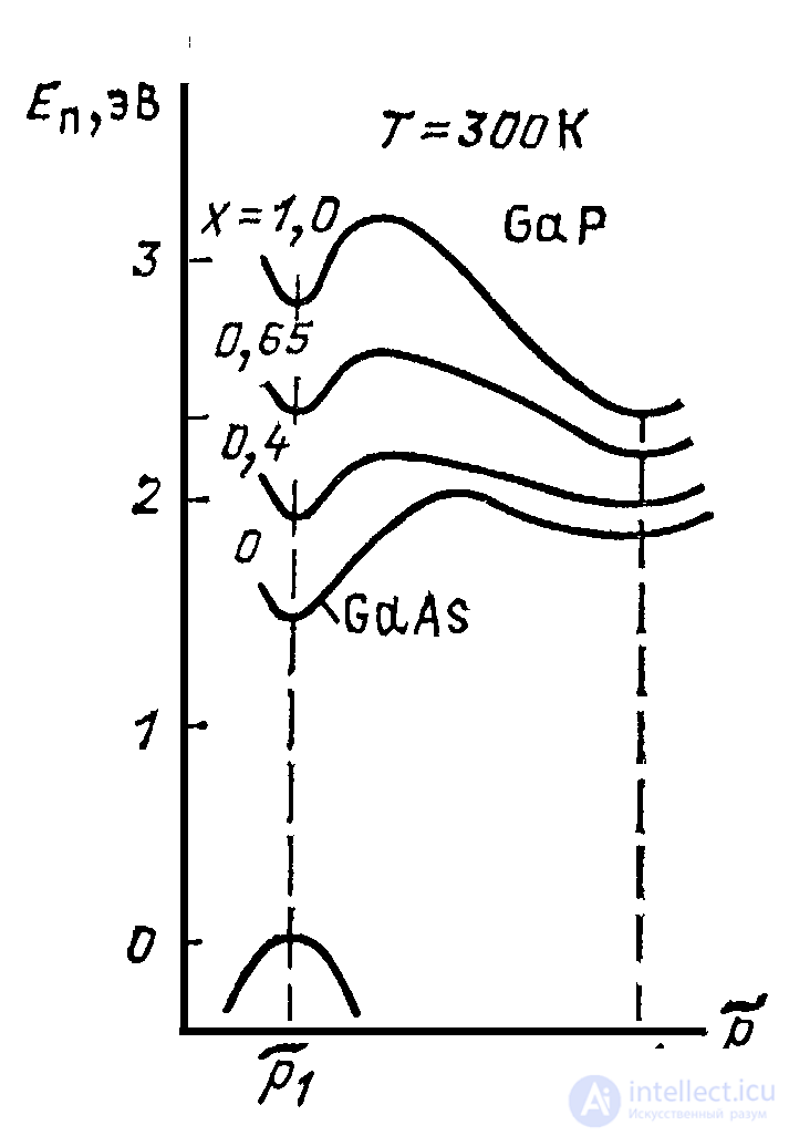
Fig.1
The main semiconductor materials used for LEDs are gallium arsenide (GaAs), gallium phosphide (GaP), gallium nitride (GaN), silicon carbide (SiC), the ternary solid solution of gallium phosphide and arsenide (GaAs1-xPx), where  , and a number of other binary and multicomponent semiconductor compounds. The use of these materials makes it possible to create LEDs operating in the infrared, visible and ultraviolet regions of the spectrum. The efficiency of the devices under consideration mainly depends on the internal quantum yield
  . The probability of radiative recombination, which determines the internal quantum yield, is directly related to the type of transitions in the semiconductor used. The internal quantum yield in semiconductors with direct transitions is many times greater than in those with indirect transitions.
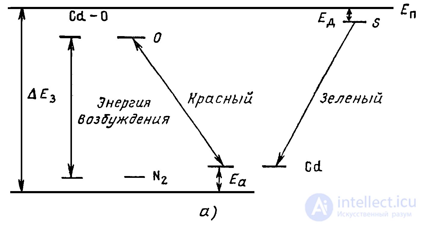 Fig.2
Fig.2
Gallium phosphide based LEDs. Fig.1 (curve x=1.0) shows the energy band diagram of gallium phosphide, where the energy minima of the conduction band bottom at momentum value 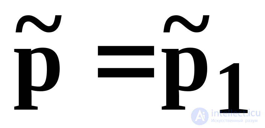 correspond to direct transitions (band gap width 2.8 eV), while at
 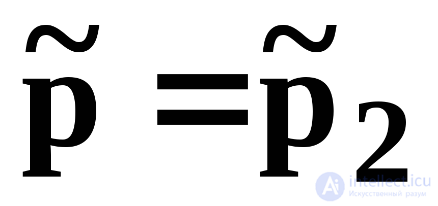 - to indirect transitions (
 =2.26 eV). Consequently, pure gallium phosphide GaP belongs to the indirect-band-gap semiconductors. Its quantum yield is insignificant, however it is widely used for manufacturing LEDs, since it provides emission in the visible region of the spectrum, which is especially important in indicator devices. To increase the efficiency of radiative processes in indirect-band-gap semiconductors, recombination centers - traps - are created by introducing impurities. When different elements are introduced, two types of traps are formed - donor and acceptor types. Radiative transitions between donor and acceptor traps make it possible to obtain light generation at various wavelengths (Fig.2, 3). When zinc, cadmium and oxygen are introduced, red emission is produced; cadmium, sulfur and nitrogen produce green emission (see Fig.2). The physical phenomena occurring in gallium phosphide in the presence of impurities can be illustrated using nitrogen doping as an example. Nitrogen replaces phosphorus atoms at the sites of the crystal lattice. Nitrogen and phosphorus are elements of the same group of the periodic table and have identical outer but different inner electronic structures. The difference in structure leads to the appearance of a trap energy level near the conduction b
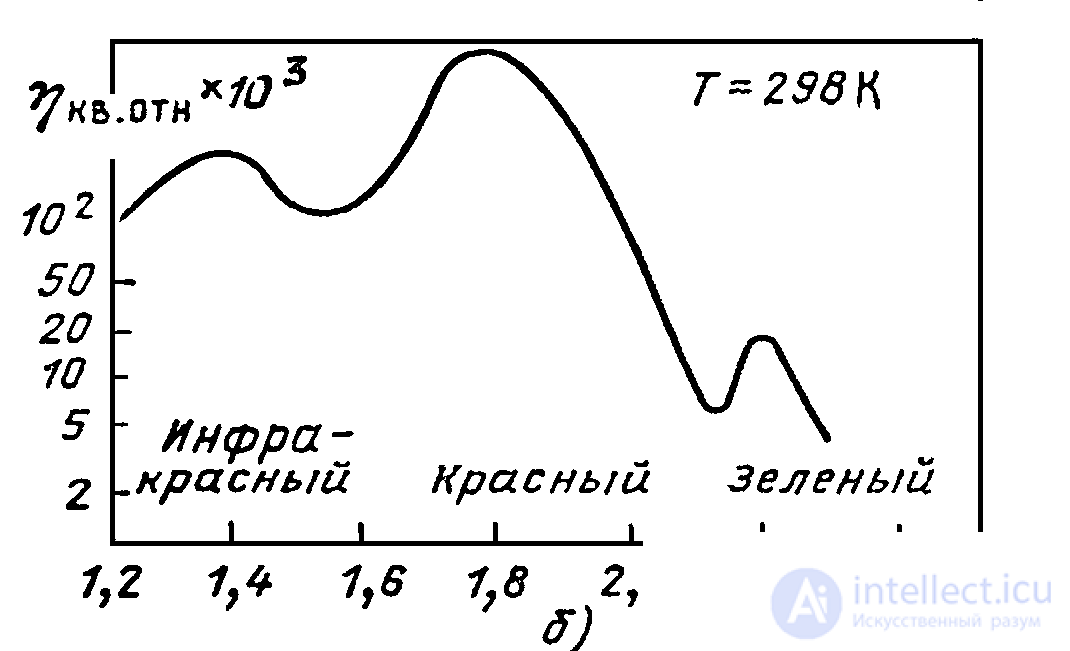 Fig.3
Fig.3
and. Electrons injected from the n- into the p-region of the LED first arrive at trap levels, which then capture a hole from the valence band. As a result, photons are generated with an energy approximately equal to the difference between the band-gap energy and the binding energy of the trap atom.
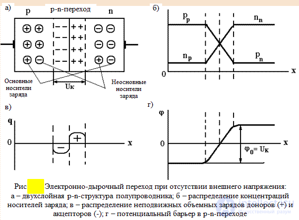
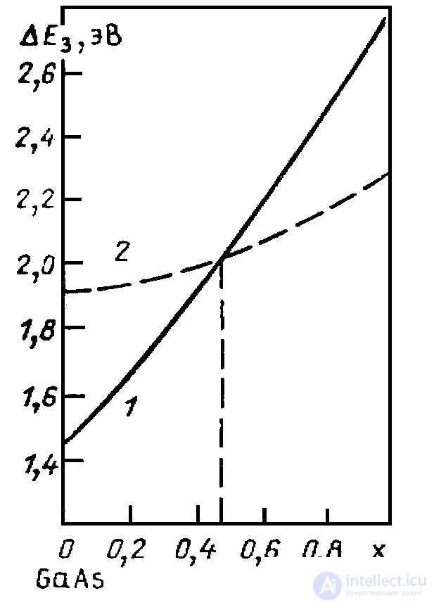 Fig.4
Fig.4
The dependence of the internal quantum yield  (in relative units) on the energy of the emitted photons is shown in Fig.3. The overall efficiency of an LED emitting green light is approximately equal to 0.1%, while for one emitting red light it is 3%. Although the efficiency of green-emitting LEDs is low, they are used in indicator technology, since the sensitivity of the eye to green light is 30 times higher than to red light.
Gallium arsenide based LEDs. As the phosphorus content in the gallium arsenide lattice increases, the energy band diagram of the semiconductor changes (see Fig.1). At x=0 the energy band diagram (curve 1) corresponds to pure gallium arsenide, and at x=1 to pure gallium phosphide. As x increases from 0 to 0.45, the band gap width of the compound  increases from 1.42 eV to 1.98 eV (Fig.4). In LEDs based on such materials, direct transitions predominate (curve 1 in Fig.4). A further increase in phosphorus content leads to indirect transitions (curve 2 in Fi
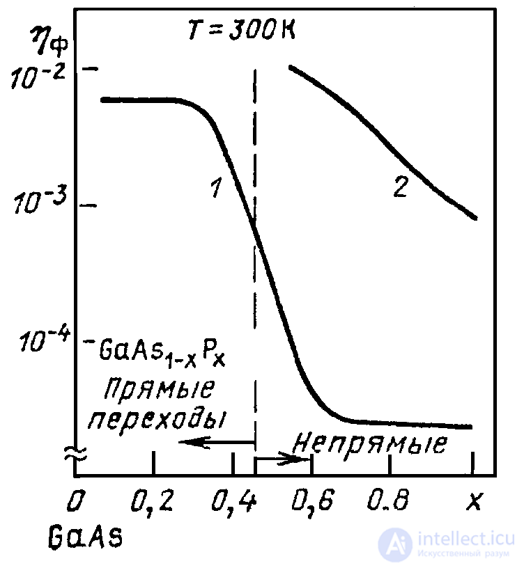 Fig.5
Fig.5
g.4), which causes a decrease in the probability of interband radiative recombination and, accordingly, of the internal quantum yield (curve 1 in Fig.5). To increase the efficiency of radiative recombination in gallium arsenide phosphide, as in gallium phosphide, impurities are introduced. Fig.5 illustrates the effect of nitrogen on the value of the external quantum efficiency ext, which represents the ratio of the number of photons emitted by the LED to the number of charge carriers flowing through its electrical junction.
The main parameters of LEDs include the following:
Brightness B (cd/m2) characterizes the glow of the LED in a selected direction. For LEDs, brightness amounts to several hundred cd/m2.
The minimum forward operating, or threshold, voltage Uth of the LED is determined by the energy of the emitted photons; for example, for green light the photon energy is 2.2 eV, while the threshold voltage is 2.4 eV.
The maximum operating voltage is limited by the allowable power dissipation of the LED. It mainly depends on the contact potential difference of the p-n junction and the resistance of the base. These voltages also determine the corresponding LED currents.
The rise time constant and the pulse decay time constant of the emission under pulsed excitation of LEDs characterize their inertial properties. These parameters are measured between brightness values equal to 0.1 and 0.9 of the maximum value. The inertia of LEDs is determined by the recharge time of the device's capacitance. For LEDs, the values of the time constants amount to fractions of a microsecond.
Efficiency depends on the internal quantum yield and the design of the LEDs. Energy losses are associated with light absorption in the semiconductor, contacts, and structural elements of the device.
And other well-known ones, such as: radiant power, the wavelength of the emitted light or its color, the maximum forward or pulsed current, longevity, etc.
These include:
-
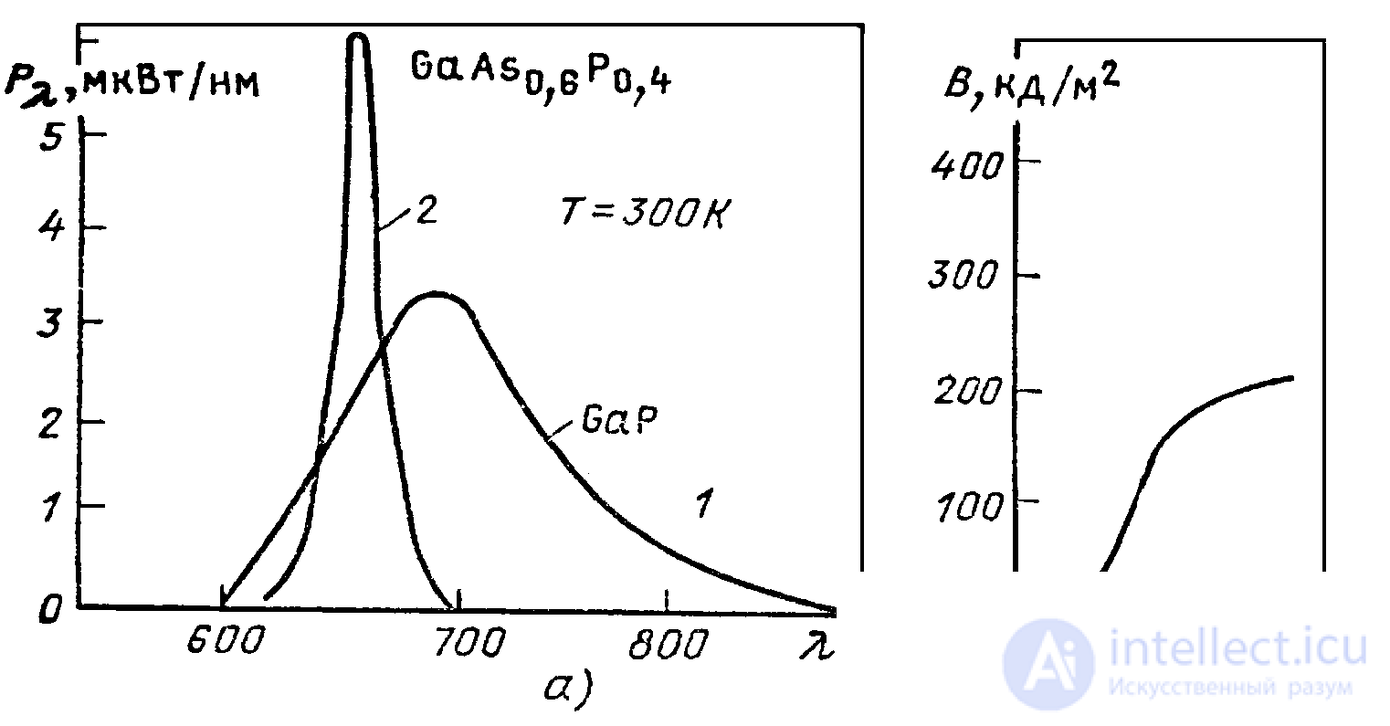 Fig. 6
Brightness characteristic - this is the dependence of brightness B on the current through the p-n junction. The shape of the brightness characteristic depends on the structure of the p-n junction and the region in which the predominant recombination of charge carriers occurs. At small currents and, correspondingly, small voltages, there is no emission. Emission arises at voltages corresponding to the energy of the emitted photon, approximately equal to the band-gap width, i.e., at U=Uthr (the voltage Uthr corresponds to Ithr on (Fig. 6b). An increase in voltage (current) increases the number of carriers recombining with emission, and the brightness increases. At high currents, non-radiative recombination due to trap filling begins to manifest strongly, as a result of which the quantum yield decreases and the slope of the characteristic to the abscissa axis becomes smaller.
- Spectral characteristic – this is the dependence of the intensity of the light flux (brightness, or power, or luminous intensity, or energy) on wavelength. (Fig. 6a) shows spectral characteristics giving the dependence of relative power on the emission wavelength, for an LED made of gallium phosphide (curve 1) and gallium arsenide phosphide (curve 2).
- Current-voltage characteristic I=(U) – coincides with the CVC of an ordinary diode.
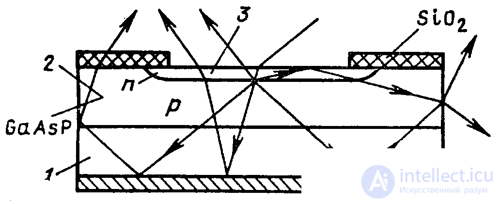 Fig. 7
The structural design of LEDs strongly affects the magnitude of the external quantum yield and, consequently, the efficiency of the device. Because of the high refractive index of the LED's base material, most of the light undergoes total internal reflection at the semiconductor-air interface. As a result, due to multiple re-reflections from the boundaries (Fig. 7), light is absorbed in the semiconductor, and only a small fraction of the radiated energy escapes from LEDs of the simplest flat design.
LEDs based on gallium arsenide phosphide (see Fig. 8) are produced by growing epitaxial layer 2 on a gallium arsenide substrate 1. Light emitted in the region of p-n junction 3 falls on substrate 1 and is partially absorbed, which leads to additional energy losses. With improved technology, epitaxial layer 2 is grown on a transparent gallium phosphide substrate with a reflective bottom coating. This increases the yield of useful radiation. The external quantum yield can also be increased through the use of more complex LED designs.
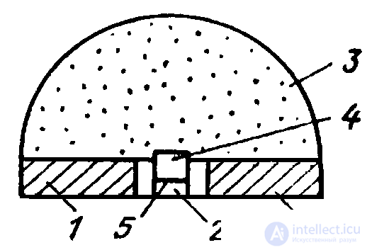 Fig. 8
Fig. 8 shows an example of the construction of such an LED, in which 3 is the n-base, made in the form of a hemispherical semiconductor single crystal, 1 and 2 are metal contacts, and 4 is the emitter. To increase the efficiency of LEDs, transparent hemispherical coatings of glass and plastics with a high refractive index are used, as well as anti-reflective (transparent to the emitted waves) coatings on the outer surface of the device, etc.
To obtain light of different colors in indicators or indicator matrices, LEDs can have several junctions. Ex
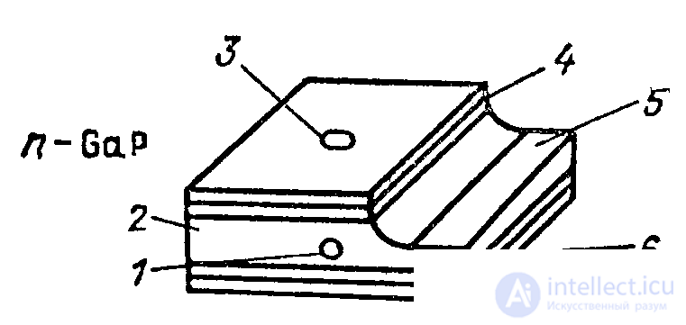 Fig. 9
ample of a double-diode structure that emits red or green light, or both at the same time, is shown in Fig. 9, where 1 and 3 are contacts to the p-regions of the diode generating red and green light respectively; 2 is the n- GaP substrate; and 4 and 6 are the p-n junctions; 5 is the common contact.
In practice, devices based on pure gallium arsenide emitting infrared light (=900 nm), gallium nitride - blue light, and other materials with characteristics inferior to those discussed are also used.
High reliability, long service life (durability), low operating voltages and power consumption, and the small mass and dimensions of LEDs have led to their widespread use in devices for a very wide range of purposes.
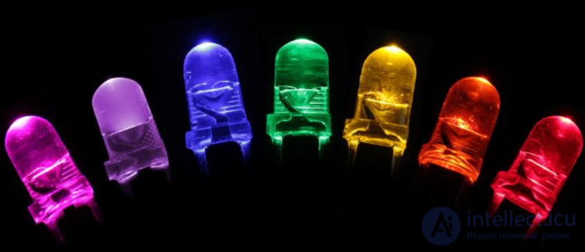
Ordinary LEDs are made of various inorganic semiconductor materials; the following table shows the available colors with their wavelength ranges, the voltage drop across the diode, and the material:
| Color | wavelength (nm) | Voltage (V) | Semiconductor material | |
|---|---|---|---|---|
| Infrared | λ > 760 | ΔU < 1.9 | Gallium arsenide (GaAs) Aluminium gallium arsenide (AlGaAs) |
|
| Red | 610 < λ < 760 | 1.63 < ΔU < 2.03 | Aluminium-gallium arsenide (AlGaAs) Gallium arsenide-phosphide (GaAsP) Aluminium-gallium-indium phosphide (AlGaInP) Gallium(III) phosphide (GaP) |
|
| Orange | 590 < λ < 610 | 2.03 < ΔU < 2.10 | Gallium phosphide-arsenide (GaAsP) Aluminium-gallium-indium phosphide (AlGaInP) Gallium(III) phosphide (GaP) |
|
| Yellow | 570 < λ < 590 | 2.10 < ΔU < 2.18 | Gallium arsenide phosphide (GaAsP) Aluminium gallium indium phosphide (AlGaInP) Gallium(III) phosphide (GaP) |
|
| Green | 500 < λ < 570 | 1.9[15] < ΔU < 4.0 | Indium gallium nitride (InGaN) / Gallium(III) nitride (GaN) Gallium(III) phosphide (GaP) Aluminium gallium indium phosphide (AlGaInP) Aluminium gallium phosphide (AlGaP) |
|
| Blue | 450 < λ < 500 | 2.48 < ΔU < 3.7 | Zinc selenide (ZnSe) Indium gallium nitride (InGaN) Silicon carbide (SiC) as substrate Silicon (Si) as substrate — (under development) |
|
| Violet | 400 < λ < 450 | 2.76 < ΔU < 4.0 | Indium gallium nitride (InGaN) | |
| Purple | Mixture of several spectra | 2.48 < ΔU < 3.7 | Dual: blue/red diode, blue with red phosphor, or white with purple plastic |
|
| Ultraviolet | λ < 400 | 3.1 < ΔU < 4.4 | Diamond (235 nm)[16]
Boron nitride (215 nm)[17][18] |
|
| White | Broad spectrum | ΔU ≈ 3.5 | Combination of three primary-color LEDs (red, blue, green), or a phosphor that emits white light under excitation from an LED with a spectrum ranging from blue to ultraviolet; |
Multilayer thin-film structures made of organic compounds that efficiently emit light when an electric current is passed through them. OLEDs are mainly used in the creation of information display devices (displays). It is expected that the production of such displays will be much cheaper than that of liquid-crystal displays.
The main problem for OLEDs is continuous operating time, which must be no less than 15 thousand hours. One of the problems currently hindering the widespread adoption of this technology is that «red» OLEDs and «green» OLEDs can operate continuously for tens of thousands of hours longer than «blue» OLEDs. This visually distorts the image, and the time of quality display is unacceptable for a commercially viable device. Although today «blue» OLEDs have nevertheless reached the mark of 17.5 thousand hours (2 years) of continuous operation.
Displays made of organic light-emitting diodes are used in the latest models of mobile phones, GPS navigators, OLED televisions, and for creating night-vision devices.
Compared to other electric light sources, LEDs have the following distinguishing features:
high cost

Comments