
Lecture
A solar converter, or solar photocell, is a semiconductor device that converts optical solar radiation into electrical energy.
A collection of solar converters combined into a single, usually flat, panel-type structure is called a solar battery. Solar batteries are the main source of energy on satellites and space power installations of various capacities.
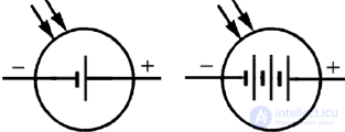
Symbol for solar batteries in electrical diagrams
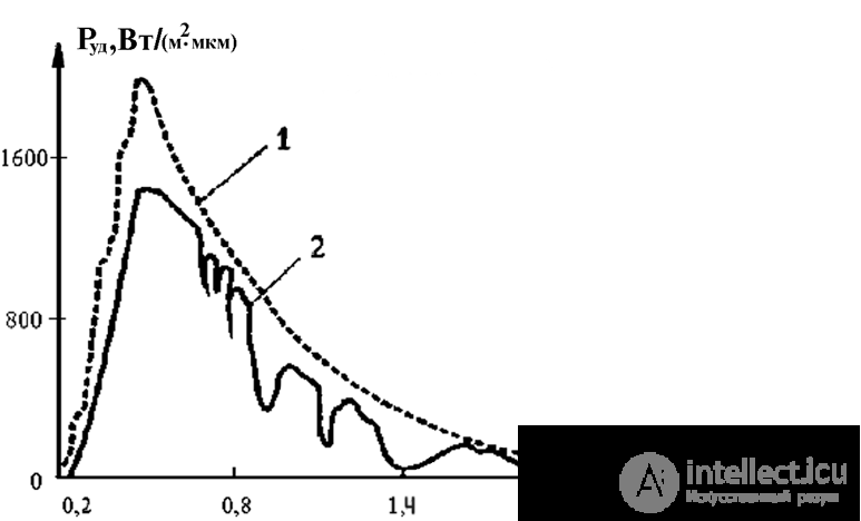 Fig.1
Fig.1
Since solar converters (SC) are intended to convert solar energy, one must strive to ideally match their spectral characteristics with the spectrum of solar radiation. Fig.1 shows the distribution of solar energy over the spectrum: curve 1 corresponds to the solar spectrum in free space beyond the atmosphere, i.e. under the conditions in which SCs operate on satellites and spacecraft; curve 2 - the solar spectrum at the Earth's surface when the Sun is at its zenith. For the first case (curve 1) the total radiation power is 1353 W/m2, for the second - 925 W/m2.
Let us consider the basic physical processes occurring in a solar converter.
At
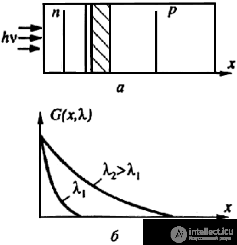 Fig.2
Fig.2
the basis of the design of an ordinary solar cell lies an illuminated p-n junction operating without external electrical bias. Solar cells make use of intrinsic absorption, whereby the energy required to ionize one atom is hv=Eg. The remaining photon energy is converted into heat. The generation rate decreases with distance from the surface, with short wavelengths being absorbed in higher layers compared to longer ones. The generation rate of electron-hole pairs as a function of distance from the solar cell surface (Fig.2.a) for long-wavelength and short-wavelength radiation is shown in Fig.2.b, where the shaded area corresponds to the p-n junction. Since a large number of photocarriers are generated in the upper layers, they begin, by diffusion, to move toward the depleted region of the junction, where they are separated by the junction's internal field. Electrons remain in the n-region, while holes, for which the junction field is accelerating, are swept into the p-region. Electrons and holes generated in the depletion layer under the action of light are carried out of it by the strong electric field of the junction, with practically no recombination. Therefore the photocurrent of the depletion layer is determined by the number of photons absorbed in that layer per unit time.
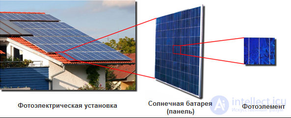
External view of a solar battery
The total photocurrent arising in a photocell upon light absorption equals the sum of the hole and electron currents flowing across the junction boundaries, plus the drift photocurrent generated directly in the p-n junction.
If the cell's circuit is open, photocarriers accumulate in the corresponding regions and compensate part of the space charge of impurity ions in the depleted region of the p-n junction. The potential barrier at the junction decreases in proportion to the degree of compensation of this charge, and an open-circuit voltage Uoc. appears at the cell's terminals. This phenomenon is called the photovoltaic effect (see the lecture «Photodiodes»).
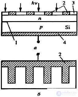 Fig.3
Fig.3
If the circuit is short-circuited (RL=0), a short-circuit current Isc will flow through it, caused by photocarriers. In the presence of a load, i.e. when RL is not equal to 0, a current smaller than Isc flows in the circuit, and across RL a voltage drop UL. develops. If an external reverse bias is applied to the illuminated element, the reverse current of the p-n junction is added to the photocurrent, i.e. under reverse bias the total current equals Isc+Irev. At forward biases greater than Uoc, the injection current through the junction begins to dominate over the photocurrent, and the illuminated junction behaves as an ordinary p-n junction.
There exist quite a variety of solar cell designs. As an example, let us consider the structure of a silicon solar cell (Fig.3), since these devices serve as a kind of standard in the fabrication of all solar batteries.
The solar cell shown in Fig.3.a,b consists of a p-n junction 1 formed near the surface; a front (surface) strip-type ohmic contact 2; an antireflection coating on the front surface 3; and a continuous rear ohmic contact 4. Fig.3.b illustrates the structure of the strip electrode 2 as seen from above. The drawback of this design is the shadow cast by the metal contacts, which reduces the device's efficiency, and a high reflection coefficient of light from the element's surface.
One of the best-performing designs is the solar cell shown in Fig.4, where 1 is a textured surface with an increased level of donor doping - n+; 2 is the p-region of the cell; 3 - the metal contacts of the n+ collector; 4 - the metal leads of the base. On top the cell has an antireflection coating (not shown in the figure). In the cell under consideration there is no shadowing from metal electrodes, and interconnecting the cells is simpler to implement, since here the electrodes are located on the rear surface. This device functions similarly to a bipolar transistor n+-p-n+ type with an isolated n+ emitter located on the textured front surface.
N
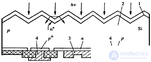 Fig.4
Fig.4
on-equilibrium electron-hole pairs, generated by light in the n+ emitter (1) or the p - base (2), move (like in an ordinary transistor) toward the n+ collector and are separated by the collector junction. Electrons enter the n+ collector, while holes remain in the p - base, whose leads (4) are made through the p+ regions. In this photocell, near the back (lower in Fig.4) surface, in front of the metal ohmic contacts, heavily doped semiconductor layers p are created. Between the two base regions p+ and p a potential barrier arises that prevents electrons from leaving the p - region.
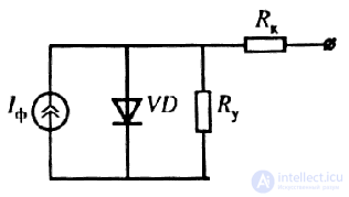 Fig.5
Fig.5
As a result, the surface recombination velocity of Si electrons near the back surface sharply decreases, i.e. photocarrier losses are reduced. The short-circuit current density increases, and the open-circuit voltage also rises due to the growth of Isc, the reduction of the recombination current of the back contact, and the additional potential barrier between the p+ and p- regions. Thus, the presence of a textured surface, which reduces reflection losses, and heavily doped regions on the back surface make it possible to achieve an efficiency of 20% or more.
To analyze the electrical circuit into which the photocell is connected, its equivalent circuit is used, which is shown in Fig.5. The current generator Iph determines the generation of non-equilibrium carriers due to illumination by light, diode VD models an idealized p-n junction, whose I-V characteristic is descri
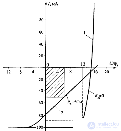 Fig.6
Fig.6
bed on Fig.6 (curve 1); the parallel resistance Rsh is due to leakage currents (in reality Rsh has a large resistance, so its effect on the output power can be neglected); the series resistance Rs is determined mainly by the resistance of the high-resistivity base region. Rs of the solar cell depends on the depth of the junction, the impurity concentration in the n- and p- regions, and the design of the front ohmic contact (see Fig.3). Its effect is very significant, even at values less than one ohm. Thus at Rs=5 Ohm the output power decreases by more than 30% compared to the power at Rs=0.
Fig.6 illustrates the effect of Rs on the I-V characteristic; it also shows a shaded rectangle whose area determines the maximum power produced by the photocell at Rs=5 Ohm (P = 0.27 W), and an unshaded rectangle for the power at Rs=0 (P = 1 W).
In real solar cells, unlike ideal ones, the forward current may be determined by carrier recombination in the p-n junction, which reduces the conversion efficiency. In silicon solar cells at room temperature, the recombination current leads to a decrease in conversion efficiency of 25%.
An increase in temperature also reduces the conversion efficiency (η), mainly due to a decrease in Uoc caused by an increase in the reverse saturation current Irev at high temperatures.
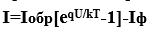
The I-V characteristic of solar cells with p – n junctions is determined by the expression:
 (1)
(1)
where Irev - the reverse current of an ideal p-n junction; Iph- photocurrent.
Heterojunctions are junctions that form at the contact between two semiconductors with different band gaps. If the top layer of the photocell, on which the light falls, is made of a semiconductor with a wide band gap  , and the bottom layer with a narrow one
  , then upon irradiation with photons of energy
 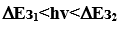 they pass through the layer of the first semiconductor and are absorbed in the second. The first layer with a wide band gap
  plays the role of an optical window.
The main advantages of solar cells with heterojunctions: 1) the spectral response at short wavelengths improves, provided that  and the photons are absorbed in the depletion layer of the second semiconductor; 2) it becomes possible to obtain a low series resistance due to heavy doping of the top layer; 3) high radiation resistance when the top semiconductor layer is sufficiently thick and wide-gap.
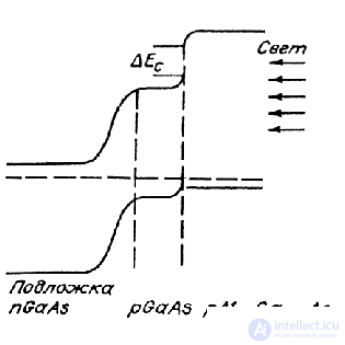 Fig.7
Fig.7
The band energy diagram of solar cells (SC) is shown in Fig.7, where the pAlxGa1-xAs layer is fairly thick (20...30 μm) (the indices x and 1-x show the fractional mass composition of each component, where x – lies in the range from 0 to 1). To obtain the specified SC structure, nGaAs was used as the substrate. The thickness of the pGaAs diffusion region was usually within 1...3 μm. The carrier concentration in pAlxGa1-xAs was (1..5)-1018 cm-3.
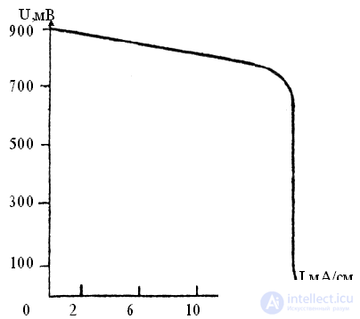 Fig.8
Fig.8
A typical load characteristic, measured at a light flux power of 1375 W/m, is shown in Fig.8. On samples with an area of 2...3 cm2, the following SC parameters were obtained: Uoc=0.87...0.95 V, Isc=15...20 mA/cm2 and efficiency=10...11%.
Such SCs with a thick wide-gap "window" have minimal series resistance. They can operate under concentrated solar radiation up to 1000 solar constants. Further improvement of the technology for manufacturing SCs with a thick "window", the use of anti-reflection coatings and an optimized contact grid led to an increase in efficiency up to 21.6%.
Thin-film solar cells are made from polycrystalline or disordered semiconductor films deposited or grown on electrically active or passive substrates (ceramic, metal, glass, plastic, silicon, etc.). They are widely used due to their low cost, resulting from the simplicity of the technology and the low cost of the materials used. However, these devices have low efficiency and degradation of characteristics over time, due to the fact that it is not yet possible to manufacture high-quality films that react weakly with the environment.
Recently, amorphous silicon, called a-Si, has been used as one of the main materials for manufacturing thin-film solar cells. Crystalline and amorphous silicon differ greatly. Unlike crystalline silicon, amorphous silicon is close in its properties to a direct-gap semiconductor with a bandgap width of 1.6 eV. SCs based on AlGaAs-GaAs heterojunctions are the most efficient of all currently known. However, their mass use is delayed by the high cost, which is largely determined by the cost of the monocrystalline GaAs substrate.
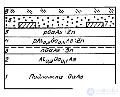 Fig.9
Fig.9
The physical processes that determine SC operation (generation and separation of electron-hole pairs by the contact field of the junction) usually occur at a depth of the order of several micrometers, so the substrate mainly serves as a carrier and provides mechanical strength at various stages of device manufacturing. The simplest way to reduce the cost of SCs based on AlGaAs-GaAs heterojunctions is to reduce the consumption of GaAs wafers as substrate material. This can be achieved by separating the finished structure from the substrate and reusing the substrate many times to grow TFSCs.
A schematic representation of the TFSC structure not separated from the substrate is shown in Fig.9.
Here layer 2 serves to separate the TFSC structure from the substrate by etching it in hydrofluoric or hydrochloric acid (i.e., the same substrate can be used many times to grow TFSCs).
During the growth of layer 4, a working p-n junction is formed in nGaAs due to zinc diffusion (dashed line in Fig.9). Layer 6 is necessary to ensure the ohmicity of the contact to pAl0,6Ga0,4As. The finished epitaxial structure (3, 4, 5) with contacts to the p-region 7 is glued to glass 8 using epoxy resin (layer 6).
Parameters of TFSC.
-
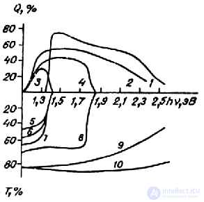 Fig.10
Spectral distribution of photosensitivity (Q, %) is shown in Fig.10: for 1 – TFSC AlGaAs/GaAs; 2 – Si photocell; 3 – Si photocell coated with TFSC AlGaAs/GaAs; 4 – Si photocell coated with a layer of Al0,25Ga0,76As (d=10μm);
- Transmission spectra of structures (T, %) 5-7 – glass - epoxy resin – TFSC AlGaAs/GaAs; 8 – glass – epoxy resin – layer Al0,25- Ga0,76As; 9, 10 – glass – epoxy resin – glass without heat treatment (7,10) and after heat treatment at temperature; 6 – at a temperature of 250 C; 9 - at a temperature of 320 C.
The ideal conversion efficiency ( ) of optical radiation into electrical energy is achieved with such a choice and fabrication of the material that the reverse current is minimal; efficiency is determined by the ratio of the maximum output power to the power of the incident radiation. The limiting values of the ideal efficiency can be obtained if it is assumed that the losses in the photocell are due only to radiative recombination.
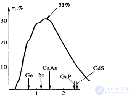 Fig.11
It would seem that to obtain maximum efficiency it is necessary to have minimal values ofIrev and, consequently, it is advisable to use semiconductors with as wide a bandgap as possible. However, between the bandgap width and the photon energy there exist optimal ratios for each real crystal. If  , then the energy difference hv-Eg is mainly converted into heat. Moreover, as can be seen from Fig.1, in the solar radiation spectrum most of the photon flux has an energy on the order of one electron-volt. Taking this into account, on the basis of the calculations performed it was shown that the maximum efficiency is achieved at
 =1.35 eV. Fig.11 shows the dependence of the efficiency
  for a solar cell located on Earth at T=300 K and illuminated by the Sun at an angle of 45 to the horizon. If a thousand-fold concentration of sunlight is achieved, the maximum efficiency increases from 31% to 37%, which is related to the increase in Uoc. The arrows in the figure indicate the bandgap width values for some semiconductors – germanium Ge, silicon Si, gallium arsenide GaAs, and others. In real solar converters the maximum efficiency is noticeably lower than the ideal one due to the influence of the resistance of the high-resistivity base region, various types of recombination, resistive losses, and a number of other factors. The quantum efficiency has the decisive influence on the efficiency of the devices under consideration.
Silicon and gallium arsenide are used in p-n junction converters, but preference is given to silicon. This is due to the fact that the manufacturing technology of silicon SC is well established, and their parameters are stable over a temperature range (-150…+150C). A film of silicon monoxide forms an anti-reflective coating on the surface of the crystal and reduces the reflection coefficient. The diffusion length of minority carriers in silicon is greater than in gallium arsenide, so the efficiency and Isc of a silicon converter are higher.
A radical way to increase the efficiency of SC is to create cascade (tandem) cells.
The design of a cascade solar cell is a series connection of SCs made on the basis of different semiconductor materials. The latter are arranged in order of decreasing bandgap width so that the top cell, converting short-wavelength radiation, passes the longer-wavelength radiation through itself, which is then converted by the cell below it. The generated EMFs of the cells are summed, and the total current is determined by the minimum current of any cell in the cascade. For the CSC to operate efficiently, current matching of each cell is required. Theoretical analysis of the maximum possible efficiency, with two cells connected in series, gave 50%. A further increase in the number of junctions leads to only a small increase in efficiency, and at 36 junctions the maximum efficiency equals 72%.
Let us consider some experimental results obtained in the development of CSCs. Fig.12 shows two designs often used when creating CSCs, based on a monolithic structure (a) and a transistor structure (b), where:
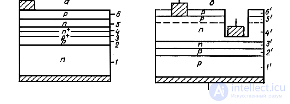 Fig. 12
1 – nGaAs substrate; 2 – pGaAs:Ge layer; 3,4,5 – Al0.2Ga0.8As layers; 6 – Al0.9Ga0.1As layer; 1`– pGaAs substrate; 2`– pGaAs:Ge buffer layer; 3`– nGaAs; 4`– nAl0.2Ga0.8As; 5`– pAl0.2Ga0.8As; 6`– pAl0.9Ga0.1As
The monolithic CSC structure (Fig.12.a) is an nGaAs substrate, on the surface of which layers 2 - 6 are grown in sequence. Layer 2 and the substrate form the narrow-bandgap cell of the cascade. Layers 5 and 6 form the wide-bandgap cell of the cascade, and the connecting element is a tunnel diode formed by layers 3 and 4. The efficiency values obtained by this method are in the range of 15 - 20%.
The transistor CSC structure (Fig.12.b) is a pGaAs substrate, on the surface of which a pGaAs buffer layer (2) and an epitaxial nGaAs layer (3) are grown. The wide-bandgap cell of the cascade is formed by layers 4 and 5, where the p-n junction is formed in the Al0.2Ga0.8As solid solution. Layer 5 is formed by diffusion during the growth of layer 6. In such CSC designs the efficiency reaches 20.5% and 26% for 10-fold concentration of solar radiation.
The widespread use of SC in the national economy is being delayed due to the high cost. To reduce the cost of solar cells, a search is currently underway worldwide for cheap materials, as well as new technologies and design solutions. It is known that monocrystalline silicon SCs currently have an efficiency of ~18%, while the theoretical efficiency limit is 22%.
The first reports on reducing the cost of SC relate to the creation of thin-film SCs based on homojunctions (n+-p-p+) in polycrystalline gallium arsenide deposited on graphite-coated tungsten substrates and on aluminum substrates. On an SC with an area of ~1 cm the efficiency is 8.1%. When creating SCs on aluminum substrates using Ga as a solvent, an efficiency of about 14% can be obtained.
To preserve the high efficiency of GaAs-based SCs while simultaneously reducing their cost, research is underway on the growth of monocrystalline GaAs layers on silicon substrates with a germanium sublayer. This makes it possible to reduce the mass of the SC, since Si has a density 0.44 times lower than GaAs, which appears important for the creation of solar arrays for space applications.

Comments