
Lecture
X-ray lithography — a technology for manufacturing electronic microcircuits; a variant of photolithography that uses exposure (irradiation) of a resist by means of X-rays.
X-ray lithography uses soft X-radiation with a wavelength of 0.4-5.0 nm. A beam of X-rays is passed through a mask and exposes a layer of resist. The optical elements of X-ray lithography systems can be reflecting mirrors (reflectors) based on nanoheterostructures with Ni-C, Cr-C, Co-C, Mo-C, W-C layers, and zone plates; thin (1 µm or less) metal membranes are used as masks. Multilayer X-ray mirrors provide Bragg reflection under the condition d = λ/(2sinΘ), where d is the period of the structure and Θ is the grazing angle. At normal incidence of the radiation Θ = 90° and the period d = λ/2, so the thickness of each layer in an X-ray mirror is approximately λ/4, or 1 nm.
X-ray lithography, like optical lithography, is carried out by simultaneously exposing a large number of pattern details, but short-wavelength X-radiation makes it possible to create a pattern with finer details and higher resolution.
Owing to the short wavelength of X-radiation, X-ray lithography methods possess a high resolving power (~ 10 nm). Compared with electron-beam and ion-beam lithography, X-ray lithography causes little radiation damage to the structures being formed and offers high throughput thanks to the possibility of simultaneously processing large areas of the sample. X-ray lithography is distinguished by a large depth of focus and a weak influence of the substrate material and its topography on resolving power.
Like electron-beam lithography, X-ray lithography eliminates the diffraction limitations of the radiation. Exposure uses "soft" X-rays with a wavelength of 0.4 - 50 nm, excited by means of intense electron beams. Scattering of X-ray quanta in the substrate is much smaller than the scattering of electrons, which limits the achievable resolving power of electron-beam lithography. Such advantages as high resolving power (less than 0.01 µm), a large depth of focus (up to tens of micrometers), which provides for exposure with a large gap and, consequently, mask durability, low sensitivity to dust particles and other contaminants, and insensitivity to external magnetic and electric fields, make X-ray lithography one of the most reliable methods for creating high-density ICs.
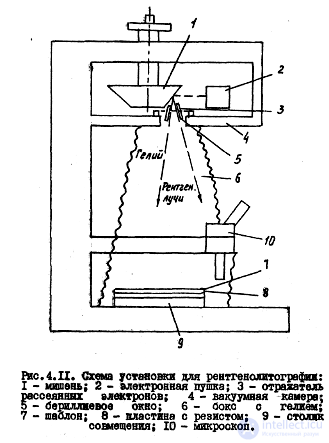
Fig. 4.11 shows the layout of an X-ray lithography system.
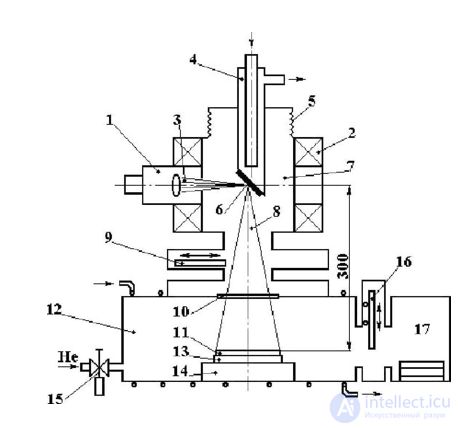
1 - electron gun:
2 - magnetic focusing system:
3 - electron beam:
4 - cooled anode;
5 - alignment device;
6 - fixed anode - emitter;
7 - source chamber;
8 - X-ray beam;
9 - shutter;
10 - exit window;
11 - X-ray mask;
12 - exposure chamber;
13 - substrate;
14 - carrier;
15 - leak valve;
16 - gate valve:
17 - load-lock chamber.
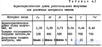
X-radiation is obtained by exposing a target to a focused electron beam. Various metals are used as the target (Table 4.1).
The electron beam, directed by the electron gun, is focused on the target. In order to provide a sufficiently powerful flux of X-radiation, the target must be cooled with water and rotated at high speed (otherwise it would melt); this assembly is the 'weak point' of X-ray lithography systems. Typical systems have a target diameter of about 10 cm, an electron-beam power of 10 - 25 kW, a beam diameter of a few millimeters, and a target-to-resist distance ranging from 15 to 50 cm. The X-ray beam passes through a scattered-electron reflector and is extracted from the vacuum chamber through a thin beryllium window. Inside a helium-filled enclosure (the attenuation of X-radiation in helium is much greater than in air) are the mask and the resist-coated wafer, mounted on an alignment stage. Alignment is performed by several methods, the simplest of which is optical, using a high-magnification microscope.
The theoretical resolution limit of X-ray lithography is less than 0.1 µm. In practice this has not yet been achieved. This is due, first, to the appearance of photoelectrons generated by the X-radiation, which cause a broadening
of the line by about 100 nm, and, second, to two forms of distortion that arise during exposure.
Let us note the causes of these distortions:
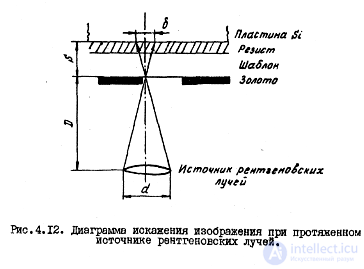
I. If the X-ray source is extended, a penumbral distortion arises. Fig. 4.12 shows the distortion diagram for this case. The distortion can be determined by the formula:
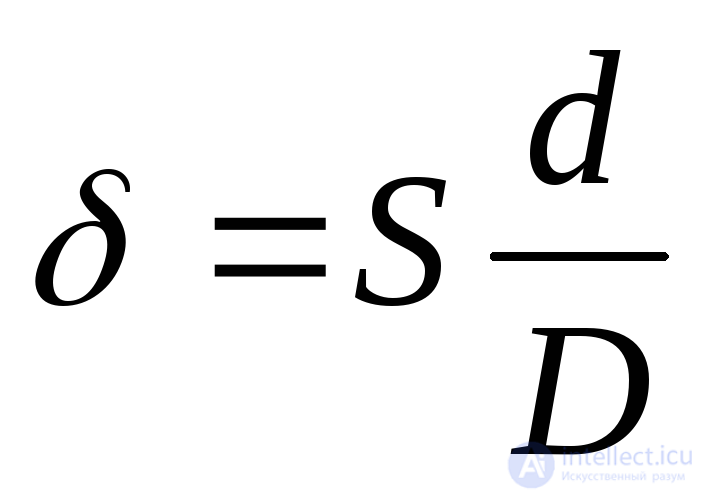 (4.9)
(4.9)
where S is the gap between the mask and the wafer; d is the length of the radiation source; D is the distance between the radiation source and the mask.
Because of the low mechanical strength of the X-ray mask, a gap between the wafer and the mask is a necessary measure.
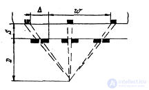
Fig. 4.13. Diagram of image distortion for a point source of X-rays.
Submicron printing is provided with a mask-to-wafer gap on the order of 1 µm. Warping of the wafer, which arises during many standard process steps, makes such a gap difficult to achieve.
Errors associated with the gap can be partly eliminated by switching to step-and-repeat exposure or by increasing the resist sensitivity to 1 mJ/cm2, which would allow the radiation source to be moved farther from the wafer. The main difficulties are related to the thermal stability of the mask, since heating of the mask by the exposing radiation leads to changes in the in-plane dimensions of elements and to alignment errors.
Because of the low absorption, the X-ray exposure time is extremely long. The first steps toward improving X-ray printing (with a gap) are the development of:
1) highly sensitive resists;
2) an intense source;
3) a precise and reliable alignment system;
4) a transparent and stable mask.
2. With a point source, geometric distortion arises (Fig. 4.13). The magnitude of the geometric distortion is determined by the formula:
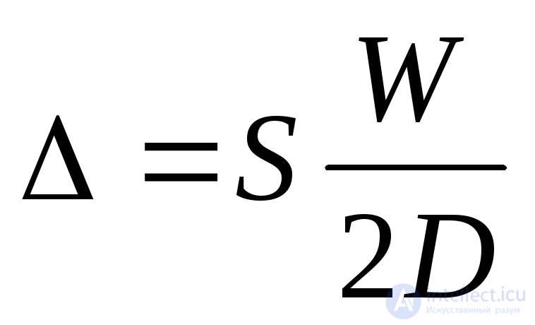 (4.10)
where W is the width (diameter) of the semiconductor wafer. This distortion can be accounted for when designing the mask if all the parameters entering formula (4.10) are kept constant. The most difficult parameter to keep constant is the gap between the mask and the wafer.
The choice of the X-radiation wavelength and of the mask substance through which the X-ray resist is exposed are interrelated.
The choice of target material, and consequently of the X-radiation wavelength, is made taking into account that photoresists are very sensitive to low-energy X-rays (long wavelength), but such radiation is strongly absorbed by the mask material. Hard X-radiation is not efficiently absorbed by the photoresist (less than 5%) and, moreover, requires thicker layers of absorbing mask coating (see Table 4.1), which in turn reduces the ability to obtain small images.
Creating the X-ray mask is a serious problem for this lithography method. The absorbing film must have sharp edges, be thin, and strongly attenuate the X-radiation. Thin films of gold, platinum, rhenium, and europium are used for this purpose. The mask substrate (membrane) must be mechanically strong and transmit as large a fraction of the incident radiation as possible. Films of various inorganic materials are used as the membrane, including  , as well as the polymers Mylar and polyimide. The thickness of the membrane depends on the wavelength of the radiation and is usually a few micrometers. When sources with a wavelength of less than 1.33 nm are used, the membrane absorbs the radiation intensively, and therefore its thickness must be reduced to 1 µm (see Table 4.1).
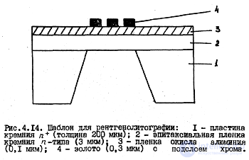
A silicon mask (Fig. 4.14) is a wafer with thinned window membranes. The membrane and the substrate on which it is formed are made of the same material and therefore have the same coefficient of thermal expansion. Fabrication begins with epitaxial growth of a lightly doped n-type layer on a heavily doped n+ substrate, onto which a thin layer of Al2O3 is deposited. An absorbing mask is created on the surface of this layer by electron-beam lithography. Then comes the most critical operation - slow etching of windows in the n+ silicon substrate (window area about 1 cm2).
Masks made of thin polymer film stretched over a support ring of steel or aluminum have a certain advantage over silicon masks.
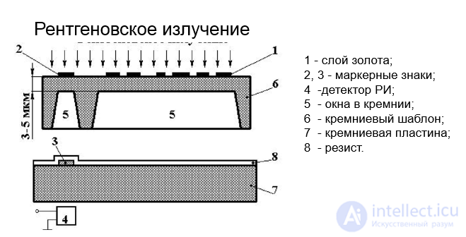
One of the serious problems in X-ray lithography is deformation of the mask during fabrication and use. The causes of deformation can be mechanical stresses in the membrane or different thermal expansion coefficients of the membrane and the mask frame.
To eliminate the drawbacks associated with distortion and the long exposure time in the X-ray lithography process, it has been proposed to use synchrotron radiation. It is generated by relativistic electrons as they move along curved trajectories in magnetic fields. Tangent to the trajectory of electrons accelerated to 1 GeV, a powerful plane-parallel beam of broad-spectrum X-radiation can be obtained. This method has produced lines 0.05 µm wide. The drawback of the process is the use of expensive equipment and the complexity of its operation.
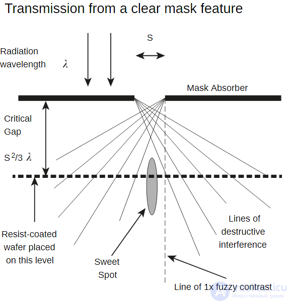
X-ray lithography originated as a candidate for next-generation lithography for the semiconductor industry , and batches of microprocessors were successfully produced. With short wavelengths (less than 1 nm), X-rays overcome the diffraction limits of optical lithography, providing smaller feature sizes. If the X-ray source is not collimated, as in the case of synchrotron radiation, then elementary collimating mirrors or diffractive lenses are used instead of refractive lenses, the kind used in optics. X-rays illuminate a mask placed close to the resist-coated wafer. The X-radiation is broadband, typically from a compact synchrotron radiation source, which provides rapid exposure. Deep X-ray lithography (DXRL) uses even shorter wavelengths, on the order of 0.1 nm, and modified procedures, such as the LIGA process, to create deep and even three-dimensional structures.
The mask consists of an X-ray absorber, usually gold or compounds of tantalum or tungsten, on a membrane transparent to X-rays, usually silicon carbide or diamond. The pattern on the mask is applied by direct-write electron-beam lithography onto a resist, which is created using conventional semiconductor processes. The membrane can be stretched for overlay accuracy.
Most demonstrations of X-ray lithography have been carried out by exact-scale (non-magnifying) copying along a line of soft contrast, as shown in the figure. However, with the growing need for high resolution, X-ray lithography is now performed in the so-called "sweet spot," using local "offset reduction." Dense structures are created by multiple exposure with translation. The advantages of using 3x reduction include easier mask fabrication, an increased gap between the mask and the wafer, and higher contrast. The technology is being extended to dense 15 nm prints.
X-rays generate secondary electrons, as in extreme ultraviolet lithography and electron-beam lithography. While sharp definition of the structure is mainly due to secondary particles from short-range Auger electrons, primary electrons will sensitize the resist over a larger area than the X-ray exposure itself. Although this does not affect the pattern-pitch resolution, which is determined by the wavelength and the gap, the exposure image contrast (max-min) / (max + min) decreases, because the pitch is on the order of the primary photoelectron range. These secondary electrons affect sidewall roughness and slope, since they can travel several micrometers in the region under the absorber, depending on the energy of the X-radiation. Several prints roughly 30 nm thick have been published.
Another manifestation of the photoelectric effect is the action of X-rays on electrons from the thick gold films used to fabricate daughter masks. Modeling shows that photoelectron generation at the gold substrate can affect the dissolution rate.
Secondary electrons have an energy of 25 eV or less and can be generated by any ionizing radiation (VUV, EUV, X-rays, ions, and other electrons). Auger electrons have energies of hundreds of electronvolts. Secondary electrons (generated by Auger and primary photoelectrons and outnumbering them) are the primary agents responsible for exposing the resist.
The relative ranges of primary photoelectrons and Auger electrons depend on their respective energies. These energies depend on the energy of the incident radiation and on the composition of the resist. There are many possibilities for optimal selection (reference 3 of the article). When Auger electrons have lower energy than primary photoelectrons, they have a shorter range. Both decay into secondary electrons, which interact with chemical bonds. When the secondary energies are too low, they cannot break chemical bonds and stop affecting print resolution. Experiments show that the combined range is less than 20 nm. On the other hand, secondary electrons show the opposite trend below ≈30 eV: the lower the energy, the longer the mean free path, although at that point they can no longer affect resist development.
As they decay, primary photoelectrons and Auger electrons eventually become physically indistinguishable (as in Fermi–Dirac statistics) from secondary electrons. The range of low-energy secondary electrons is sometimes greater than the range of primary photoelectrons or Auger electrons. What matters for X-ray lithography is the effective range of electrons that have enough energy to form or break chemical bonds in negative or positive resists.
X-rays do not carry a charge. The relatively long mean free path (~ 20 nm) of secondary electrons makes it difficult to control resolution at the nanometer scale. In particular, electron-beam lithography suffers from negative charging by the incident electrons and, as a result, beam blooming, which limits resolution. It is therefore difficult to isolate the effective range of secondary electrons, which may be less than 1 nm.
The combined electron mean free path causes image blur, which is typically modeled as a Gaussian function (where σ = the blur), convolved with the expected image. When the desired resolution approaches the blur, the dose image becomes wider than the aerial image of the incident X-rays. The blur that matters is the latent image, which describes the formation or breaking of bonds during resist exposure. The developed image is the final relief image obtained by applying the chosen high-contrast development process to the latent image.
According to various cited publications, the range of primary, Auger, secondary, and higher-order-generation ultra-low-energy electrons that contribute to printing (as STM studies have shown) can be large (tens of nm) or small (nm). Because this range is not a fixed number, it is difficult to quantify. Line-edge roughness is aggravated by the associated uncertainty. Line-edge roughness is presumed to have a statistical origin and depends only indirectly on the average range. Under normal lithographic conditions, the various electron ranges can be controlled and put to use.
X-rays carry no charge, but at the energies in question, Auger decay of ionized particles in the sample is more likely than radiative decay. High-energy radiation exceeding the ionization potential also generates free electrons, which are negligible compared with the electrons produced by charged electron beams. Sample charging after ionization is an extremely weak possibility, since there is no guarantee that ionized electrons leaving the surface or remaining in the sample are adequately balanced by other sources over time. Energy transfer to electrons from ionizing radiation causes positive and negative charges to separate, and they quickly recombine, in part because of the long-range action of the Coulomb force. Insulating films, such as gate oxides and resists, become charged to a positive or negative potential under electron-beam irradiation. Insulating films are eventually neutralized locally by space charge (electrons entering and leaving the surface) at the resist-vacuum interface and by Fowler-Nordheim injection from the substrate. The local electric field can affect the electron range within the film. The situation is complicated by the presence of holes (positively charged electron vacancies), which are generated together with secondary electrons and can be expected to follow them. As neutralization proceeds, any initial charge concentration begins to spread out effectively. The final chemical state of the film is reached once neutralization is complete, when all electrons have finally slowed down. Typically, except in X-ray step-and-repeat systems, charging can be further controlled using a spray gun, a resistive layer, or a charge-dissipation layer.
Wavelength and radiation energy for various anode (emitter) materials
|
Material |
Wavelength, nm |
E, keV |
|
Pd |
0.44 |
2.83 |
|
Mo |
0.54 |
2.29 |
|
Si |
0.71 |
1.74 |
|
Al |
0.88 |
1.49 |
|
Cu |
1.33 |
0.93 |
|
C |
4.47 |
0.28 |
MAXIMUM POWER OF X-RAY SOURCES
1. For a stationary anode:

Tm is the melting temperature of the material, To is the outlet coolant temperature, λ is the thermal conductivity of the anode material, r is the radius of the electron spot
2. For a rotating anode:

r2=0.5 cm, r1=0.05 cm, γ- material density, c -specific heat capacity of the material, V -linear velocity of spot travel (20 m/s at a diameter
of the anode 100 - 300 mm)
COMPARATIVE CHARACTERISTICS OF X-RAY SOURCES
1. Point sources with electron excitation: Psp. < 1 mW/cm2
2. Point sources with plasma excitation: Psp. - 5 mW/cm2
3. Discharge plasma sources Psp. -15 mW/cm2
4. Synchrotron radiation sources Psp. -400 mW/cm2
MATERIALS AND CHARACTERISTICS OF X-RAY LITHOGRAPHY MASKS
|
Material |
Thickness, µm |
Support structure |
Window diameter, cm |
Wavelength, nm |
|
Silicon |
2...4 |
Si frame |
up to 5 |
0.83 |
|
Beryllium |
12 |
Metal ring |
2...5 |
0.4...0.83 |
|
Silicon nitride |
0.2 - 0.5 |
Si frame |
up to 1 |
0.83...1.33 |
|
Aluminum oxide |
0.2 |
Al frame |
up to 10 |
0.83...1.45 |
|
Mylar |
3...6 |
Glass or metal ring |
up to 10 |
1.33 |
|
Polyimide |
REQUIREMENTS FOR X-RAY LITHOGRAPHY MASKS
1. Transparency in the X-ray wavelength range of 1.0-1.3 nm > 50 %;
2. Transparency in the visible range > 50 %;
3. Contrast ratio of 10;
4. Thickness tolerance ± 50 nm;
5. Long-term stability of parameters (resistance to radiation damage and structural changes, absence of mechanical stress in the membrane).
Advantages
0.05 µm for a Cu target;
0.1 µm for an Al target
2. No contact with the resist
3. Insensitivity to external electric and magnetic fields
4. No problems related to reflection and scattering of radiation
5. Wafer processing outside vacuum
6. Simplicity and low cost compared with electron-beam lithography
Disadvantages
1. Long exposure time (up to 20 minutes).
2. Image distortion on the mask due to mechanical stress in the gold films.
3. High cost of masks.

Comments